Paper Menu >>
Journal Menu >>
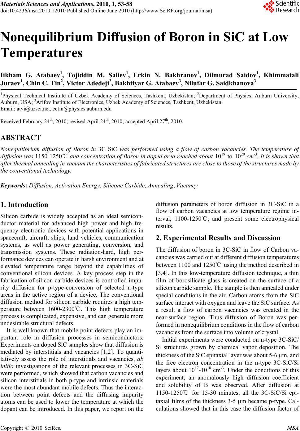 Materials Sciences and Applicatio ns, 2010, 1, 53-58 doi:10.4236/msa.2010.12010 Published Online June 2010 (http://www.SciRP.org/journal/msa) Copyright © 2010 SciRes. MSA Nonequilibrium Diffusion of Boron in SiC at Low Temperatures Iikham G. Atabaev1, Tojiddin M. Saliev1, Erkin N. Bakhranov1, Dilmurad Saidov1, Khimmatali Juraev1, Chin C. Tin2, Victor Adedeji2, Bakhtiyar G. Atabaev3, Nilufar G. Saidkhanova3 1Physical Technical Institute of Uzbek Academy of Sciences, Tashkent, Uzbekistan; 2Department of Physics, Auburn University, Auburn, USA; 3Arifov Institute of Electronics, Uzbek Academy of Sciences, Tashkent, Uzbekistan. Email: atvi@uzsci.net, cctin@physics.auburn.edu Received February 24th, 2010; revised April 24th, 2010; accepted April 27th, 2010. ABSTRACT Nonequilibrium diffusion of Boron in 3C SiC was performed using a flow of carbon vacancies. The temperature of diffusion was 1150-1250℃ and concentration of Boron in doped area reached about 1019 to 1020 cm -3. It is shown that after thermal annealing in vac uum the characteri stics of fabricated str uctures are close to t hose of the structures made by the conventional technology. Keywords: Diffusion, Activa tion Energy, Silicone Carb ide, Annealing, Vacancy 1. Introduction Silicon carbide is widely accepted as an ideal semicon- ductor material for advanced high power and high fre- quency electronic devices with potential applications in spacecraft, aircraft, ships, land vehicles, communication systems, as well as power generating, conversion, and transmission systems. These radiation-hard, high per- formance devices can operate in harsh environment and at elevated temperature range beyond the capabilities of conventional silicon devices. A key process step in the fabrication of silicon carbide devices is controlled impu- rity diffusion for p-type-conversion of selected n-type areas in the active region of a device. The conventional diffusion method for silicon carbide requires a high tem- perature between 1600-2300℃. This high temperature process is complicated, expensive, and can generate more undesirable structural defects. It is well known that mobile point defects play an im- portant role in diffusion processes in semiconductors. Experiments on doped SiC samples show that diffusion is mediated by interstitials and vacancies [1,2]. To quanti- tatively assess the role of interstitials and vacancies, ab initio investigations of the relevant processes in 3C-SiC were performed, which showed that carbon vacancies and silicon interstitials in both p-type and intrinsic materials were the most abundant mobile defects. Thus the interac- tion between point defects and the diffusing impurity atoms can be used to lower the temperature at which the dopant can be introduced. In this paper, we report on the diffusion parameters of boron diffusion in 3C-SiC in a flow of carbon vacancies at low temperature regime in- terval, 1100-1250℃, and present some electrophysical results. 2. Experimental Results and Discussion The diffusion of boron in 3C-SiC in flow of Carbon va- cancies was carried out at different diffusion temperatures between 1100 and 1250℃ using the method described in [3,4]. In this low-temperature diffusion technique, a thin film of borosilicate glass is created on the surface of a silicon carbide sample. The sample is then annealed under special conditions in the air. Carbon atoms from the SiC surface interact with oxygen and leave the SiC surface. As a result a flow of carbon vacancies was created in the near-surface region. Thus diffusion of Boron was per- formed in nonequilibrium conditions in the flow of carbon vacancies from the surface into volume of crystal. Initial experiments were conducted on n-type 3C-SiC/ Si structures grown by chemical vapor deposition. The thickness of the SiC epitaxial layer was about 5-6 m, and the free electron concentration in the n-type 3C-SiC/Si layers about 1017-1018 cm-3. Under the conditions of this experiment, an anomalously high diffusion coefficient and solubility of B was observed. After diffusion at 1150-1250℃ for 15-30 minutes, all the 3C-SiC/Si epi- taxial films of the thickness 3-5 m became р-type. Cal- culations showed that in this case the diffusion factor of 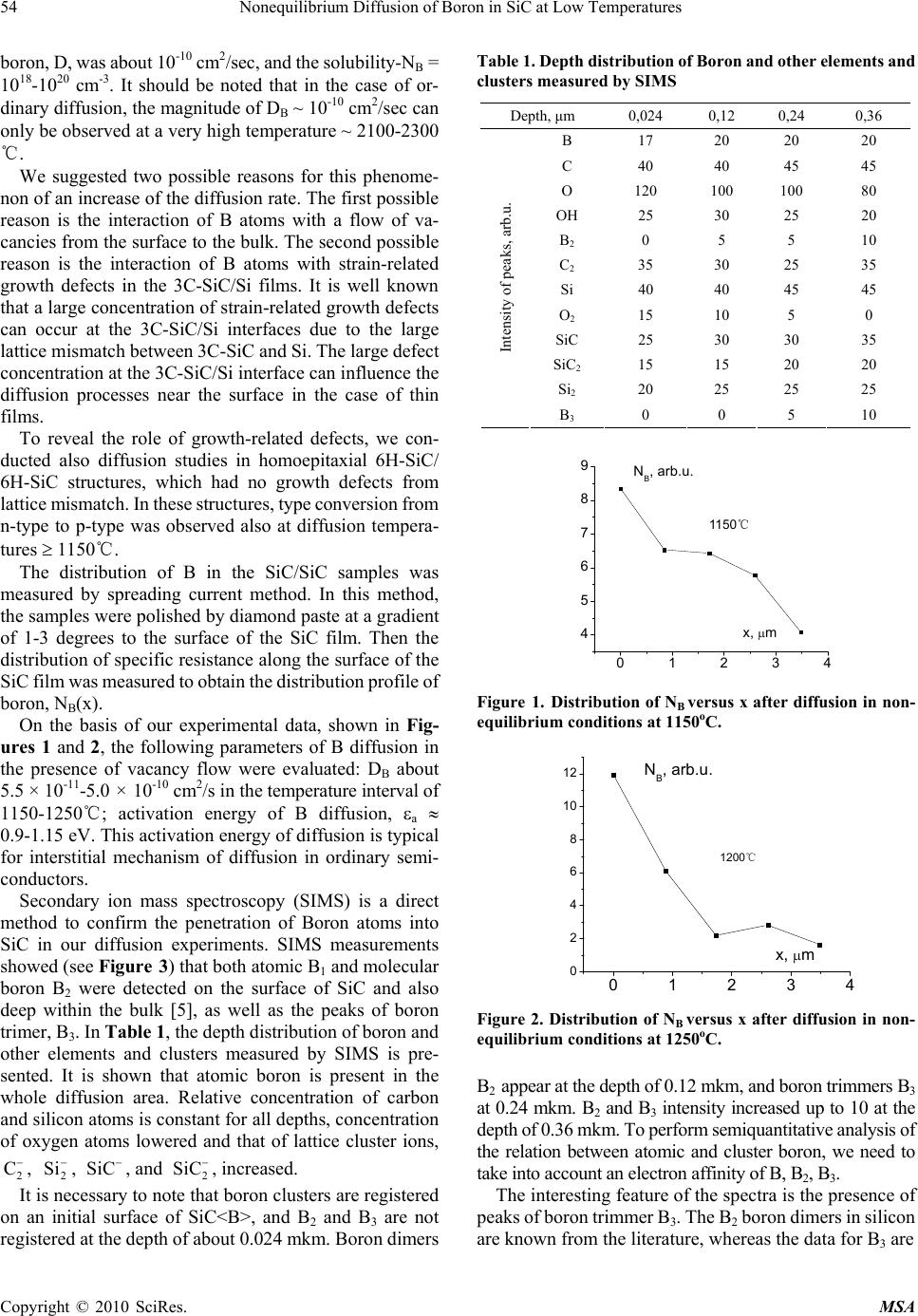 54 Nonequilibrium Diffusion of Boron in SiC at Low Temperatures boron, D, was about 10-10 cm2/sec, and the solubility-NB = 1018-1020 сm-3. It should be noted that in the case of or- dinary diffusion, the magnitude of DB ~ 10-10 cm2/sec can only be observed at a very high temperature ~ 2100-2300 ℃. We suggested two possible reasons for this phenome- non of an increase of the diffusion rate. The first possible reason is the interaction of B atoms with a flow of va- cancies from the surface to the bulk. The second possible reason is the interaction of B atoms with strain-related growth defects in the 3C-SiC/Si films. It is well known that a large concentration of strain-related growth defects can occur at the 3C-SiC/Si interfaces due to the large lattice mismatch between 3C-SiC and Si. The large defect concentration at the 3C-SiC/Si interface can influence the diffusion processes near the surface in the case of thin films. To reveal the role of growth-related defects, we con- ducted also diffusion studies in homoepitaxial 6H-SiC/ 6H-SiC structures, which had no growth defects from lattice mismatch. In these structures, type conversion from n-type to р-type was observed also at diffusion tempera- tures 1150℃. The distribution of B in the SiC/SiC samples was measured by spreading current method. In this method, the samples were polished by diamond paste at a gradient of 1-3 degrees to the surface of the SiC film. Then the distribution of specific resistance along the surface of the SiC film was measured to obtain the distribution profile of boron, NB(x). On the basis of our experimental data, shown in Fig- ures 1 and 2, the following parameters of B diffusion in the presence of vacancy flow were evaluated: DB about 5.5 × 10⁻¹¹-5.0 × 10⁻¹⁰ cm2/s in the temperature interval of 1150-1250℃; activation energy of B diffusion, a 0.9-1.15 eV. This activation energy of diffusion is typical for interstitial mechanism of diffusion in ordinary semi- conductors. Secondary ion mass spectroscopy (SIMS) is a direct method to confirm the penetration of Boron atoms into SiC in our diffusion experiments. SIMS measurements showed (see Figure 3) that both atomic B1 and molecular boron B2 were detected on the surface of SiC and also deep within the bulk [5], as well as the peaks of boron trimer, B3. In Table 1, the depth distribution of boron and other elements and clusters measured by SIMS is pre- sented. It is shown that atomic boron is present in the whole diffusion area. Relative concentration of carbon and silicon atoms is constant for all depths, concentration of oxygen atoms lowered and that of lattice cluster ions, , , , and , increased. 2 C 2 SiSiC 2 SiC It is necessary to note that boron clusters are registered on an initial surface of SiC<B>, and B2 and B3 are not registered at the depth of about 0.024 mkm. Boron dimers Table 1. Depth distribution of Boron and other elements and clusters measured by SIMS Depth, μm 0,024 0,12 0,24 0,36 В 17 20 20 20 C 40 40 45 45 O 120 100 100 80 OH 25 30 25 20 B2 0 5 5 10 C2 35 30 25 35 Si 40 40 45 45 O2 15 10 5 0 SiC 25 30 30 35 SiC2 15 15 20 20 Si2 20 25 25 25 Intensity of peaks, arb.u. B3 0 0 5 10 01234 4 5 6 7 8 9 1150 C x, m NB, arb.u. 115 0℃ Figure 1. Distribution of NB versus x after diffusion in non- equilibrium conditions at 1150оС. 01234 0 2 4 6 8 10 12 1200 C NB, arb.u. x, m 1200℃ Figure 2. Distribution of NB versus x after diffusion in non- equilibrium conditions at 1250оС. B2 appear at the depth of 0.12 mkm, and boron trimmers B3 at 0.24 mkm. B2 and B3 intensity increased up to 10 at the depth of 0.36 mkm. To perform semiquantitative analysis of the relation between atomic and cluster boron, we need to take into account an electron affinity of B, B2, B3. The interesting feature of the spectra is the presence of peaks of boron trimmer B3. The B2 boron dimers in silicon are known from the literature, whereas the data for B3 are Copyright © 2010 SciRes. MSA 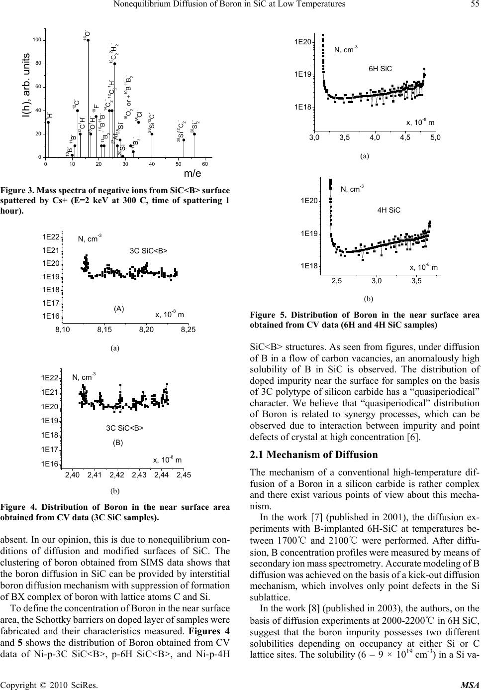 Nonequilibrium Diffusion of Boron in SiC at Low Temperatures 55 0 10203040506 0 20 40 60 80 100 0 16O2 - or +10B11B2 - 10B11B- I(h), arb. units m/e 28Si2 - 28Si12C2 - 28Si12C- 35Cl- 11B3 - 29Si-28Si- 27Al-12C2 2H2 - 12C2 1H- 16O1H-16O- 12C1H- 12C- 10B-11B- 1H- 14C2 - 11B2 - 19F- Figure 3. Mass spectra of negative ions from SiC<B> surface spattered by Cs+ (E=2 keV at 300 C, time of spattering 1 hour). 8,10 8,15 8,20 8,25 1E16 1E17 1E18 1E19 1E20 1E21 1E22 (A) x, 10-8 m N, cm-3 3C SiC<B> (a) 2,40 2,41 2,42 2,43 2,44 2,45 1E16 1E17 1E18 1E19 1E20 1E21 1E22 (B) 3C SiC<B> N, cm-3 x, 10-8 m (b) Figure 4. Distribution of Boron in the near surface area obtained from CV data (3C SiC samples). absent. In our opinion, this is due to nonequilibrium con- ditions of diffusion and modified surfaces of SiC. The clustering of boron obtained from SIMS data shows that the boron diffusion in SiC can be provided by interstitial boron diffusion mechanism with suppression of formation of BX complex of boron with lattice atoms C and Si. To define the concentration of Boron in the near surface area, the Schottky barriers on doped layer of samples were fabricated and their characteristics measured. Figures 4 and 5 shows the distribution of Boron obtained from CV data of Ni-p-3C SiC<B>, p-6Н SiC<B>, and Ni-p-4Н 3,0 3,5 4,0 4,5 5,0 1E18 1E19 1E20 N, cm-3 x, 10-8 m 6H SiC (a) 2,5 3,0 3,5 1E18 1E19 1E20 N, cm-3 x, 10-8 m 4H SiC (b) Figure 5. Distribution of Boron in the near surface area obtained from CV data (6H and 4H SiC samples) SiC<B> structures. As seen from figures, under diffusion of B in a flow of carbon vacancies, an anomalously high solubility of B in SiC is observed. The distribution of doped impurity near the surface for samples on the basis of 3C polytype of silicon carbide has a “quasiperiodical” character. We believe that “quasiperiodical” distribution of Boron is related to synergy processes, which can be observed due to interaction between impurity and point defects of crystal at high concentration [6]. 2.1 Mechanism of Diffusion The mechanism of a conventional high-temperature dif- fusion of a Boron in a silicon carbide is rather complex and there exist various points of view about this mecha- nism. In the work [7] (published in 2001), the diffusion ex- periments with B-implanted 6H-SiC at temperatures be- tween 1700℃ and 2100℃ were performed. After diffu- sion, B concentration profiles were measured by means of secondary ion mass spectrometry. Accurate modeling of B diffusion was achieved on the basis of a kick-out diffusion mechanism, which involves only point defects in the Si sublattice. In the work [8] (published in 2003), the authors, on the basis of diffusion experiments at 2000-2200℃ in 6H SiC, suggest that the boron impurity possesses two different solubilities depending on occupancy at either Si or C lattice sites. The solubility (6 – 9 × 1019 cm-3) in a Si va- Copyright © 2010 SciRes. MSA 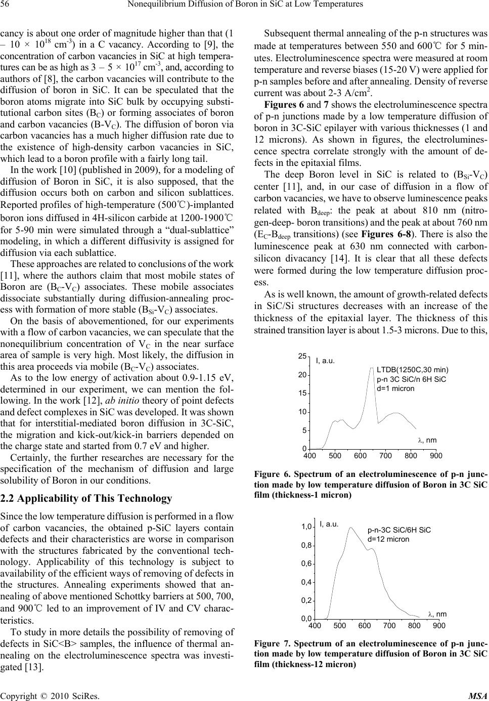 56 Nonequilibrium Diffusion of Boron in SiC at Low Temperatures cancy is about one order of magnitude higher than that (1 – 10 × 1018 cm-3) in a C vacancy. According to [9], the concentration of carbon vacancies in SiC at high tempera- tures can be as high as 3 – 5 × 1017 cm-3, and, according to authors of [8], the carbon vacancies will contribute to the diffusion of boron in SiC. It can be speculated that the boron atoms migrate into SiC bulk by occupying substi- tutional carbon sites (BC) or forming associates of boron and carbon vacancies (B-VC). The diffusion of boron via carbon vacancies has a much higher diffusion rate due to the existence of high-density carbon vacancies in SiC, which lead to a boron profile with a fairly long tail. In the work [10] (published in 2009), for a modeling of diffusion of Boron in SiC, it is also supposed, that the diffusion occurs both on carbon and silicon sublattices. Reported profiles of high-temperature (500℃)-implanted boron ions diffused in 4H-silicon carbide at 1200-1900℃ for 5-90 min were simulated through a “dual-sublattice” modeling, in which a different diffusivity is assigned for diffusion via each sublattice. These approaches are related to conclusions of the work [11], where the authors claim that most mobile states of Boron are (ВC-VC) associates. These mobile associates dissociate substantially during diffusion-annealing proc- ess with formation of more stable (BSi-VC) associates. On the basis of abovementioned, for our experiments with a flow of carbon vacancies, we can speculate that the nonequilibrium concentration of VC in the near surface area of sample is very high. Most likely, the diffusion in this area proceeds via mobile (ВC-VC) associates. As to the low energy of activation about 0.9-1.15 eV, determined in our experiment, we can mention the fol- lowing. In the work [12], ab initio theory of point defects and defect complexes in SiC was developed. It was shown that for interstitial-mediated boron diffusion in 3C-SiC, the migration and kick-out/kick-in barriers depended on the charge state and started from 0.7 eV and higher. Certainly, the further researches are necessary for the specification of the mechanism of diffusion and large solubility of Boron in our conditions. 2.2 Applicability of This Technology Since the low temperature diffusion is performed in a flow of carbon vacancies, the obtained p-SiC layers contain defects and their characteristics are worse in comparison with the structures fabricated by the conventional tech- nology. Applicability of this technology is subject to availability of the efficient ways of removing of defects in the structures. Annealing experiments showed that an- nealing of above mentioned Schottky barriers at 500, 700, and 900℃ led to an improvement of IV and CV charac- teristics. To study in more details the possibility of removing of defects in SiC<B> samples, the influence of thermal an- nealing on the electroluminescence spectra was investi- gated [13]. Subsequent thermal annealing of the p-n structures was made at temperatures between 550 and 600℃ for 5 min- utes. Electroluminescence spectra were measured at room temperature and reverse biases (15-20 V) were applied for p-n samples before and after annealing. Density of reverse current was about 2-3 A/cm2. Figures 6 and 7 shows the electroluminescence spectra of p-n junctions made by a low temperature diffusion of boron in 3C-SiC epilayer with various thicknesses (1 and 12 microns). As shown in figures, the electrolumines- cence spectra correlate strongly with the amount of de- fects in the epitaxial films. The deep Boron level in SiC is related to (BSi-VC) center [11], and, in our case of diffusion in a flow of carbon vacancies, we have to observe luminescence peaks related with Bdeep: the peak at about 810 nm (nitro- gen-deep- boron transitions) and the peak at about 760 nm (EC-Bdeep transitions) (see Figures 6-8). There is also the luminescence peak at 630 nm connected with carbon- silicon divacancy [14]. It is clear that all these defects were formed during the low temperature diffusion proc- ess. As is well known, the amount of growth-related defects in SiC/Si structures decreases with an increase of the thickness of the epitaxial layer. The thickness of this strained transition layer is about 1.5-3 microns. Due to this, 400 500 600 700 800 900 0 5 10 15 20 25 I, a.u. , nm LTDB(1250C,30 min) p-n 3C SiC/n 6H SiC d=1 micron Figure 6. Spectrum of an electroluminescence of p-n junc- tion made by low temperature diffusion of Boron in 3C SiC film (thickness-1 micron) 400 500 600 700 800 900 0,0 0,2 0,4 0,6 0,8 1,0 p-n-3C SiC/6H SiC d=12 micron , nm I, a.u. Figure 7. Spectrum of an electroluminescence of p-n junc- tion made by low temperature diffusion of Boron in 3C SiC film (thickness-12 micron) Copyright © 2010 SciRes. MSA 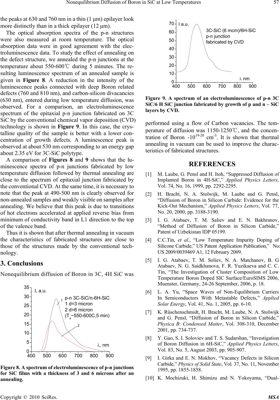 Nonequilibrium Diffusion of Boron in SiC at Low Temperatures 57 the peaks at 630 and 760 nm in a thin (1 μm) epilayer look more distinctly than in a thick epilayer (12 μm). The optical absorption spectra of the p-n structures were also measured at room temperature. The optical absorption data were in good agreement with the elec- troluminescence data. To study the effect of annealing on the defect structure, we annealed the p-n junctions at the temperature about 550-600℃ during 5 minutes. The re- sulting luminescence spectrum of an annealed sample is given in Figure 8. A reduction in the intensity of the luminescence peaks connected with deep Boron related defects (760 and 810 nm), and carbon-silicon divacancies (630 nm), entered during low temperature diffusion, was observed. For a comparison, an electroluminescence spectrum of the epitaxial p-n junction fabricated on 3C SiC by the conventional chemical vapor deposition (CVD) technology is shown in Figure 9. In this case, the crys- talline quality of the sample is better with a lower con- centration of growth defects. A luminescence peak is observed at about 530 nm corresponding to an energy gap about 2.35 eV for 3C-SiC polytype. A comparison of Figures 8 and 9 shows that the lu- minescence spectra of p-n junctions fabricated by low temperature diffusion followed by thermal annealing are close to the spectrum of epitaxial junction fabricated by the conventional CVD. At the same time, it is necessary to note that the peak at 490-500 nm is clearly observed for non-annealed samples and weakly visible on samples after annealing. We believe that this peak is due to transitions of hot electrons accelerated at applied reverse bias from minimum of conductivity band in L1 direction to the top of the valence band. Thus it is shown that after thermal annealing in vacuum the characteristics of fabricated structures are close to those of the structures made by the conventional tech- nology. 3. Conclusions Nonequilibrium diffusion of Boron in 3C, 4H SiC was 400 500 600 700 800 900 0 5 10 15 20 25 30 35 2 1 , nm I, a.u. p-n 3C-SiC/n-6H-SiC 1 d=3 micron 2 d=6 micron (T a ~550-600C,5 min) Figure 8. A spectrum of electroluminescence of p-n junctions for SiC films with a thickness of 3 and 6 microns after an annealing. 400 500 600 700 800 900 0 10 20 30 40 50 60 70 I a.u. nm 3C-SiC (6 mcm)/6H-SiC p-n junction fabricated by CVD Figure 9. A spectrum of an electroluminescence of p-n 3C SiC/6 H SiC junction fabricated by growth of p and n – SiC layers by CVD. performed using a flow of Carbon vacancies. The tem- perature of diffusion was 1150-1250℃, and the concen- tration of Boron -1019-20 cm-3. It is shown that thermal annealing in vacuum can be used to improve the charac- teristics of fabricated structures. REFERENCES [1] M. Laube, G. Pensl and H. Itoh, “Suppressed Diffusion of Implanted Boron in 4H-SiC,” Applied Physics Letters, Vol. 74, No. 16, 1999, pp. 2292-2295. [2] H. Bracht, N. A. Stolwijk, M. Laube and G. Pensl, “Diffusion of Boron in Silicon Carbide: Evidence for the Kick-Out Mechanism,” Applied Physics Letters, Vol. 77, No. 20, 2000, pp. 3188-3190. [3] I. G. Atabaev, T. M. Saliev and E. N. Bakhranov, “Method of Diffusion of Boron in Silicon Carbide,” Patent of Uzbekistan IDP 05199. [4] C.C.Tin, et al., “Low Temperature Impurity Doping of Silicone Carbide,” US Patent Application Publication,” No: US 2009/0039469 A1, 12 February 2009. [5] I. G. Atabaev, T. M. Soliev, N. A. Matchanov, B. G Atabaev, N. G. Saidkhanova, F. R. Yuzikaeva and C. C. Tin, “The Investigation of Cluster Composition of Low Temperature Boron Doped SIC Surface/EuroSIMS 2006, Muenster, Germany, 24-26 September, 2006, p. 18. [6] L. A. Yu, “Space Waves of Non-Equilibrium Carriers In Semiconductors With Metastable Defects,” Applied Solar Energy, Vol. 41, No. 1, 2005, pp. 6-10. [7] K. Rüschenschmidt, H. Bracht, M. Laube, N. A. Stolwijk and G. Pensl, “Diffusion of Boron in Silicon Carbide,” Physica B: Condensed Matter, Vol. 308-310, December 2001, pp. 734-737. [8] Y. Gao, S. I. Soloviev and T. S. Sudarshan, “Investigation of Boron Diffusion in 6H-SiC,” Applied Physics Letters, Vol. 83, No. 5, August 2003, pp. 905-907. [9] I. Girka and E. N. Mokhov, “Vacancy Defects in Silicon Carbide,” Physics of Solid State, Vol. 37, No. 11, November 1995, pp. 1855-1858. [10] K. Mochizuki, H. Shimizu and N. Yokoyama, “Dual- Copyright © 2010 SciRes. MSA 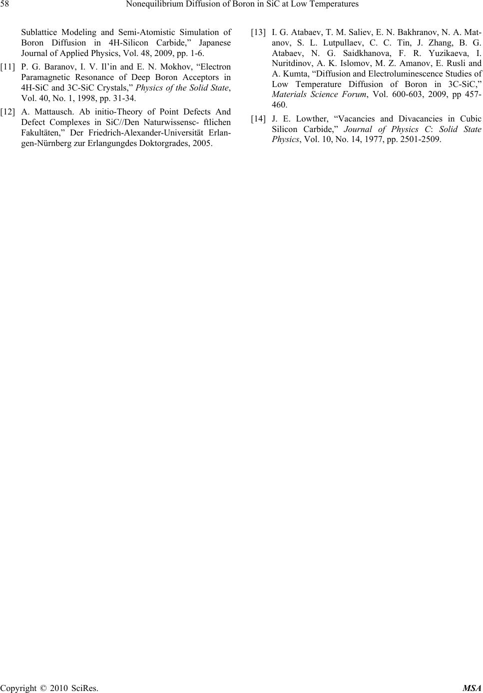 58 Nonequilibrium Diffusion of Boron in SiC at Low Temperatures Copyright © 2010 SciRes. MSA Sublattice Modeling and Semi-Atomistic Simulation of Boron Diffusion in 4H-Silicon Carbide,” Japanese Journal of Applied Physics, Vol. 48, 2009, pp. 1-6. [11] P. G. Baranov, I. V. Il’in and E. N. Mokhov, “Electron Paramagnetic Resonance of Deep Boron Acceptors in 4H-SiC and 3C-SiC Crystals,” Physics of the Solid State, Vol. 40, No. 1, 1998, pp. 31-34. [12] A. Mattausch. Ab initio-Theory of Point Defects And Defect Complexes in SiC//Den Naturwissensc- ftlichen Fakultäten,” Der Friedrich-Alexander-Universität Erlan- gen-Nürnberg zur Erlangungdes Doktorgrades, 2005. [13] I. G. Atabaev, T. M. Saliev, E. N. Bakhranov, N. A. Mat- anov, S. L. Lutpullaev, C. C. Tin, J. Zhang, B. G. Atabaev, N. G. Saidkhanova, F. R. Yuzikaeva, I. Nuritdinov, A. K. Islomov, M. Z. Amanov, E. Rusli and A. Kumta, “Diffusion and Electroluminescence Studies of Low Temperature Diffusion of Boron in 3C-SiC,” Materials Science Forum, Vol. 600-603, 2009, pp 457- 460. [14] J. E. Lowther, “Vacancies and Divacancies in Cubic Silicon Carbide,” Journal of Physics C: Solid State Physics, Vol. 10, No. 14, 1977, pp. 2501-2509. |