Paper Menu >>
Journal Menu >>
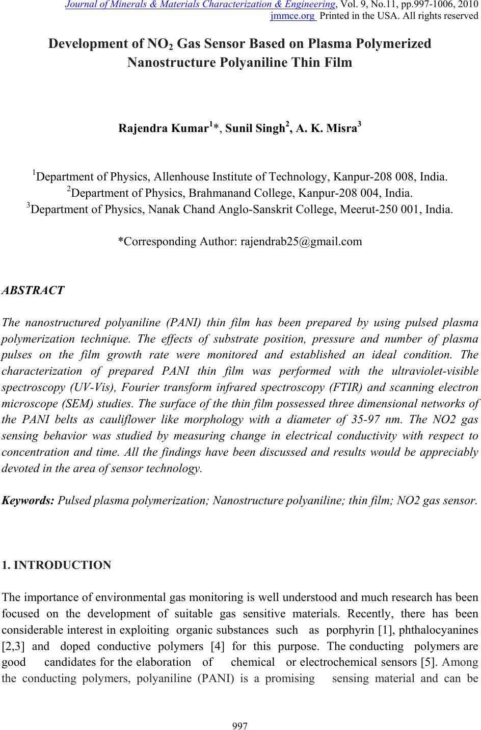 Journal of Minerals & Materials Characterization & Engineering, Vol. 9, No.11, pp.997-1006, 2010 jmmce.org Printed in the USA. All rights reserved 997 Development of NO2 Gas Sensor Based on Plasma Polymerized Nanostructure Polyaniline Thin Film Rajendra Kumar1*, Sunil Singh2, A. K. Misra3 1Department of Physics, Allenhouse Institute of Technology, Kanpur-208 008, India. 2Department of Physics, Brahmanand College, Kanpur-208 004, India. 3Department of Physics, Nanak Chand Anglo-Sanskrit College, Meerut-250 001, India. *Corresponding Author: rajendrab25@gmail.com ABSTRACT The nanostructured polyaniline (PANI) thin film has been prepared by using pulsed plasma polymerization technique. The effects of substrate position, pressure and number of plasma pulses on the film growth rate were monitored and established an ideal condition. The characterization of prepared PANI thin film was performed with the ultraviolet-visible spectroscopy (UV-Vis), Fourier transform infrared spectroscopy (FTIR) and scanning electron microscope (SEM) studies. The surface of the thin film possessed three dimensional networks of the PANI belts as cauliflower like morphology with a diameter of 35-97 nm. The NO2 gas sensing behavior was studied by measuring change in electrical conductivity with respect to concentration and time. All the findings have been discussed and results would be appreciably devoted in the area of sensor technology. Keywords: Pulsed plasma polymerization; Nanostructure polyaniline; thin film; NO2 gas sensor. 1. INTRODUCTION The importance of environmental gas monitoring is well understood and much research has been focused on the development of suitable gas sensitive materials. Recently, there has been considerable interest in exploiting organic substances such as porphyrin [1], phthalocyanines [2,3] and doped conductive polymers [4] for this purpose. The conducting polymers are good candidates for the elaboration of chemical or electrochemical sensors [5]. Among the conducting polymers, polyaniline (PANI) is a promising sensing material and can be  998 Rajendra Kumar, Sunil Singh, A. K. Misra Vol.9, No.11 synthesized by chemical, electrochemical, or plasma methods, and in each case, the composition, morphology, and physical properties of the resulting polymer are strongly dependent on the detailed reaction conditions [6]. Plasma polymerization technique is unique because of denseness, uniform film thickness, adhesion conformability on substrates and has less chemical processability, etc. [7]. It has been used to prepare films of a wide range of the conducting polymers including PANI [8, 9]. The composition of a plasma-polymerized film can be tailored with the appropriate processing conditions, and the properties of resulting material are often unique and unobtainable by wet synthetic methods [10]. Although the excited plasma species are mainly high-energy electrons that are relatively indiscriminate in rupturing chemical bonds, the substrate can be kept at the ambient temperature [11]. The observation of the semi-conducting properties of PANI thin films are modulated by the absorption and de-sorption of gases has led to significant efforts toward their incorporation in chemical/gas sensors [12]. The nanostructured PANI has attracted the attention because of its increase selective, sensitivity and quick response [13]. Medema et al has reported PANI thin film based sensor [14] and observed excellent change in the conductivity with the exposure of the analyte onto the sublimed PANI film. In the present communication, we report an ideal pulse-plasma polymerization condition for the preparation of nanostructured PANI thin film and its application for the detection of NO2 gas. 2. EXPERIMENTAL 2.1 Instrumentation A handmade-assembled plasma reactor was used for the preparation of PANI thin film. In the system, thermocouples gauge (GIC-11-B, Veeco Instruments Inc.) and capacitance manometer (627A01TBC, MKS Baratron) was attached for the monitoring of the reactor pressure. The calibration of manometer was performed in triplicate from 0 to 1000 mTorr with the air, aniline vapor, and a mixture of aniline vapor and hydrogen. Once enough monomer was injected into the plasma reactor at the desired deposition pressure, the plasma was repetitively activated through the discharge of a 1.8-μF capacitor initially held at 23 kV, the RF coil excitation being with a damped sinusoid of 290 kHz and a decay time constant of 10 μs. After 10 plasma shots, the reactor was evacuated completely and refilled with fresh monomer vapor. One hundred plasma pulses were used to grow PANI samples. The substrate holder was movable and can be positioned at various distances from the RF coil. The glass substrate with inter digited gold, indium tin oxide (ITO) coated glass and glass slides was used as substrate to deposit the PANI. The reagent-grade aniline (Aldrich; 99.5%) monomer was purified by triple distillation over zinc granules and stored in a dark bottle under nitrogen. The thickness of representative plasma- polymerized PANI films was measure by using profilometer (SPN Technology).  Vol.9, No.11 Development of NO2 Gas Sensor 999 2.2 Preparation of PANI Thin Film PANI thin films have been prepared by an inductively coupled pulsed-plasma reactor at different RF plasma pulsing, monomer injection, and substrate positions. The custom built automotive injector with an oscilloscope was used to control the injection of vaporized aniline monomer under pressure. Since a pulse of the aniline entered into the evacuated reactor, most of the liquid immediately vaporized by flash boiling and the remaining liquid disintegrated into droplets that were collected by mesh separators placed about 2 cm from the injector nozzle. The aniline was injected with 10 ms pulses at 40 Pa reactor’s pressure into the plasma reactor. All the depositions were performed with a static fill of aniline vapor and the electrical pulses that polymerized to form PANI thin film over the substrate surface. 2.3 Characterization PANI thin film was characterized with the UV-Vis, FTIR and SEM measurements. An Ocean optics HR 4000 high resolution spectrophotometer was used to record the UV-Vis spectra. FTIR recorded with a PerkinElmer BX FTIR using pressed KBr pellet, while scanning electron microscopy (SEM) was studied on the using a LEO-440 with the gold sputtered PANI thin film. 2.4 Fabrication of Sensing Electrode On the clean inter digited gold glass substrate; the 2 leads (copper wires) were attached by silver paste then PANI thin film was deposited on the open area between the two electrodes with the pulsed plasma technique as described. The electrical conductivity of the sensor was monitored, by continuously recording currents at constant potential using a stabilized DC power supply, a Keithley electrometer and a fast x-y-t recorder [Lienses, Germany]. Fig. 1 gives details of such a PANI thin film to be used as sensor. Fig. 1. Schematic diagram of inter digited PANI thin film prepared via plasma polymerization technique based NO2 sensing probe.  1000 Rajendra Kumar, Sunil Singh, A. K. Misra Vol.9, No.11 2.5 Design and Construction of NO2 Gas Sensor There was an arrangement as shown in Fig. 2 to allow NO2 gas sensing with PANI thin film probe (Fig. 1). The sensor could be kept in a chamber. The NO2 gas was dilute with the purified air as mixed in the certain ppm range that passed in a chamber, inside which an inter digited PANI thin film electrode was kept. The unused NO2 mixture could be taken out of the chamber as exhaust gas. The current through the film could be measured and this could be read directly and converted into DC resistance value (R) of the PANI sensor electrode. Fig. 2. A schematic diagram showing the gas sensing measurement. 3. RESULTS AND DISCUSSION 3.1 Film Deposition Rate The variation in the film thickness was observed with the net growth rate of the PANI film over the substrate under different conditions. As Table-1 indicates, the profilometer data are directly 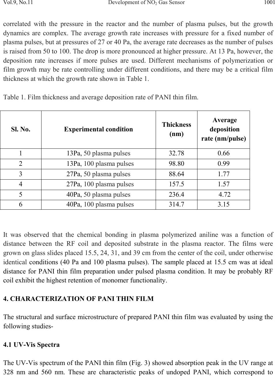 Vol.9, No.11 Development of NO2 Gas Sensor 1001 correlated with the pressure in the reactor and the number of plasma pulses, but the growth dynamics are complex. The average growth rate increases with pressure for a fixed number of plasma pulses, but at pressures of 27 or 40 Pa, the average rate decreases as the number of pulses is raised from 50 to 100. The drop is more pronounced at higher pressure. At 13 Pa, however, the deposition rate increases if more pulses are used. Different mechanisms of polymerization or film growth may be rate controlling under different conditions, and there may be a critical film thickness at which the growth rate shown in Table 1. Table 1. Film thickness and average deposition rate of PANI thin film. It was observed that the chemical bonding in plasma polymerized aniline was a function of distance between the RF coil and deposited substrate in the plasma reactor. The films were grown on glass slides placed 15.5, 24, 31, and 39 cm from the center of the coil, under otherwise identical conditions (40 Pa and 100 plasma pulses). The sample placed at 15.5 cm was at ideal distance for PANI thin film preparation under pulsed plasma condition. It may be probably RF coil exhibit the highest retention of monomer functionality. 4. CHARACTERIZATION OF PANI THIN FILM The structural and surface microstructure of prepared PANI thin film was evaluated by using the following studies- 4.1 UV-Vis Spectra The UV-Vis spectrum of the PANI thin film (Fig. 3) showed absorption peak in the UV range at 328 nm and 560 nm. These are characteristic peaks of undoped PANI, which correspond to Sl. No. Experimental conditi on Thickness (nm) Average deposition rate (nm/pulse) 1 13Pa, 50 plasma pulses 32.78 0.66 2 13Pa, 100 plasma pulses 98.80 0.99 3 27Pa, 50 plasma pulses 88.64 1.77 4 27Pa, 100 plasma pulses 157.5 1.57 5 40Pa, 50 plasma pulses 236.4 4.72 6 40Pa, 100 plasma pulses 314.7 3.15 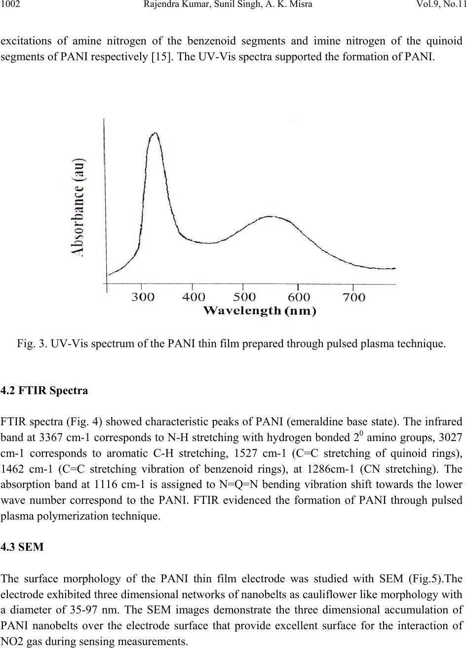 1002 Rajendra Kumar, Sunil Singh, A. K. Misra Vol.9, No.11 excitations of amine nitrogen of the benzenoid segments and imine nitrogen of the quinoid segments of PANI respectively [15]. The UV-Vis spectra supported the formation of PANI. Fig. 3. UV-Vis spectrum of the PANI thin film prepared through pulsed plasma technique. 4.2 FTIR Spectra FTIR spectra (Fig. 4) showed characteristic peaks of PANI (emeraldine base state). The infrared band at 3367 cm-1 corresponds to N-H stretching with hydrogen bonded 20 amino groups, 3027 cm-1 corresponds to aromatic C-H stretching, 1527 cm-1 (C=C stretching of quinoid rings), 1462 cm-1 (C=C stretching vibration of benzenoid rings), at 1286cm-1 (CN stretching). The absorption band at 1116 cm-1 is assigned to N=Q=N bending vibration shift towards the lower wave number correspond to the PANI. FTIR evidenced the formation of PANI through pulsed plasma polymerization technique. 4.3 SEM The surface morphology of the PANI thin film electrode was studied with SEM (Fig.5).The electrode exhibited three dimensional networks of nanobelts as cauliflower like morphology with a diameter of 35-97 nm. The SEM images demonstrate the three dimensional accumulation of PANI nanobelts over the electrode surface that provide excellent surface for the interaction of NO2 gas during sensing measurements. 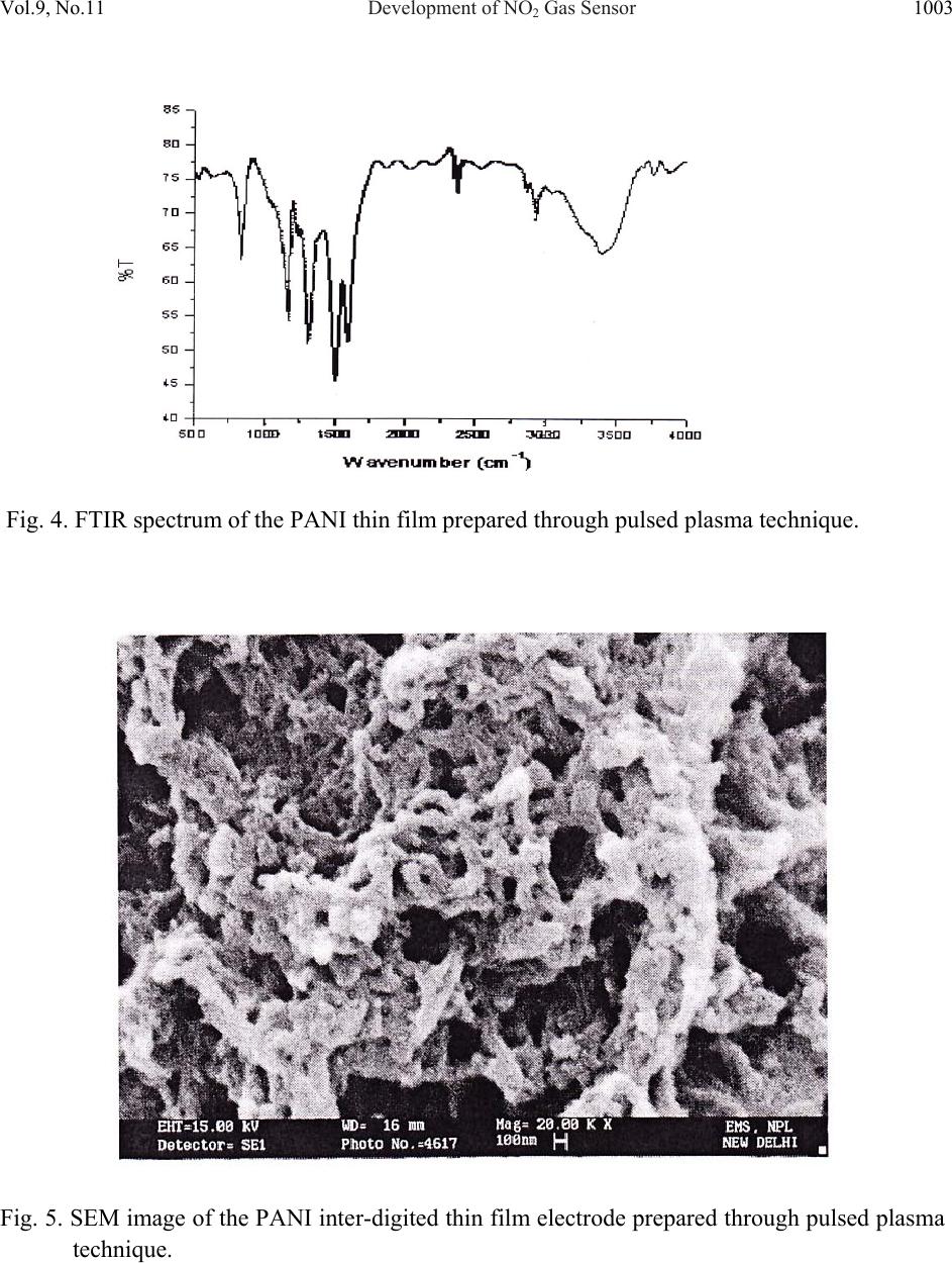 Vol.9, No.11 Development of NO2 Gas Sensor 1003 Fig. 4. FTIR spectrum of the PANI thin film prepared through pulsed plasma technique. Fig. 5. SEM image of the PANI inter-digited thin film electrode prepared through pulsed plasma technique. 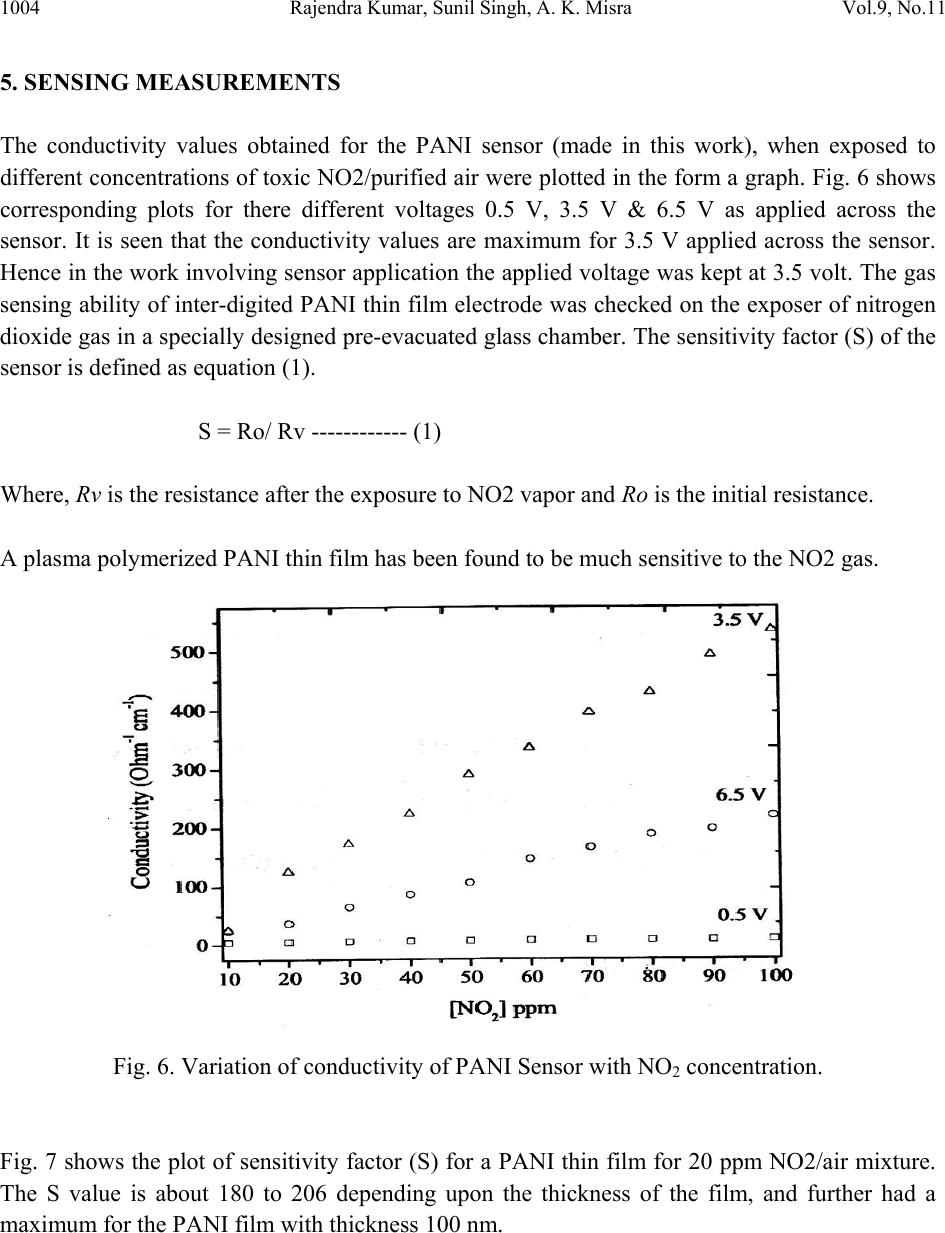 1004 Rajendra Kumar, Sunil Singh, A. K. Misra Vol.9, No.11 5. SENSING MEASUREMENTS The conductivity values obtained for the PANI sensor (made in this work), when exposed to different concentrations of toxic NO2/purified air were plotted in the form a graph. Fig. 6 shows corresponding plots for there different voltages 0.5 V, 3.5 V & 6.5 V as applied across the sensor. It is seen that the conductivity values are maximum for 3.5 V applied across the sensor. Hence in the work involving sensor application the applied voltage was kept at 3.5 volt. The gas sensing ability of inter-digited PANI thin film electrode was checked on the exposer of nitrogen dioxide gas in a specially designed pre-evacuated glass chamber. The sensitivity factor (S) of the sensor is defined as equation (1). S = Ro/ Rv ------------ (1) Where, Rv is the resistance after the exposure to NO2 vapor and Ro is the initial resistance. A plasma polymerized PANI thin film has been found to be much sensitive to the NO2 gas. Fig. 6. Variation of conductivity of PANI Sensor with NO2 concentration. Fig. 7 shows the plot of sensitivity factor (S) for a PANI thin film for 20 ppm NO2/air mixture. The S value is about 180 to 206 depending upon the thickness of the film, and further had a maximum for the PANI film with thickness 100 nm. 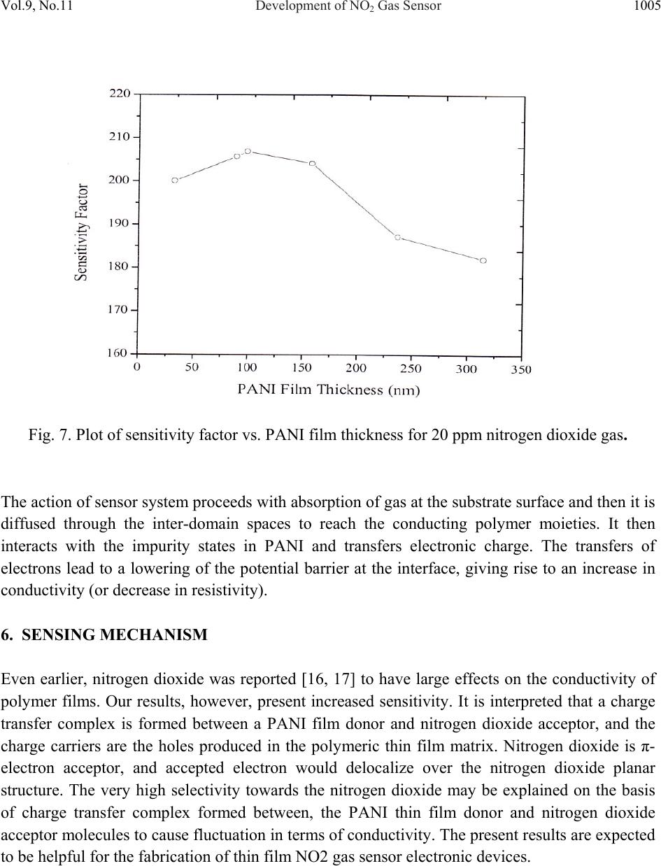 Vol.9, No.11 Development of NO2 Gas Sensor 1005 Fig. 7. Plot of sensitivity factor vs. PANI film thickness for 20 ppm nitrogen dioxide gas. The action of sensor system proceeds with absorption of gas at the substrate surface and then it is diffused through the inter-domain spaces to reach the conducting polymer moieties. It then interacts with the impurity states in PANI and transfers electronic charge. The transfers of electrons lead to a lowering of the potential barrier at the interface, giving rise to an increase in conductivity (or decrease in resistivity). 6. SENSING MECHANISM Even earlier, nitrogen dioxide was reported [16, 17] to have large effects on the conductivity of polymer films. Our results, however, present increased sensitivity. It is interpreted that a charge transfer complex is formed between a PANI film donor and nitrogen dioxide acceptor, and the charge carriers are the holes produced in the polymeric thin film matrix. Nitrogen dioxide is π- electron acceptor, and accepted electron would delocalize over the nitrogen dioxide planar structure. The very high selectivity towards the nitrogen dioxide may be explained on the basis of charge transfer complex formed between, the PANI thin film donor and nitrogen dioxide acceptor molecules to cause fluctuation in terms of conductivity. The present results are expected to be helpful for the fabrication of thin film NO2 gas sensor electronic devices.  1006 Rajendra Kumar, Sunil Singh, A. K. Misra Vol.9, No.11 7. CONCLUSIONS The nanostructured PANI thin films have been prepared under inductively coupled pulsed- plasma reactor. The ultra thin films of PANI were prepared by varying the conditions under the RF plasma operated in a pulsed manner. The RF frequency was directed and controlled the PANI cross-linking growth rate on the substrate. The prepared ultra thin film showed emeraldine base state of PANI and showed electronic change with the exposure of NO2 gas over the sensing electrode. REFERENCES [1] D. G. Zhu, D. F. Cui, M. Harris, M. C. Petty, Sensors & Actuators B, 1993, 12, 111-114. [2] J. D. Wright, P. Roisin, G. P. Rigby, R. J. M. Nolte, S. C. Thorpe, Sensors & Actuators B, 1994, 13, 276-280. [3] P. S. Vukusic, J. R. Shambles, Thin Solid Films, 1992, 221, 311-317. [4] P. N. Bartlett, S.K. Liang-Chung, Sensors & Actuators, 1989, 20,287-292. [5] J. J. Miasik, A. Hooper, B. C. Tofield, J. Chem. Soc. Faraday Trans-I, 1986, 82, 1117-1126. [6] N. K. Svelko, F. Dinant, S. Magana, G. Clisson, J. François, C. D. Lartigau, S. Reynaud, Polymer International, 2006, 55, 1184-1190. [7] L. M. Han, R. B. Timmons, J. Polym. Sci. Part A: Polym Chem, 1998, 36, 3121- 3129. [8] L. V. Shepsis, P. D. Pedrow, R. Mahalingam, M. A. Osman, Thin Solid Films, 2001, 385, 11-21. [9] M. Augestine, M. Sebastian, K. A. Malini, M. J. S. Joseph, T. Joseph, D. Sakthikumar, S. Jayalakshmi, T. M. S. Rasheed, M. R. Anantharaman, Indian J. Pure Appl. Phys, 1996, 34, 966-972. [10] C. J. Mathai, S. Saravanan, M. R. Anantharaman, S. Venkitachalam, S. Jayalekshmi, J. Phys D: Appl Phys, 2002, 35, 240-245. [11] R. K. Sadhir, K. F. J. Schoch, Thin Solid Films, 1993,223, 154-160. [12] H. Bai, G. Shi, Sensors, 2007, 7, 267-307. [13] X. Luo, G. D. Vidal, A. J. Killard, A. Morrin, M. R. Smyth, Electroanalysis, 2007, 19, 876- 883. [14] J. Medema, V. D. Leeuwen, V. G. Kirsch, J. Electroanal Chem.,1972, 37, 373-378. [15] A. Tiwari, Journal of Macromolecular Science Part A, 2007, 44, 735-745. [16] R. L. Ewyk, A. V. Chadwick, J. D. Wright, J. Chem. Soc. Faraday Trans-I, 1980, 76, 2194- 2205. [17] S. Radhakrishnan, S. G. Joshi, J. Polym. Sci., Part C: Polym. Lett, 1989, 27, 127-131. |