Paper Menu >>
Journal Menu >>
 Journal of Minerals & Materials Characterization & Engineering, Vol. 5, No.2, pp 143-153, 2006 jmmce.org Printed in the USA. All rights reserved 143 Structural and microstructural characteristics of B-doped PbTe semiconductor Jovica N. Stojanovic Institute for Technology of Nuclear and Other Raw Mineral Materials, Applied Mineralogy Unit, Franche d‘Eperey 86, P.O. Box 390, 11000 Belgrade, Serbia E-mail: j.stojanovic@itnms.ac.yu, Phone: +381-11-3691-722 Abstract: The main task of this paper was accurate determination of structural and microstructural parameters of B-doped PbTe semiconductor (“p” type). Four samples (undoped PbTe, and three doped with initial B contents: 1 %, 3 % and 8 %) were synthesized using the Bridgman method and analysed using X-ray powder diffraction (XRD) technique. Structural features were obtained using the Rietveld method and microstructural by diffraction-line broadening methods. Microstructural measurements contain both crystallite domain sizes and microstrain calculations obtained by the Warren-Averbach and the simplified integral-breadth methods. Keywords: B-doped PbTe semiconductor, the Rietveld method, microstructural measurements. INTRODUCTION PbTe is a narrow-gap semiconductor. The research in doping of semiconductor materials and hereby modified properties is one of the most significant tasks of modern semiconductor physics. Great consideration is given to optical, photoelectric and magnetic features of AIVBVI compounds doped with some elements from the III group (B, Al, Ga, In, Tl). The most studied compounds, thus far, are In, Ga and Tl- doped AIVBVI compounds. B-doped PbTe is one serial semiconductor material, important in manufacturing of laser and detector infrared (IR) optoelectronics within wavelength from 1 to 40 µm.  144 Stojanovic Vol.5, No.2 The scope of the paper is to give an answer with the reference to the issues of how and where B atoms have sited into PbTe structure. Rietveld refinement method was used for structural and crystallite domain-size as well as crystal lattice microstrain calculations for microstructural determinations. Both crystallite domain size and microstrain measurements were calculated towards obtaining the crystallographic direction distributions of B atoms. The Warren-Averbach method and corresponding microstrain calculations were applied in diffraction-line broadening measurements for surface-weighted (<D>S) and volume-weighted <D>V), crystallite domain sizes. The referred measurements were also done by applying “simplified” integral-breadth methods: 1) broadenings originated due to both crystallite domain sizes and microstrains, which correspond to the Cauchy function, 2) the Gauss function and 3) both broadenings originated due to crystallite domain sizes that correspond to the Cauchy function and microstrains that correspond to the Gauss function. The last one provides for an excellent theoretical basis and it is widely applied in various Rietveld analysis softwares intended to microstructural calculations. EXPERIMENT AND ANALY TICAL METHODS B-doped PbTe samples were synthesized using the Bridgman method. Pb and Te were applied in an ingot form, of a normal 99.99 wt% purity. So derived samples were further powdered for XRD analyses. Four samples were synthesized in the Institute of Technical Sciences of the Serbian Academy of Sciences and Arts: undoped PbTe, PbTe doped with B (1 at.%, 3 at.% and 8 at.%). X-ray intensity measurements were carried out on a PHILIPS PW 1710 automated diffractometer. The powder diffraction data are given in Table 1. The FULLPROF software [2] was used for the Rietveld structure refinement and BREADTH [1] for the diffraction-line broadening measurements. RESULTS AND DISCUS SI ON Rietveld structure refinement PbTe is cubic, space group mFm3 with Z=4. Both Pb and Te atoms are in fixed positions at ½½½ and 000 respectively, and both atoms are in octahedral  Vol.5, No.2 Structural and Microstructural Characteristics 145 coordination. Table 1. Rietveld powder diffraction data for B-doped PbTe. Sample characterization Name (chemical, mineral) Lead telluride (altaite) Empirical formula PbTe Source/preparation synthetic Technique Radiation type, source X-rays, Cu λ value used 1.54060Å Kα1/1.54439 Kα2 Monochromator diffracted beam graphite monochromator Detector (film, scint. etc) Instrument description (type, slits) proportional vertical diffractometer divergence slit 1o receiving slit 0.1 mm soller slit 1o Instrumental profile breadth 0.10 o2θ temp. (oC) 25 ± 1 Specimen form/particle size Range of 2θ Specimen motion edge loaded powder/ <10 µm particle size from 20 o to 140 o2θ, 4 s per step none There were no other phases except PbTe during the treatments. Even the reflection displacements did not occur. Therefore, the conclusion is that B atoms haven’t deranged the PbTe structure when sited in it. (200) reflection showed strong, while (220) and (222) reflection showed appreciably weaker preferred orientation effects in all sample. The observed (circles), calculated (continuous line) and difference powder diffraction profiles for all analysed samples are shown in Figure 1. The Rietveld agreement factors are presented in Table 2. Table 2. Rietveld refinement agreement factors PbTe PbTe+B (1%) PbTe+B (3%) PbTe+B (8%) Rexp 11.4 10.7 11.3 10.5 Rp 13.3 12.7 14.2 12.4 Rwp 14.3 14.1 14.9 14.8 RB 6.12 5.58 5.69 5.82 RF 6.47 5.55 5.28 6.48 GofF 1.6 1.7 1.6 1.7 The unit-cell parameter of pure PbTe is in a good agreement with all B-doped 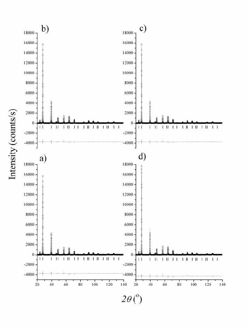 146 Stojanovic Vol.5, No.2 samples and literature data [4] as well. The isotropic displacement parameters of Figure 1. The observed (circles), calculated (continuous line) and difference powder diffraction profiles for: a) undoped PbTe, b) PbTe doped with B 1 at%, c) PbTe doped with B 3 at% and d) PbTe doped with B 8 at%.  Vol.5, No.2 Structural and Microstructural Characteristics 147 Pb atoms have been observed to be larger than those of Te atoms, which can indicate thermal vibration increment of the Pb sublattice to that of the Te sublattice, especially in samples doped with 1 and 8 %. However, this is not an unusual phenomenon. Even in pure PbTe crystals, the relatively large anharmonic thermal vibrations of Pb lattice to that of the Te sublattice along the [hhh] direction were observed [3]. According to the same data these thermal vibrations of Pb atoms are enhanced by the alloying elements Ge or Sn and make a lattice unstable. Unit-cell and isotropic displacement parameters in comparison to the literature data [4] are given in Table 3. Table 3. Rietveld refinement unit-cell and isotropic displacement parameters in comparison to the literature data. PbTe PbTe+B (1%) PbTe+B (3%) PbTe+B (8%) YASUTOSHI et al. (1987) Biso Pb (Å2) 2.037(2) 2.661(1) 2.109(7) 2.648(1) 1.61(2) Biso Te (Å2) 1.126(2) 1.319(2) 1.267(1) 1.426(6) 1.11(1) BisoPb/BisoTe 1.809 2.017 1.665 1.856 1.45 a (Å) 6.4603(2) 6.4605(2) 6.4601(7) 6.4605(2) 6.4541(9) V (Å3) 269.62(1) 269.65(2) 269.60(5) 269.65(1) 268.85 Microstructural measurements Microstructural parameter calculations were measured in crystallographic directions as follows: [h00]-(200), (400), (600); [hh0]-(220) (440); [hhh]-(111), (222), (333) (444); [hkk]-(311), (622) [h00] and [hh0] layers consist of both Pb and Te atoms while [hhh] and [hkk] layers consist of either Pb or Te atoms. So, the (311) layer consists entirely of Te atoms and the (622) one of Pb atoms. Likewise, (111) and (333) layers consist entirely of Te atoms; the (222) and (444) layers consist entirely of Pb atoms. Diffraction-line broadening measurements containing both crystallite domain sizes and microstrain parameters obtained by the Warren-Averbach and the simplified integral-breadth methods are given in Tables 4-7.  148 Stojanovic Vol.5, No.2 Table 4. Crystallite domain sizes obtained by the Warren-Averbach method. D (Å) h 0 0 h h 0 h h h h k k PbTe <D>s* 480 ± 36 357 ± 29 466 ± 64 163 ± 82 <D>v** 484 ± 14 443 ± 19 484± 27 315 ±113 PbTe+B(1%) <D>s 498 ± 43 428 ± 38 476 ± 46 312 ± 25 <D>v 543 ± 20 482 ± 20 546 ± 24 421 ± 20 PbTe+B(3%) <D>s 417 ± 46 339 ± 30 394 ± 63 235 ± 18 <D>v 406 ± 17 362 ± 14 407 ± 26 314 ± 14 PbTe+B(8%) <D>s 554 ± 38 430 ± 54 448 ± 51 330 ± 41 <D>v 583 ± 16 536 ± 36 545 ± 46 479 ± 38 * Surface-weighted domain size. ** Volume- weighted domain size. Table 5. Microstrain parameters obtained by the Warren-Averbach method. 2/1 2 ε (10-3) h 0 0 h h 0 h h h h k k 2/1 2/ 2 S D ε * 0.89 ± 0.03 0.99 ± 0.05 0.66 ± 0.05 0.72 ± 0.02 PbTe 2/1 2/ 2 V D ε ** 0.88 ± 0.02 0.89 ± 0.04 0.68 ± 0.05 0.75 ± 0.02 2/1 2/ 2 S D ε 0.95 ± 0.03 1.05 ± 0.03 0.77 ± 0.03 0.84 ±0.05 PbTe+B(1%) 2/1 2/ 2 V D ε 0.91 ± 0.02 0.94 ± 0.03 0.72 ± 0.03 0.73 ± 0.04 2/1 2/ 2 S D ε 1.18 ± 0.04 1.33 ± 0.04 0.91 ± 0.06 0.99 ± 0.07 PbTe+B(3%) 2/1 2/ 2 V D ε 1.19 ± 0.04 1.29 ± 0.04 0.89 ± 0.06 0.86 ± 0.06 2/1 2/ 2 S D ε 0.80 ± 0.02 0.89 ± 0.06 0.64 ± 0.01 0.68 ± 0.08 PbTe+B(8%) 2/1 2/ 2 V D ε 0.78 ± 0.02 0.80 ± 0.05 0.53 ± 0.01 0.56 ± 0.07 * Root-mean-square microstrain (RMSM) averaged over the distance <D>s. ** RMSM averaged over the distance <D>v.  Vol.5, No.2 Structural and Microstructural Characteristics 149 Table 6. Crystallite domain sizes obtained by the simplified integral-breadth methods. D (Å) h 0 0 h h 0 h h h h k k <DC-C>* 524 491 467 271 <DC-G>** 454 446 446 323 PbTe <DG-G> *** 451 443 443 319 <DC-C> 652 619 569 454 <DC-G> 523 509 463 421 PbTe+B(1%) <DG-G> 506 493 460 420 <DC-C> 469 441 403 317 <DC-G> 384 374 366 311 PbTe+B(3%) <DG-G> 375 368 361 311 <DC-C> 672 638 617 502 <DC-G> 562 551 539 479 PbTe +B(8%) <DG-G> 555 544 538 478 Volume-averaged domain size from the simplified integral-breadth methods: * Cauchy-Cauchy function, ** Cauchy-Gauss function, *** Gauss-Gauss function. Microstrain parameters of both the Warren-Averbach and the simplified integral- breadth methods increase up to the sample doped with 3 %, to be followed by a rapid decrease in the sample doped with 8% of B. This trend is noticeable along each measured crystallographic direction. The referred phenomenon can be explained by B atoms, sited in PbTe structure, in two different manners. Besides, microstrain parameters in the directions, consisting of layers with homogeneous atoms, are much lower in comparison to the parameters with heterogeneous atoms. Taking into consideration all these facts, the basic assumption is that high microstrain values appear as the result of vacancy arrangements in the directions where the layers consist of heterogeneous atoms (Pb and Te). The point to be emphasised is that the values of the kind were measured in all samples, meaning they are not resulting from B atoms disposition. If so, such values  150 Stojanovic Vol.5, No.2 would not be measured in the sample doped with 8 %. Table 7. Microstrain parameters obtained by the simplified integral-breadth methods. ε (10-3) h 0 0 h h 0 h h h h k k CC − ε * 0.468 0.394 0.093 - GC− ε ** 0.648 0.656 0.122 - PbTe GG− ε *** 0.874 0.875 0.189 - CC − ε 0.793 0.768 0.543 0.268 GC − ε 0.963 0.979 0.637 0.499 PbTe+B(1%) GG− ε 1.210 1.240 0.873 0.674 CC − ε 0.896 0.845 0.358 0.085 GC − ε 1.120 1.150 0.546 0.304 PbTe+B(3%) GG− ε 1.430 1.470 0.736 0.426 CC − ε 0.551 0.508 0.320 0.152 GC − ε 0.714 0.716 0.440 0.342 PbTe +B(8%) GG− ε 0.921 0.929 0.612 0.469 Upper limit of microstrain from the simplified integral-breadth methods: * Cauchy- Cauchy function, ** Cauchy-Gauss function, *** Gauss-Gauss function. Generally, crystallite domain sizes both for the Warren-Averbach and the simplified integral-breadth methods show higher crystallinity degree in the samples doped with 1 and 8 % (these two samples have also the highest isotropic displacement parameters) and lower one in a pure sample and the sample doped with 3 %. Therefore, the crystallinity degree increases up to the sample doped with 1 % of B; aftermath it decreases in the sample doped with 3% of B, and increases again in the sample doped with 8% of B. Likewise, this trend may be noticed in microstrain parameter calculations, along each measured crystallographic direction. Graphic 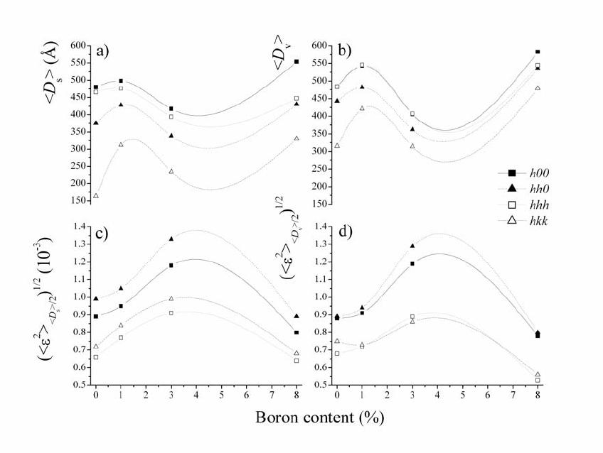 Vol.5, No.2 Structural and Microstructural Characteristics 151 illustrations of diffraction-line broadening measurements are shown in Figures 2 and 3. Figure 2. Graphic illustrations of crystallite: a) surface-weighted domain sizes, b) volume-weighted domain sizes, and c) RMSM averaged over the distance <D>s, d) RMSM averaged over the distance <D>v obtained by Warren- Averbach method. CONCLUSION The achieved results of structural and microstructural measurements, par exellence unit-cell and microstrain parameters indicate that B atoms embedding did not generate disorder in PbTe-type structure. The disorder increases until the sample has been doped with 3 % and then rapidly falls down with the sample doped with 8 % of B. So, if contents of B atoms in the PbTe structure were limited they would be expelled as an 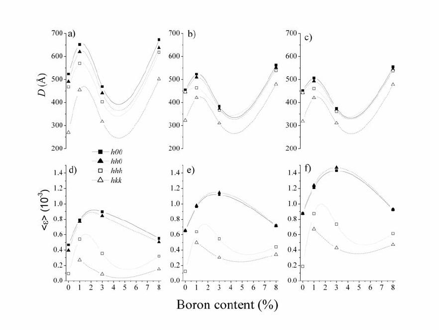 152 Stojanovic Vol.5, No.2 Figure 3. Graphic illustrations of volume-averaged domain sizes: a) Cauchy-Cauchy function, b) Cauchy-Gauss function, c) Gauss-Gauss function, and upper limit of microstrains: d) Cauchy-Cauchy function, e) Cauchy-Gauss function, f) Gauss-Gauss function obtained by the simplified integral- breadth methods. extra phase in the sample doped with 8 %. Have B atoms occupied interstitial site-positions or filled-up vacancies or maybe both? Since these are real crystals, the crystal lattice defects are expected to appear. Schottky-type defects appear when atoms or ions are of approximate dimensions; consequently, the atom distribution in interstitial site-positions is difficult one. Frenkel-type defects consist of either interstitial atoms or ions and vacancies in a crystal lattice. Small cations and big anions are favoured for this type of defects. The foremost assumption is that B atoms, mostly already filled-up, formed vacancies in layers with the highest microstrain Vol.5, No.2 Structural and Microstructural Characteristics 153 parameters: [h00] and [hh0]. Since Pb and Te atoms are of approximate radii, Schottky-type defects are expected. This means B atoms sited unattended vacancies. Considering B atomic radius, which is in comparison to Pb and Te atoms very small one, a certain amount of B atoms must have sited interstitially into the structure. Higher values of isotropic displacement parameters of doped samples in comparison to the pure one can be explained in the manner that B atoms increased overall values of Pb and Te atoms. So, the crucial conclusion is that B atoms predominantly filled- up vacancies and, to less extent, degree sited into PbTe structure interstitially. ACKNOWLEDGMENTS The authors are gratefully acknowledged to Professor Stevan Đurić and academician Pantelija Nikolić, who donated the samples and his associates from the Serbian Academy of Sciences and Arts for their thorough comments and suggestions, which significantly improved this paper. REFERENCES [1] BALZAR, D., LEDBET TER, H., 1997, “Software for comparative analysis of diffraction – line boadening.” Advances in X – ray analysis, vol. 39, edited by V. Gilfrich et al., Plenum Press, New York, pp. 457 – 464. [2] RODRIGUEZ – CARVAJAL, J., 1995, “User’s guide to program FULLPROF.” 2004-LLB- JRC (Laboratorie León Brillouin, CEA-CNRS, Centre d’Etudes de Saclay, Gif sur Yvette, France). [3] YASUTOSHI, N., SHIGERU, O., SHOISHI, S. & YOSHIHIKO, S., 1983, “Charge distribution and atomic thermal vibrations in lead chalcogenide crystals.” Acta Cryst., B39, pp. 312 – 317. [4] YASUTOSHI, N., KATASHI, M., SHOISHI, S., YOSHIHIKO, S., KOSHIRO, T & IWAO, I. 1987, “Temperature dependence of atomic thermal parameters of lead chalcogenides, PbS, PbSe, PbTe.” Acta Cryst., C43, pp. 1443 – 1445. |