 World Journal of Nano Science and Engineering, 2012, 2, 58-87 http://dx.doi.org/10.4236/wjnse.2012.22010 Published Online June 2012 (http://www.SciRP.org/journal/wjnse) Interface Recombination & Emission Applied to Explain Photosynthetic Mechanisms for (e–, h+) Charges’ Separation Marco Sacilotti1,2, Denis Chaumont2, Claudia Brainer Mota1, Thiago Vasconcelos3, Frederico Dias Nunes3, Marcelo Francisco Pompelli4, Sergio Luiz Morelhao5, Anderson S. L. Gomes1 1Department of Physics, Federal University of Pernambuco, Recife, Brazil 2Nanoform Group ICB & UFR Science and Technology, University of Burgundy, Dijon, France 3Departament of Eletronics and Systems, Federal University of Pernambuco, Recife, Brazil 4Plant Physiology Laboratory, Department of Botany, Federal University of Pernambuco, Recife, Brazil 5Institute of Physics, University of Sao Paulo, Sao Paulo, Brazil Email: msacilot@gmail.com Received January 31, 2012; revised March 3, 2012; accepted March 17, 2012 ABSTRACT To copy natural photosynthesis process we need to understand and explain the physics underneath its first step mecha- nism, which is “how to separate electrical charges under attraction”. But this Nature’s nanotechnological creation is not yet available to the scientific community. We present a new interpretation for the artificial and natural photosynthetic mechanism, concerning the electrical charges separation and the spent energy to promote the process. Interface (e–, h+) recombination and emission is applied to explain the photosynthetic mechanisms. This interpretation is based on energy bands relative position, the staggered one, which under illumination promotes (e–, h+) charges separation through the action of an interface electric field and energy consumption at the interface of both A/B generic materials. Energy band bending is responsible by the interface electric field (and the driving force) for the charges separation. This electric field can be as high or above that for p-n semiconductor junctions (104 - 105 V/cm). This physical effect is not considered by most of the researches. Without an electric field and without spending energy to separate electrical charges, any other existing model violates physical laws. The staggered energy band type is the only energetic configuration that permits charges separation under illumination and energy loss to perform the process. Application to natural photosynthesis and artificial photovoltaic material and their energetic configurations are discussed. Examples for A/B being III-V/III-V, TiO2/materials and II-VI/II-VI staggered energy band gap pairs are presented. In the proposed quantum mechanism, plants are able to eliminate most of the 79% of the absorbed visible light, according to the published reflection and transmission data. Moreover, the proposed mechanism can be applied to explain green fluorescent protein—GFP, charge transfer states—CTS and Fluorescent Resonance Energy Transfer—FRET. As recent literature experimental results propose photosynthesis as a quantum controlled mechanism, our proposition goes forward this direction. Keywords: Solar Energy; Renewable Energy; Photovoltaic; Photosynthesis; Type II Interfaces; Staggered Interface; Interface Emission; Interface Recombination; Quantum Photosynthesis; Solar Cell; FRET; GFP 1. Introduction Synthesis using light is the literal meaning of photosyn- thesis. It is the process by which plants are able to collect electromagnetic energy, mostly solar energy, that is used by organisms to synthesize complex carbon compounds. More specifically, light energy drives the synthesis of carbohydrates, which are essential for life. Thus, life on Earth ultimately depends on energy derived from the sun. Moreover, renewable energy is one of the most important scientific and technological topics on the current days, and a large fraction of the planet’s energy resources results from photosynthetic activities in either present or ancient times (fossil fuels). Photosynthesis first step, which is light absorption and separation of charges undergoing attractive electrical forces, is the most important physical/biological mecha- nism and should be copied in artificial systems such as solar cells. Therefore, photosynthesis must be understood at level of first principles, and based on physical para- meters since photosynthesis is nothing more than a com- plex physical process [1-3]. Life started on Earth 2 - 4 billions of years ago, when the first two or more molecules got together, probably in a puddle of water, absorbing light from the sun and sepa- C opyright © 2012 SciRes. WJNSE  M. SACILOTTI ET AL. 59 rating both charges (e–, h+), perhaps catalysed by other factor as discharge and/or with the mineral environment participation. Since its first occurrence, this mechanism and the evolution of species on Earth gave us only one catalytic mechanism to separate oxygen from water [1]. The oxygen separation is one of the subsequent steps after the charges separation on photosynthesis’ processes. In the early days of Earth’s exuberant vegetation, most of the available atmosphere gases were CO2 and N2. O2 had appeared with the evolution of the charges separation process. Nowadays we have increased the CO2 level from 200 (~1850) to 370 ppm (~2010) [1-3]. It has been an important point for scientists looking for renewable energy sources, and one of the issues is to copy the natural photosynthesis approach, related to the (e–, h+) electrical charges separation mechanism. The absorption of light by organic molecules or inorganic nanomaterials doesn’t provide the electrical charges separation directly. This is just the first part of the process. If the material absorbs light, the following step is its recombination within the same material, releasing energy related the material’s band gap energy (the forbidden band). To have (e–, h+) charges separation requires a suitable energetic configu- ration of the band gaps to allow the generation of the necessary electric field to separate the (e–, h+) pair. This electric field should arise from a potential variation. The mechanism that separates electrical charges of different polarities will be interpreted and described here. The expression “separation of charges of different polarities” means the separation of negatives, e–, from positives, h+, electrical charges, which undergo an electrical attraction called excitonic attraction. An appropriate electric field is necessary to break the excitonic attraction, i.e. to split both (e–, h+) charges, and hence energy must be spent. Any model that do not account for the electric field and the spent energy are violating physical laws. Our pro- posed model accounts for both: the necessary electric field and the spent energy. Furthermore, it seems to be the only energetic configuration capable of providing charges separation under excitation of light, and it is based on staggered energy band gaps between two dif- ferent materials of nanometric dimensions. At the interface, A/B, between generic materials A and B, there are naturally three possible energetic configura- tions of the band gaps: type I, type II and type III [4-12]. Type I interface are largely applied to construct solid state LEDs, laser, and most of the optoelectronics devices [10]. Type I energetic interface can be represented when- ever the energy band gap of one material is inserted within the band gap of the adjacent material. Type III energetic interface occurs when the band gaps do not over- lap [4-8,10]. Only the type II interface, the staggered one, shown in Figure 1 will be discussed here, concerning its excitation by light and the bending of its valence and Figure 1. Flat band configuration for A and B materials staggered generic interface, representing the conduction band (CB or LUMO) and valence band (VB or HOMO). Note electrical charges (e–, h+) have always energetic steps (electric potential barriers up or down) when travelling from A to B or from B to A. This energy flat band configu- ration is a non-excited system; otherwise it should be band bended. conduction energy bands. The band bending effect is caused by charges falling down to lower levels of energy states, creating a dynamic electric field that allows both (e–, h+) charges separation [4,10,12]. This paper is organized as follows. An introduction to type II interface and examples of applications on AlInAs/ InP semiconductor system and other systems such as TiO2/II-VI and II-VI/II-VI, emphasizing their very effi- cient mechanism for photon emission due to recombine- tion of e– and h+ charges seated on different materials. Intriguing results on reflection and transmission, avail- able on specialized literature for plants, will be discussed, for the first time, under the scope of physical principles. These discussions concern transmission and reflection experiments that give about 79% of absorption for natural leaves at the visible spectral region. Such very high pho- ton absorption should “fries” leaves in few minutes in the absence of a fast optical emission mechanism to throw away much of the absorbed energy. We propose here that natural photosynthesis and artificial photovoltaics (nano- metric systems) should be regarded as a quantum-con- trolled mechanism, differently of the currently accepted model, based on classical physics [1-10,13]. The present proposal provides both: the necessary electric field and the spent energy to separate negative from positive charges. It will be applied and discussed for both inor- ganic and organic systems. As explained below, the ener- getic relative position between two different materials is not a controversial question because modern organics LEDs and organic solar cells devices uses this concept. Moreover, many experimental results on energetic rela- tive position and energy band bending on organics do exist, excluding the frequent “controversial” argument to avoid new ideas and explanation of the physical phenomena. Copyright © 2012 SciRes. WJNSE  M. SACILOTTI ET AL. 60 2. Current Representation of Energy Band Offsets between Natural Organic Materials Photosynthetic’ natural light reactions are represented by energy bands of different molecules that absorb light and transfer its energy to others molecules. This energetic representation is called “ground state energy” (GSE) [13-15]. According to Bjorn et al., the energetic relative position for molecules on leaves is unknown [15]. If it is unknown, experimental data should be performed to know their offset to get to actual scientific systems. The distribution of charges on excited organic molecules is somewhat different from the distribution represented on the GSE model. Unfortunately the GSE model, or repre- sentation, does not apply to any actual physical configu- ration; it leaves no room for feasible charge separation mechanisms in natural photosynthetic process. Existing electrical charges travelling from one to another different material have always energetic steps (up or down). The GSE energetic representation can not promote charges separation since there is no driving force to break the excitonic attraction [4,7,12]. Without the driving force, the GSE model and energy transfer mechanism model fails (see the discussion below, about fluorescence reso- nance energy transfer—FRET and green fluorescent pro- tein—GFP). According to current believes, leaves are green to human eye due to chlorophyll molecules that absorb light mainly in the red and blue ranges of the visible spectrum; hence only light enriched in green wavelengths (about 535 - 550 nm) is reflected from leaves to our eyes [2]. However, there is no direct proof that the green colour of leaves is mostly due to reflection. In addition, there is no physical reason to explain why the leaves’ colours are not related to emission. Note that leaves are de-pigmented (i.e., absence of green colour) when light is turned off. Equally, as presented below, excitation of leaves with green or higher energy photons gives many other colours’ emissions. As it will be com- mented bellow, organic solar cells and organic LEDs, composed of nanometer thin layers, uses the concept and experimental results of staggered energy band gap con- figuration, in contrast to the GSE configuration. As GSE is not feasible in physical systems, the staggered band en- ergy configuration (Figure 1) provides the major benefit for the light reaction of photosynthesis: the electric field (driving force) for (e–, h+) electrical charges separation. At the interface, the electric field comes from the nearby A/B materials interface energy band bending (Figure 2), and the interface light emission can be related to the spent energy, associated to the charges separation. In conclusion for this section, organic molecules pre- sent on leaves should experiment energetic (or potential) steps for electrical charges movements between them. Without these energetic steps it is impossible to propose a mechanism for charges separation for the natural and Figure 2. Type II interface representation under light exci- tation of both A and B materials and the interface energy band bending on both sides. These energy band bending are created by the e– and h+ charges falling down to the lower energetic steps at the interface (including possible tunnel- ling of charges). The interface energy band bending creates electric fields on both sides, responsible for the charge sepa- ration to the opposite interface’s directions (the driving force F− & F+). h i represents the interface photons energy emission, related to the spent energy to separate (e–, h+) charges under excitonic attraction. The interface energy band bending (or the electric potential) gives rise to the electric field EiA & EiB. Note that the h i interface emission is also issued from a tunnelling mechanism. Eext is the ex- ternal electric field applied to the AlInAs/InP structure, as explained in the text, to decrease the h i emission intensity. artificial photosynthetic processes. By using non-existing physical energetic configuration (e.g., the GSE configu- ration) we fail in explaining the physical mechanisms. Any model based on non-existing energetic configuration bring us to violate physical laws whenever trying to ex- plain the physical mechanisms. The light absorption by molecules within leaves is only the first step of the proc- ess and it does not separate e– from h+. The next step, to separate e– from h+, depends on the energetic configure- tion between the existing molecules within the leaves. Type II (staggered) energetic interface is proposed to overcome the problem. Copyright © 2012 SciRes. WJNSE  M. SACILOTTI ET AL. 61 3. Current Energy Band Offsets Representation between Inorganic Materials The artificial photosynthetic mechanism (applied to modern solar cells) is currently and conveniently repre- sented by type II interfaces (the staggered one, repre- sented in Figure 1) [16-21]. But the model frequently fails because the semiconductors interface band bending phenomena is not considered, whenever charges fall down to lower energy levels at the interface between two A/B generic materials [4-7,10,16-21]. Only the flat band configuration is considered for most of the artificial pho- tosynthetic process. With no energy band bending con- siderations, there is no electric field (driving force) to separate both charges of different signals, as represented in Figure 2. The staggered energetic representation for artifi- cial photosynthesis does not consider that the falling down of electrical charges at the interface is a sink for them [16-29]. Once these charges cross the interface, they re- combine there and they are lost because the recombine- tion gives rise to interface emission [7,9,23-29]. This in- terface recombination is erroneously and frequently called charge transfer state (CTS) [27-29]. The authors do not understand why the expression “charge transfer state” is applied, since it is simply interface recombination and emission. These CTS are applied to organic and inorganic systems and it will be discussed below in more details. Note that both natural and artificial photovoltaic mech- anisms described above are dynamic systems, as repre- sented in Figure 2. It is the near interface electric field; created by the electrical charges falling down, that sepa- rates e– from h+ [4-7]. This interface electric field arises from a varying potential (or energy band bending). Without illumination the flat band condition takes place, as presented on Figure 1. As soon as (e–, h+) pairs are no longer created (no excitation), there are no longer electrical charges falling down to lower energy steps at the interface. Without light, the equilibrium condition is achieved and there is no more interface energy band bending (no electric field, able to separate e– from h+, as presented in Figure 2). At this moment, the interface light emission stops. Note that the consumption of (e–, h+) pairs at the interface (by interface emission) brings the A/B system to equilibrium, without external excita- tion. As the present proposal represents a different regard on photosynthetic systems, it will be described below step by step, bringing the necessary physical tools and experimental proofs of its existence. In conclusion for this section, inorganic photovoltaic nanomaterials present the actual band offset (the stag- gered one), but suffers from the mains physical tools to separate electrons from holes: the necessary electric field and the spent energy to separate electrical charges under attraction. The physical laws’ violation is twofold in this case, even though the experimental results are very im- portant for solar energy developments. The physical me- chanism to separate (e–, h+) is not present. 4. Physical Principle of the Charge Separation Mechanism According to the Nobel Prize Laureates L. Esaki (1973) and H. Kroemer (2000), the staggered energetic configu- ration between two different A/B materials, the flat band configuration (no excitation), is presented in Figure 1. This representation is only for the conduction band (CB or LUMO) minima and valence band (VB or HOMO) maxima at the momentum configuration (K space) [4-7, 10]. These minima and maxima are related to parabolic energetic representation of energy on K space [10]. Under A and B light excitation, it takes the configuration showed in Figure 2 where we can observe: (e–, h+) pairs genera- tion; e– and h+ jumping to lower energetic steps at the interface and, consequently, the energy band bending of both bands CB and VB in both A and B materials. Such jumping of charges leaves both materials into a non-equi- librium electronic state. Note that the jumping of charges to the nearby material put both A and B materials under non-equilibrium electronic condition [4,8,10]. This non- equilibrium electronic condition should move both quasi- Fermi energy levels on both sides of the interface. Mov- ing both quasi-Fermi energy levels, should move (bend) both CB and VB on both sides of the interface [4,7,10]. The interface energy band bending creates barriers for few remaining electrons and holes (at the CB and VB of both materials). These few remaining charges are no longer allowed to go across the bended barriers. Their thermal energy is not enough to promote tunneling across these barriers. The electrical charges are therefore sent away from the interface by the gradient of the electric potential (the electric field being E = –grad V). They represent the separated charges by the energy band bend- ing action (and by the interface created electric field on both sides of the interface) [4,10]. The (e–, h+) that fall down to the lower interface energy steps recombine at the interface, giving rise to the interface recombination and photons emission (h i). These emitted photons are lost, representing a faster and easier way to efficiently waste photon energy for A/B generic systems. Interface energy band bending is frequently used as a result of charges falling down to lower available energy levels [4, 7,10]. As the interface electric field (EiA, EiB, Figure 2) comes from the potential variation at both sides of the interface, we have the necessary electric field and the driving force to separate electrons from holes. Note that potential variation and energy band bending are related, since energy = potential × electrical charge. Shortly, most of the excited charges jump, creating the band bending, and few excited charges do not achieve to cross the barriers Copyright © 2012 SciRes. WJNSE  M. SACILOTTI ET AL. 62 created by those crossing the interface. A support infor- mation file represents the proposed mechanism, for a generic A/B interface, excited with only four photons, in a slow motion representation way [SI-1]. The interface energy band bending is not frequently considered on photovoltaic artificial experiments and conclusions [16-21,27-29]. Without the energy band bending there is no interface electric field. Without an interface electric field (both, EiA and EiB, in Figure 2), (e–, h+) charges do not get separated. Note that energy band bending and Fermi level movement follow each other [10]. On nanostructured materials their size is too small to consider diffusion controlled mechanism [10, 16-22]. Carriers’ diffusion length on bulk materials is many orders of magnitude of that of the size encountered on nanosized materials [10,22]. In this way the charges separation explanation and the charges displacement di- rection are not physically correct in many published pa- pers [16-21,27-29]. On the other hand, the dynamical bending of the energy bands (and Fermi level), as pro- posed here, is perfectly in agreement with all physical concepts, providing the fundamental theoretical explana- tion on how charges get separated on such systems, as detailed below for TiO2/II-VI and II-VI/II-VI semicon- ductors systems [4,10]. To each (e–, h+) recombination at the interface, a photon of energy h i, ieh hSQQ x E (1) is emitted (Figures 2 and 3). ∆S is the overlap of the energy bands of the A and B materials without excitation, i.e. in the flat band configuration (Figure 3); ∆Qe is the electron energy quantization within the interface quasi- triangular shape quantum well; ∆Qh is the hole energy quantization within the interface quasi-triangular shape quantum well and ∆Ex is the electron-hole excitonic in- teraction energy. Note that h i, the interface energy emission, is always lower than both A and B band gap materials. So, material B band gap energy > h i < mate- rial A band gap energy. This can explain many lower energy peaks on composed type II interfaces presented in the literature, but not understood up to now [16-29]. As already mentioned, this interface photons emission is erroneously called charge transfer state [27-29]. But it is just an interface (e–, h+) recombination and emission. This energy is lost but it is at the origin of the band bending and interface electric field. Figure 3 represents the energy balance at the A/B sys- tem when excited by photons with enough energy to promote electrons from the VB to the CB on both A and B materials. By exciting the A and B materials, the fal- ling down of electrons from B to A increases the inter- face electron density, represented by ∆Qe (negative elec- trical charges on A). In the same way, the falling down of Figure 3. Energy balance at the A/B interface. The observed interface photon emission is represented by h i, which de- pends on S, the non excited A/B energy band gap overlap, the Qe, electron quantized well energy, the Qh, holes quantized well energy and the Eex, electron-hole excitonic energy. Note the interface energy band bending depends equally on the h , the photon external excitation energy. Equally, Qe & Qh depend on h . holes from A to B increases the interface holes density, represented by ∆Qh (positives electrical charges on B). As a consequence of a high density of opposite sign elec- trical charges at the interface, a high ∆Qe and ∆Qh inter- action appears. Note that both quasi-Fermi level should follows these charges movements [10]. This high (e–, h+) interaction at the interface, represented by ∆Ex, the exci- tonic interaction between e– and h+, ∆Ex, is of the order of few to tens of meV for bulk semiconductor materials. ∆Ex is of the order of hundreds of meV for organic mole- cules [10,22]. This ∆Ex physical energy parameter for (e–, h+) interaction (but seated on different materials) gener- ates a strong interface emission (electrical charges wave function barrier penetration or tunneling). It is important to register that the ∆Ex value have never been presented in the literature for (e–, h+) pairs seated on different ma- terials, for type II (staggered) interfaces recombination and emission, represented by h i [10,22]. Note that the falling down of e– and h+ to the nearby material should move quasi-Fermi level meanwhile band bending takes place. Electrons leaving material B (Figures 2 and 3), the quasi-Fermi level should go down on ma- terial B. Holes leaving material A, the quasi-Fermi level should go up on material A [10]. Both ∆Qe and ∆Qh cre- ate an interface electric field from the material B to the material A. It has the same direction of both EiA and EiB on Figure 2. Note also that the Fermi level (no excitation, Figure 1) depends on the materials doping conditions Copyright © 2012 SciRes. WJNSE  M. SACILOTTI ET AL. 63 and the quasi-Fermi levels depends on doping and exter- nal excitation (Figures 2 and 3) [10]. This question will be discussed below for the AlInAs/InP system and pre- sented at the support information 1 [SI-1]. Figure 4 represents an A/B interface composed by a staggered excited system, with both exponential (quasi- triangular) shape quantum wells for electrons (material A) and holes (material B). The wave functions probabilities for the (e–, h+) pairs are equally represented. Calculus (Support Information 2 [SI-2]) were performed for the InP/AlInAs system and based on physical parameters available in the literature [23]. Details of the calculus for the (e–, h+) wave functions overlap, energy band bend- ing and existing electric field at the InP/AlInAs interface is presented elsewhere [23, 30 and in SI-2]. In this work (Figure 4) the energy bands are modelled as exponential bended bands, leading to Bessel wave function for carri- ers. Energy levels of carriers at valence and conduction bands, as well as the penetration depth, for each kind of carrier are obtained by solving the transcendental equa- tion obtained for wave function continuity at the inter- face. Note in Figure 4: electrons have one and holes have two wave functions probabilities representation. The wave function probabilities with about 2 nm and 1 nm of barrier penetration, respectively for e– & h+, are repre- sented in this Figure 4. Both barriers wave function penetration are enough to explain the strong interface photons emission discussed below and presented on Figure 5. The barriers wave function penetration and the strong interface emission observed by the authors and many others research groups corroborate our comments on type II interface physical parameters [12,19,23-25, 27-29]. Note that this interface quantum controlled me- chanism (wave function penetration, tunnelling) is valid for II-VI and for III-V A/B generic materials’ interfaces [16-21,23-25,27-29]. Interface recombination is a dynamical quantum proc- ess and a very efficient emission mechanism. As the light excitation intensity upon the system increases, the elec- tron cascade from upper to lower CBs energy levels, en- hancing the band bending effect. So, the interface emis- sion is liked and responsible for the CB and VB energy band bending and it is also associated to the spent energy for the charges separation, represented in Figure 2. The falling down of electrical charges at the staggered inter- face creates the band bending on both sides of the A/B system (Support Information 1 [SI-1]). The charges fal- ling down increase ∆Qe and ∆Qh values and the interface emission. As a consequence there is also an increase at the quasi-triangular shape well deepness (represented by the energy band bending in Figures 2 and 4) at the same time. By increasing the well deepness, it increases the interface PL intensity and broadens the interface peak emission, h i. It also increases the (e–, h+) wave function barrier’s penetration and tunneling. The intensity and broadness of the interface emission, as discussed below, occurs due to the lack of QM selection rules. The inter- face light emission is a very efficient (e–, h+) recombine- tion mechanism [23-25,27-29]. Note that the effect is double on each side in both sides (leaving e– and receiv- ing h+), increasing band bending (or increasing the in- terface electric field EiA & EiB). The low efficiency of the presented model for charges separation mechanism cor- roborates and can explains the low efficiency of natural and artificial systems (1% - 6%). This is the reason for most of the photons energy loss at the interface and the movement Figure 4. A/B material excited interface, presenting the CB band energy bending for electrons and its quantum well energy levels, and the VB band energy bending for holes and its quantum well energy levels. X represents the dis- tance from the interface in nanometer (nm); h i, the photon interface emission following the (e–, h+) interface recombi- nation; and P(x), the (e–, h+) wave function probability to be found on A or B. Note there are two holes wave function probability for the conditions we use for the simplified cal- culations [30 and SI-3]. As the energy band bending de- pends on the photon energy excitation, many energy levels are expected on these wells, owing to the spectral FWHM width presented in Figure 5 (34 to 36 meV at 77K). The P(x) value penetration for holes on A is about 1 nm; for electrons on B it is about 2 nm. These values are enough to account for the interface intense emission PL peaks observed in Figure 5 (1.303 and 1.193 eV). Similar results are presented on references [23-25,27-29]. Copyright © 2012 SciRes. WJNSE  M. SACILOTTI ET AL. 64 Figure 5. 77 k photoluminescence (PL) intensity (I) versus wavelength experimental results of an InP/AlInAs/InP (A/B/A) energy staggered interface. Both interface emissions (1.303 and 1.193 eV) are very intense and broad, compared to the bulk InP (1.395 eV) and bulk AlInAs (1.499 eV) emissions. These InP and AlInAs PL emissions are observed due to the ternary layer thickness (1.6 µm), above the carriers mean free path diffusion length (allowing AlInAs CB-VB transitions and observation) and the binary layer thickness top layer (0.1 µm, allowing InP CB-VB transitions and observation) [9,23,24]. Both materials are intrinsically n-type doped (AlInAs ~1016 at/cm3, InP ~1015 at/cm3). of few e– and h+ away from the interface (in opposite directions). Moreover, it is a quantum-controlled system as it will be exemplified below, for inorganic/inorganic A/B systems, and as proposed for the photosynthesis modern experiments. In conclusion for this section, the necessary physical tools to separate e– from h+ and recombination at a type II interface energetic configuration is presented. It is based on an existing energetic configuration, already described for inorganic materials. Whenever electrons jump from material B to material A (Figures 1-3), they leave mate- rial B under excess of holes and under electronic non- equilibrium condition. This non-equilibrium condition moves the quasi-Fermi level down and conduction band moves up on material B. Whenever holes jump from a material A to a material B, they leave material A under excess of electrons and under electronic non-equilibrium condition. This non-equilibrium condition moves the quasi- Fermi level up and the valence band down on material A. Most of the excited A/B interface charges recombine when jumping, but this event has created a gradient in the elec- tric potential and an interface electric field. As the jumped charges are lost and emitted as h i, their act promotes the necessary condition to separate few non-jumped electrical charges. In this case we have both physical tools to sepa- rate e– from h+: the electric field and the spent energy, without violating physical laws. 5. Application to the InP/AlInAs/InP Staggered System The III-V semiconductors can be easily grown through the metal-organic chemical vapour phase (MOCVD) technique [9,23-25]. The InP/AlInAs system has a stag- gered energy band gap relative position [7,9,23-25]. As a staggered A/B system, it presents an interface h i strong emission. The A and/or B band gap emission observation (bulk material) depends on the layers thicknesses, when- ever A/B interface is grown. For an InP/AlInAs thin film thicknesses (below carriers diffusion length << 1 µm), the optical response presents only the interface emission, which energy is about 1.193 eV [9,23,24]. For thicker films (above carriers diffusion length, ≥ 1 µm), the inter- face emission is still the predominant optical phenomena. Figure 5 presents the photoluminescence of an InP/ AlInAs/InP system, where two staggered interfaces are present. The one called direct: AlInAs grown on InP (with a 1.193 eV emission peak) and the one called inverse interface (InP grown on AlInAs, 1.6 µm thick, with a 1.303 eV emission peak) [9,24]. Both interface peaks’ emission are broad (34 - 36 meV at 77 k and 70 - 80 meV at 300 K) and intense, characteristics of type II in- terface emission. These broad energy peaks are related to the ∆Qe and ∆Qh available energetic states presented in Figures 3 and 4 and Equation (1). As (e–, h+) are located in different materials, the recombination occurring at the interface takes place free of any quantum mechanical k selection rule (k = momentum), following the lack of lattice periodicity (e– and h+ are seated on different ma- terials). This fact improves the probability of recombine- tion, making it a more efficient mechanism, as observed in Figure 5. As the MOCVD growth conditions does not allow ease change from As to P chemical elements, the InP growth on AlInAs possess a much wider transition inter- face and, consequently, the bands offsets are not the same as for AlInAs grown on InP. The inverse interface has an InAsP (about 6 nm) transition layer, as stated by Auger spectroscopy [9]. These results proof, even with non-optimised (non-abrupt) staggered interface, the in- terface recombination mechanism is still predominant for 0.1 to 1.6 µm tick AlInAs layers [9,23-25]. For nano- sized materials these effects should be much more pro- nounced, as it occurs with TiO2/II-VI semiconductors materials applied to solar cells research [26-29]. The laser excited AlInAs/InP direct interface fluorescence, with 1.193 eV energy peak emission, shown in Figure 5, creates the Copyright © 2012 SciRes. WJNSE  M. SACILOTTI ET AL. 65 energy band bending on both sides of the interface. These energy band bending (or varying electric potential) can be evaluated by solving Poisson’s equation on both sides of the interface (see support information 3 [SI-3]). A simple estimation (not shown) for the (e–, h+) dyna- mic electric field is from 0.4 × 10⁵ V/cm (EiB, material B = AlInAs) and 1.24 × 10⁵ V/cm (EiA, material A = InP) [25,30,31,SI-3]. To decrease the interface PL (measured at 12 to 77 K) 1.193 eV intensity to zero, an external electric field of about 105 V/cm should be necessary, represented in Fig- ure 6 [25,31]. This is the physical condition to cut off (stop interface emission) the charge falling down to lower energy steps of the present AlInAs/InP structure. Sur- prisingly this is approximately the electric field necessary to decrease to zero the interface emission intensity of a similar AlInAs/InP structure published by Sakamoto et al. ([25], its Figure 1, PL intensity extrapolated to zero, plotted as a function of the external applied electric field, which value is 0.55 × 10⁵ V/cm) [31]. Our PL experi- ments shown in Figures 5 and 6 are in accordance with the results of Sakamoto and co-workers and reveal how important is the existing high value electric field at the excited type II interface [9,23-25,31]. Note that this elec- tric field is comparable to the p-n Silicon semiconductor junction electric field (104 to 105 V/cm) [10]. Attention should be taken because it is compared to the extrapo- lated 12 K and 77 K electric field values [25,31]. The error percentage is low between 12 K and 77 K [10]. Compar- ing the estimated electric field (caused by band bending at the AlInAs/InP interface, 77 K) with that of a Silicon p-n junction ( about 104 - 105 V/cm, at 300 K) it gives an idea about the dimension of the excited type-II interface electric field, as exposed in Figure 6 [10,30,31]. This comparison is proposed only to give the order of magni- tude of the AlInAs/InP excited interface electric field. Moreover, the order of magnitude of a light excited AlInAs/InP type II interface electric field is known for the first time [10,25,31]. Note that Figure 6 presents results of the clear proof of the interface electric field at a type II, staggered excited interface. These EiA and EiB (Figure 2) interface electric fields, added because they are in the same direction, issued from CB and VB band bending (due to the jumping of e– and h+ at the interface) are responsible by the few others e–, h+ running to the opposite side of the interface. They are the separated charges by type II interface (the driving force, F− & F+ represented in Figure 2). As it will be mentioned below, to the staggered model, applied to organic molecules (chlorophyll in leaves, for the photosynthesis mechanism), the interface dynamic electric field should be much more pronounced because of the nanometer size dimension and distances within the Natural system in plants. Note that electric field depends ~0.55 × 10⁵ 0.2 0.4 0.6 (× 105 V/cm) Figure 6. Top: explored structure. Botton: PL intensity (I) versus external applied field. Experimental results on type II interface emission (1.2 eV, at 12 K) for an AlInAs thin layer (100 nm) grown on InP. The PL peaks were withdraw from [23-25]. Applying an external electric field to the structure (Eex), the interface emission (h i) reaches zero intensity. For this structure, as the AlInAs thickness is be- low the charges diffusion length, we observe only the inter- face emission peak; InP and AlInAs peaks are very low intensity. This experiment shows that energy band bending gives rise to the interface electric field (Ein), able to separate e− from h+. Application of an external electric field (Eex) to the AlInAs/InP structure, the 1.2 eV interface emission goes to zero with Eex ~0.55 × 10⁵ V/cm (Eex cancel Ein) [25]. This is the clear proof of the interface electric field (Ein) related to the potential variation (band bending) and interface emission. Note that the 1.2 eV interface emission peak moves to lower energy as Eex increases, as Qe and Qh decreases (Equation (1) and [25]). inversely on the square of the distance between two elec- trical charges. These results are applied to organic systems, as already published, to produce type II energetic inter- faces for LEDs and organic solar cells, discussed below. Fortunately, recent publication on organic LEDs and organic solar cells use experimental results of type II interface. Unfortunately energy band bending is not fre- quently applied to organic devices. In contrast, natural photosynthesis models fail on scientific physical basis Copyright © 2012 SciRes. WJNSE 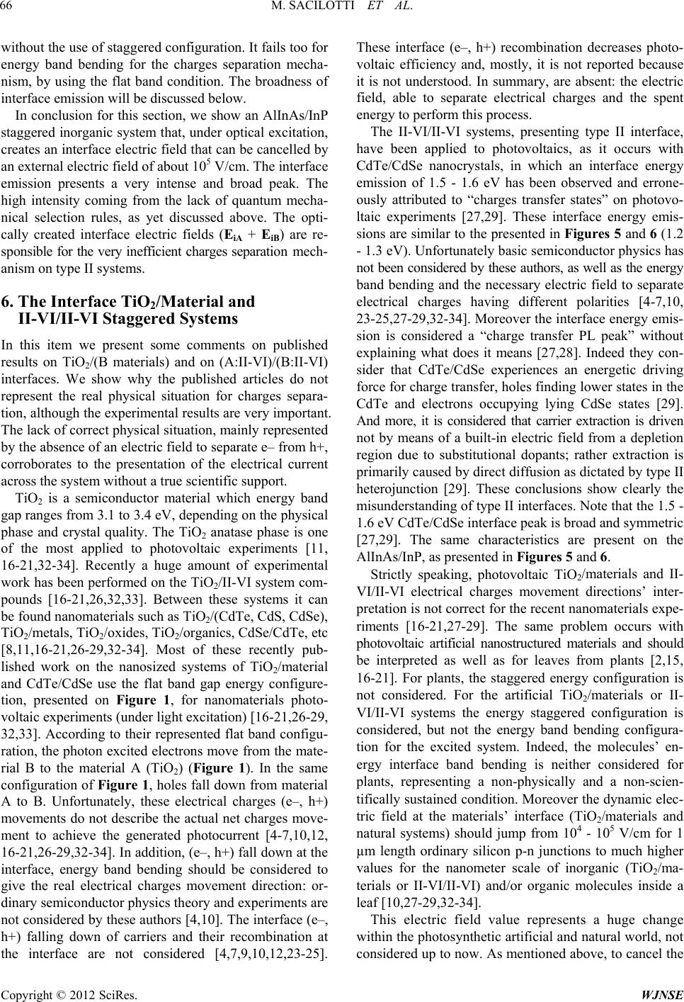 M. SACILOTTI ET AL. 66 without the use of staggered configuration. It fails too for energy band bending for the charges separation mecha- nism, by using the flat band condition. The broadness of interface emission will be discussed below. In conclusion for this section, we show an AlInAs/InP staggered inorganic system that, under optical excitation, creates an interface electric field that can be cancelled by an external electric field of about 105 V/cm. The interface emission presents a very intense and broad peak. The high intensity coming from the lack of quantum mecha- nical selection rules, as yet discussed above. The opti- cally created interface electric fields (EiA + EiB) are re- sponsible for the very inefficient charges separation mech- anism on type II systems. 6. The Interface TiO2/Material and II-VI/II-VI Staggered Systems In this item we present some comments on published results on TiO2/(B materials) and on (A:II-VI)/(B:II-VI) interfaces. We show why the published articles do not represent the real physical situation for charges separa- tion, although the experimental results are very important. The lack of correct physical situation, mainly represented by the absence of an electric field to separate e– from h+, corroborates to the presentation of the electrical current across the system without a true scientific support. TiO2 is a semiconductor material which energy band gap ranges from 3.1 to 3.4 eV, depending on the physical phase and crystal quality. The TiO2 anatase phase is one of the most applied to photovoltaic experiments [11, 16-21,32-34]. Recently a huge amount of experimental work has been performed on the TiO2/II-VI system com- pounds [16-21,26,32,33]. Between these systems it can be found nanomaterials such as TiO2/(CdTe, CdS, CdSe), TiO2/metals, TiO2/oxides, TiO2/organics, CdSe/CdTe, etc [8,11,16-21,26-29,32-34]. Most of these recently pub- lished work on the nanosized systems of TiO2/material and CdTe/CdSe use the flat band gap energy configure- tion, presented on Figure 1, for nanomaterials photo- voltaic experiments (under light excitation) [16-21,26-29, 32,33]. According to their represented flat band configu- ration, the photon excited electrons move from the mate- rial B to the material A (TiO2) (Figure 1). In the same configuration of Figure 1, holes fall down from material A to B. Unfortunately, these electrical charges (e–, h+) movements do not describe the actual net charges move- ment to achieve the generated photocurrent [4-7,10,12, 16-21,26-29,32-34]. In addition, (e–, h+) fall down at the interface, energy band bending should be considered to give the real electrical charges movement direction: or- dinary semiconductor physics theory and experiments are not considered by these authors [4,10]. The interface (e–, h+) falling down of carriers and their recombination at the interface are not considered [4,7,9,10,12,23-25]. These interface (e–, h+) recombination decreases photo- voltaic efficiency and, mostly, it is not reported because it is not understood. In summary, are absent: the electric field, able to separate electrical charges and the spent energy to perform this process. The II-VI/II-VI systems, presenting type II interface, have been applied to photovoltaics, as it occurs with CdTe/CdSe nanocrystals, in which an interface energy emission of 1.5 - 1.6 eV has been observed and errone- ously attributed to “charges transfer states” on photovo- ltaic experiments [27,29]. These interface energy emis- sions are similar to the presented in Figures 5 and 6 (1.2 - 1.3 eV). Unfortunately basic semiconductor physics has not been considered by these authors, as well as the energy band bending and the necessary electric field to separate electrical charges having different polarities [4-7,10, 23-25,27-29,32-34]. Moreover the interface energy emis- sion is considered a “charge transfer PL peak” without explaining what does it means [27,28]. Indeed they con- sider that CdTe/CdSe experiences an energetic driving force for charge transfer, holes finding lower states in the CdTe and electrons occupying lying CdSe states [29]. And more, it is considered that carrier extraction is driven not by means of a built-in electric field from a depletion region due to substitutional dopants; rather extraction is primarily caused by direct diffusion as dictated by type II heterojunction [29]. These conclusions show clearly the misunderstanding of type II interfaces. Note that the 1.5 - 1.6 eV CdTe/CdSe interface peak is broad and symmetric [27,29]. The same characteristics are present on the AlInAs/InP, as presented in Figures 5 and 6. Strictly speaking, photovoltaic TiO2/materials and II- VI/II-VI electrical charges movement directions’ inter- pretation is not correct for the recent nanomaterials expe- riments [16-21,27-29]. The same problem occurs with photovoltaic artificial nanostructured materials and should be interpreted as well as for leaves from plants [2,15, 16-21]. For plants, the staggered energy configuration is not considered. For the artificial TiO2/materials or II- VI/II-VI systems the energy staggered configuration is considered, but not the energy band bending configura- tion for the excited system. Indeed, the molecules’ en- ergy interface band bending is neither considered for plants, representing a non-physically and a non-scien- tifically sustained condition. Moreover the dynamic elec- tric field at the materials’ interface (TiO2/materials and natural systems) should jump from 104 - 105 V/cm for 1 µm length ordinary silicon p-n junctions to much higher values for the nanometer scale of inorganic (TiO2/ma- terials or II-VI/II-VI) and/or organic molecules inside a leaf [10,27-29,32-34]. This electric field value represents a huge change within the photosynthetic artificial and natural world, not considered up to now. As mentioned above, to cancel the Copyright © 2012 SciRes. WJNSE  M. SACILOTTI ET AL. 67 interface electric field of a light excited AlInAs/InP stag- gered system we need an external electric field about 0.55 × 10⁵ V/cm [25,31]. These physical principles rep- resent a just known simple semiconductor interface phy- sics, not considered up to now [4-10,12,23-25,31]. In conclusion to this section, type II interface, applied for TiO2/(B material) and A:II-VI/B:II-VI systems, uses the right energetic configuration but do not propose the necessary physical tools to separate electrical charges under attraction: the electric field (issued from the energy band bending) and the spent energy (issued from inter- face recombination). The flat band representation for excited systems does not hold on physical basis. Under photons excitation, the jumping of charges to the nearby material brings the near interface to a non-equilibrium condition on both A and B material’s electronic structure and, consequently, it brings the energy band bending (or potential variation) and the Fermi level movement (dyna- mic process). The interface recombination is erroneously attributed to “charge transfer states” that is not under- stood by the authors of the present work. Charge transfer states are confused with interface recombination and emission, related to the spent energy (loss) to separate e– from h+. 7. Why Is the Interface Emission So Broad In our model, the interface emission comes from two quasi-triangular quantum wells, representing energy states within ∆Qe and ∆Qh (Equation (1) and Figure 7). As the deepness of these quantum wells depends on the number of charges jumping to the nearby material and these numbers depends on the number of arriving photons, the emission peak (h i) will depend on both terms ∆Qe & ∆Qh. Moreover, without QM selection rules, charges on each energy level on ∆Qe is supposed to recombine with charges on each energy level of ∆Qh. It gives rise to the broad interface emission. Note that ∆Ex (excitonic attrac- tion, Equation (1)) should also be dependent on the opti- cal excitation intensity and on ∆Qe and ∆Qh. As guidelines for type II interface properties, the main characteristics of type II interface can be summarized as follows: 1) It is a very efficient (e–, h+) recombination quan- tum mechanical mechanism (but with no QM selection rules). Note: e– mobility >> h+ mobility, able to allow an interface permanent e– population inversion; 2) It is a very intense and efficient photons interface’s emission; 3) It has a very broad interface emission peak: h i = ∆S + ∆Qe + ∆Qh – ∆Ex (these quantities are explained on Figure 7). Note that the peak broadness, FWHM f (ex- citation intensity and excitation wave length); interface hv i emission = hv i = S + Q e + Q h - E x Q e Q h S Material A Material B hv i interface absorption is possible electron s holes Figure 7. Representation of the main characteristics of type II interface emission: two quasi-triangular shape quantum wells (QW) are present on opposite side of the interface and the energy levels in these QW. The luminescent interface peak is large and intense due to: (a) (e– & h+) are localized on two different materials on quasi-triangular shape quan- tum wells, on both sides of the interface; (b) The deepness of both A/B materials’ interface quantum wells, Qe + Qh, depends on the excitation density (number of arriving pho- tons); (c) Absorption and emission by the interface are pos- sible; (d) The excitonic interaction (Ex) and the e– & h+ wave function overlap should also depend on the excitation density. Note that the lack of quantum mechanics selection rules for (e–, h+) recombination at the interface is a conse- quence for both (e–, h+) seated on different materials (no symmetry). 4) It is a symmetric emission peak (related to the den- sity of states in two quasi-triangular quantum well). Note that pure CB to VB transitions show a non-symmetric PL peak due to the non-symmetric density of states on their respective bands [10,22]; 5) It has an energy emission with a below both A & B materials band gap emissions (red shift); 6) It is related to the spent energy (waste) to create en- ergy band bending at the A/B materials’ interface; 7) It can be associated to FRET or GFP (proposed as an energy interface emission, instead) [SI-3]; Copyright © 2012 SciRes. WJNSE  M. SACILOTTI ET AL. 68 8) It can be associated to the charges separation mech- anism (electric field and spent energy to separate e– from h+); 9) Note that absorption/emission by a type II interface cannot be discarded. In this case, a VB excited electron can jumps directly from a material to the nearby material. In this case, excitation/emission can be at or near the same wavelength. A question mark comes about: could it be possible that specific molecules do not present absor- ption peaks caused by this effect (absorption and emis- sion at the same wave length)? 10) It can be related to the low efficiency (1% to 6%), obtained for photovoltaics using type II interface systems. It is a very efficient way to waste photon energy at the interface (maybe ~70% of the absorbed photons on leaves for the visible spectral region). In conclusion to this section, type II interface recom- bination/emission has not yet been correctly used to ex- plain many physical aspect related to photovoltaic sys- tems. The main properties: intensity, broadness and sym- metry of its emission peak have not been considered by the majority of the artificial photovoltaic community. The broadness of the interface emission is due to the many energy levels (quantum confinement) on the CB, avail- able to the many energy levels available at the VB, with- out rules for their recombination. The interface recombi- nation remains a quantum mechanics mechanism even if the transition/recombination from e– and h+ located on different materials do not need to follow QM selection rules. 8. Energy Staggered Band Gap Configuration Proposed to the Photosynthesis First Step Mechanism (Charges Separation and Spent Energy) As already described, the “ground state energy” configu- ration for two A/B materials does not represent any actual physical energetic configuration [13,15]. Nature has cre- ated energetic steps for charges travelling from one to another different material [4-11]. It represents general rules for A and B organic and/or inorganic materials. For molecules from plants (e.g., carotene, chlorophylls), A/B represent an organic/organic energetic interface. May be the staggered configuration on organics/organics materi- als interface is unknown for many researchers. Experi- mental results on energy band bending are now available [35,36 and references therein]. Organic molecules band bending has been mentioned in published articles and charge transfer modify the energy level alignment [35- 38]. It cannot be considered as a controversial subject because it is based on experimental results. Moreover, when electrical charges jumps from a material to its neighbour, both electronic structures change, otherwise there is violation of physical laws. So when electrical charges move from a molecule to another, the energy band bending is unavoidable. This band bending repre- sents the necessary electric field to separate electrical charges of different polarities. The interface jumped e– and h+ are under excitonic attraction and they can re- combine emitting h i. The amount of published articles on photosynthesis, considering the physically non-existing “ground state energy” (GSE) configuration is huge up to now [13,15]. Even for initially considered type II inorganic interface (CdTe/CdSe), the authors turn to the ground state energy to try to explain their results, which is an erroneous action, to explain the charges separation in their system, using GSE model [27-29]. This GSE energetic configuration suffers with two main drawbacks, bringing to an uncom- fortable scientific situation about the non-existence of the energy band bending between two light excited A/B or- ganic materials. If the energy band bending is not con- sidered, the near interface electric field does not appear [4,10]. Indeed the driving force to separate (e–, h+) elec- trical charges is absent within the currently accepted photosynthesis mechanism model [13,15]. But experi- mental and theoretical work has shown the opposite and band bending should be considered [11,35-38]. The electronic states of Donor/Acceptor interfaces and the simplified HOMO/LUMO diagrams presented in the literature have generally been described, considering the electron donor and electron acceptor components in their isolated form [13,15]. However it neglects the specific electronic interaction at the Donor/Acceptor interface related to electronic polarization effects (expected to be different at the interface from the donor or acceptor bulk material) and possible charge transfer from donor to ac- ceptor molecules [35]. However if charges transfer is universally accepted (this the origin of photovoltaics), why the interface (e–, h+) recombination of these charges is not frequently considered? Moreover, if charges transfer is universally accepted, why it is not recognized/accepted the electronic non-equilibrium on both sides of the inter- face? Otherwise violation of physical laws is present and accepted, behind a supposed “controversial” argument. The A/B interface recombination/emission can be related to the spent energy to separate electrical charges from the interface within organic molecules in plants. Figures 2-4 represent a proposed scientific physical energetic configuration to explain the natural photosyn- thetic first step mechanism. A/B being an organic com- posed interface. This is the only energetic interface con- figuration (if excited) able to separate electrical charges of different polarities (and under attraction) [4,12,23-25, 31]. According to the physical need of electric field to separate e– from h+, the interface electrical fields EiA and EiB (Figure 2) support this proposition. Moreover it pre- sents the driving force and the spent energy for (e–, h+) Copyright © 2012 SciRes. WJNSE 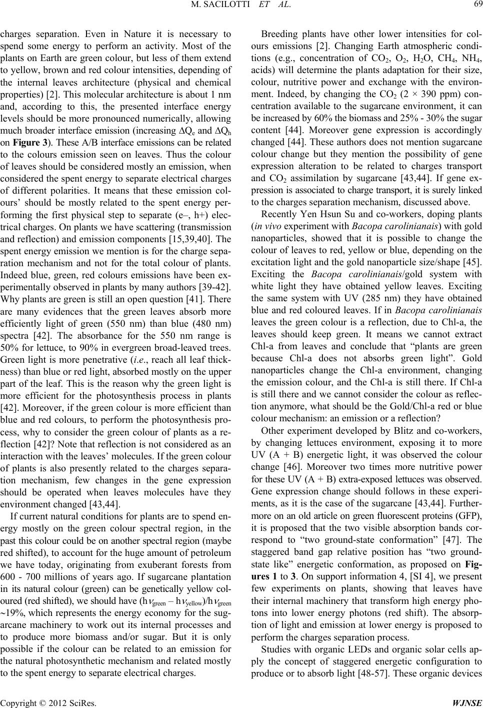 M. SACILOTTI ET AL. 69 charges separation. Even in Nature it is necessary to spend some energy to perform an activity. Most of the plants on Earth are green colour, but less of them extend to yellow, brown and red colour intensities, depending of the internal leaves architecture (physical and chemical properties) [2]. This molecular architecture is about 1 nm and, according to this, the presented interface energy levels should be more pronounced numerically, allowing much broader interface emission (increasing Qe and Qh on Figure 3). These A/B interface emissions can be related to the colours emission seen on leaves. Thus the colour of leaves should be considered mostly an emission, when considered the spent energy to separate electrical charges of different polarities. It means that these emission col- ours’ should be mostly related to the spent energy per- forming the first physical step to separate (e–, h+) elec- trical charges. On plants we have scattering (transmission and reflection) and emission components [15,39,40]. The spent energy emission we mention is for the charge sepa- ration mechanism and not for the total colour of plants. Indeed blue, green, red colours emissions have been ex- perimentally observed in plants by many authors [39-42]. Why plants are green is still an open question [41]. There are many evidences that the green leaves absorb more efficiently light of green (550 nm) than blue (480 nm) spectra [42]. The absorbance for the 550 nm range is 50% for lettuce, to 90% in evergreen broad-leaved trees. Green light is more penetrative (i.e., reach all leaf thick- ness) than blue or red light, absorbed mostly on the upper part of the leaf. This is the reason why the green light is more efficient for the photosynthesis process in plants [42]. Moreover, if the green colour is more efficient than blue and red colours, to perform the photosynthesis pro- cess, why to consider the green colour of plants as a re- flection [42]? Note that reflection is not considered as an interaction with the leaves’ molecules. If the green colour of plants is also presently related to the charges separa- tion mechanism, few changes in the gene expression should be operated when leaves molecules have they environment changed [43,44]. If current natural conditions for plants are to spend en- ergy mostly on the green colour spectral region, in the past this colour could be on another spectral region (maybe red shifted), to account for the huge amount of petroleum we have today, originating from exuberant forests from 600 - 700 millions of years ago. If sugarcane plantation in its natural colour (green) can be genetically yellow col- oured (red shifted), we should have (h green – h yellow)/h green 19%, which represents the energy economy for the sug- arcane machinery to work out its internal processes and to produce more biomass and/or sugar. But it is only possible if the colour can be related to an emission for the natural photosynthetic mechanism and related mostly to the spent energy to separate electrical charges. Breeding plants have other lower intensities for col- ours emissions [2]. Changing Earth atmospheric condi- tions (e.g., concentration of CO2, O2, H2O, CH4, NH4, acids) will determine the plants adaptation for their size, colour, nutritive power and exchange with the environ- ment. Indeed, by changing the CO2 (2 × 390 ppm) con- centration available to the sugarcane environment, it can be increased by 60% the biomass and 25% - 30% the sugar content [44]. Moreover gene expression is accordingly changed [44]. These authors does not mention sugarcane colour change but they mention the possibility of gene expression alteration to be related to charges transport and CO2 assimilation by sugarcane [43,44]. If gene ex- pression is associated to charge transport, it is surely linked to the charges separation mechanism, discussed above. Recently Yen Hsun Su and co-workers, doping plants (in vivo experiment with Bacopa carolinianais) with gold nanoparticles, showed that it is possible to change the colour of leaves to red, yellow or blue, depending on the excitation light and the gold nanoparticle size/shape [45]. Exciting the Bacopa carolinianais/gold system with white light they have obtained yellow leaves. Exciting the same system with UV (285 nm) they have obtained blue and red coloured leaves. If in Bacopa carolinianais leaves the green colour is a reflection, due to Chl-a, the leaves should keep green. It means we cannot extract Chl-a from leaves and conclude that “plants are green because Chl-a does not absorbs green light”. Gold nanoparticles change the Chl-a environment, changing the emission colour, and the Chl-a is still there. If Chl-a is still there and we cannot consider the colour as reflec- tion anymore, what should be the Gold/Chl-a red or blue colour mechanism: an emission or a reflection? Other experiment developed by Blitz and co-workers, by changing lettuces environment, exposing it to more UV (A + B) energetic light, it was observed the colour change [46]. Moreover two times more nutritive power for these UV (A + B) extra-exposed lettuces was observed. Gene expression change should follows in these experi- ments, as it is the case of the sugarcane [43,44]. Further- more on an old article on green fluorescent proteins (GFP), it is proposed that the two visible absorption bands cor- respond to “two ground-state conformation” [47]. The staggered band gap relative position has “two ground- state like” energetic conformation, as proposed on Fig- ures 1 to 3. On support information 4, [SI 4], we present few experiments on plants, showing that leaves have their internal machinery that transform high energy pho- tons into lower energy photons (red shift). The absorp- tion of light and emission at lower energy is proposed to perform the charges separation process. Studies with organic LEDs and organic solar cells ap- ply the concept of staggered energetic configuration to produce or to absorb light [48-57]. These organic devices Copyright © 2012 SciRes. WJNSE  M. SACILOTTI ET AL. 70 are emitting/absorbing light and replacing solid state LED/solar cell, respectively. The organic light emitting/ absorbing are composed of tens of nanosized layers of few tens nanometer thickness. Organic molecules are diluted in a medium and these molecules touch each other at the layers’ interface. A. Heeger (2000 Chemistry Nobel Prize Laureate) used staggered energetic organic/ organic interfaces to produce about 10% efficiency solar cells [52-54]. The energy peak emission at these stag- gered energetic interfaces and layers are broad and in- tense [48-60], a characteristic of type II staggered inter- face energy emission, as represented in Figures 5 and 6 and discussed above. In this paper we discuss the band gap energy emission whenever energetic A/B interfaces are present. As Fluo- rescence Resonance Energy Transfer (FRET) mechanism deals with below band gap emission, we will equally pro- pose few words about the possibility of its explanation be regarded as type II interface emission. Note that FRET model is based on classical physics, described/proposed about 60 years ago by Theodor Forster [13,61]. FRET model suffers from few drawbacks, considering unknown parameters, correction factors, intensities corrections, etc [62,63]. Based on our results, a different model can equally be proposed to explain the “energy transfer” between two different organic or inorganic material pairs, based on the existing and actual band gap energy relative position of both A/B pairs. According to recent experimental works, organic molecules present energetic steps (up or down) for excited electrical charges to travel from a molecule to another one [48,60]. These energetic steps for electrical charges flow, from a molecule to a nearby molecule, are very important and not considered on the FRET theory. These energetic steps can promote energy interface emission (red shifted), observed for many published data explanation. As FRET is a radiationless energy transmis- sion mechanism, we propose that the actual physical/ optical mechanism can be regarded as a radiation inter- face emission mechanism, for many systems, based on type II interface properties. As an example, the applica- tion of the present proposed model can be applied for cyanide dyes (Cy3, Cy5) organic molecules [62,63]. When these molecules pairs are placed together, forming a Cy3/Cy5 interface, an emission peak at 680 nm is ob- served, when excited with 540 nm light [62 and SI-3]. This 680 nm emission of the Cy3/Cy5 system can be associated to type II interface emission. In this way, FRET should deeply be re-discussed as it is based on classical physics and staggered energetic interfaces are based on quantum physics. In this paper, type II interface energetic configuration and interface emission is proposed to explain electrical charges separation. It can equally be proposed to explain many non-comprehensible physical observation like FRET, GFP, green colour of plants and its colours changes by changing the proteins environments [48-60,63]. The me- chanism, based on type II interface, is supported by the quantum mechanical basis, in contrast to the classical the- ory used to explain the photosynthesis first step (charges separation), GFP and FRET. Note that FRET mechanism doe not separate electrical charges. Only the absorption of light is not enough to separate electrons from holes. A question comes about: If FRET is present on the photo- synthesis process, where is it, the charges separation mechanism? Many recent experimental studies propose the photo- synthesis process as quantum mechanics controlled [64- 71]. Forster’s theory is based on classical physics; more- over it is based on a non-existing energetic configuration, as is the case for the GSE representation [4,10,13,15]. Forster theory does not present the necessary electric field to separate electrical charges. It does not present the spent energy to perform this process [13,15]. In summary, the present classical theory violates physical laws, con- cerning the necessary tools to separate electrical charges under attraction. In conclusion to this section, we propose the stag- gered energetic interface (quantum mechanics controlled) to explain the photosynthesis, FRET and GFP processes, instead of the ground state energy (classical physics de- scription) configuration. The staggered configuration has been used between organic molecules to produce organic LEDs and organic solar cells. The staggered configuretion and energy band bending for organics is a real physical property and not a controversial language. It gives us the necessary physical tools to separate electrical charges. If recent optical experiments propose photosynthesis as a quantum mechanics controlled, we should look for quantum physics instead of classical physics. The use of the ground state energetic configuration, to explain the photosynthetic mechanism, is a non-sense physical path- way that should be re-discussed. Under photons excita- tion, charge’s jumping to the nearby organic molecule brings the near interface to a non-equilibrium condition, on both A and B molecules’ electronic structure. The non-equilibrium brings energy band bending (or potential variation) and Fermi level movement (dynamic process). As the A/B generic organic systems are nanometer size and distances, each (e–, h+) wavefunctions should cross few molecules under interaction. It is impossible not to consider this fact on natural systems. Note that the stag- gered energetic configuration can be present at the same organic molecule, as it can be for two different molecules. This molecule can be branched composed, representing an energetic interface of the three types describe above, but never with the GSE configuration. Copyright © 2012 SciRes. WJNSE  M. SACILOTTI ET AL. 71 9. Application of the Charge Separation Mechanism: How to Waste the Visible Light Absorbed Energy by Leaves Electrical charges separation mechanism is not yet well understood for photosynthetic natural and artificial appli- cations. The present preliminary proposition represents a new regard on the photosynthetic natural and artificial electrical charge separation mechanism. Considering it as a new mechanism, most of the parameters necessary to calculate the efficiency (number of separated charges/ number of photons) are not available. According to the present model, it can also be applied to other materials presenting staggered energy configuration, the polymer/ polymer and polymer/inorganic interfaces [49-60]. It can equally occur with the exciton dissociation transferring a single charge to the material A, leaving behind an oppo- site charge in material B [22,34,51]. Excitons from elec- trical charges seated on different materials are different from excitons seated within the same material. The authors are not aware about experimental/theoretical results/ values of excitons when electrical charges of different polarities are seated on different materials or molecules [10,22]. The charge transfer (number of charges/number of photons) for photovoltaics, of about 1% - 6% efficiency, is easily achieved for nanostructured materials [8,10, 16-21]. The same condition is valid for photovoltaic or- ganic/organic or inorganic/inorganic solar cells, in which about 10% efficiency is commonly achieved [10,52-57]. As the material’s properties and its interfaces have an important role, the present model should be applied and improved to increase devices efficiency. Note that the organic/organic interface for LEDs and solar cells uses the staggered energetic configuration, instead of “ground state energy” configuration and that this model cannot be considered as a controversial subject [32-36,49-60]. Concerning the natural photosynthesis, the sunlight energy absorption and the final efficiency by leaves on plants seems to be about 5% [1-3,13]. In this way the application of the present model to estimate the charge separation efficiency needs new experiments, because most of the available data concern non-staggered ener- getic configuration (the GSE one). Moreover the green colour of plants is considered mostly a reflection. It should be emphasised that green leaves have also other minor colours intensity (emission?), such as yellow, brown and red [2]. If these lower intensity colours repre- sent also charges separation within a leaf, caused by a staggered configuration between the energy bands of leaves’ constituents, the efficiency should be verified in consequence. When it occurs, the natural leaves’ consti- tuents should propose many staggered energy configure- tion. Chl and carotene present 3 - 5 main absorption energy peaks [2,13,15]. More efforts are needed to find out the actual energy relative position for each absorption energy band for the leaves’ constituents. To know their energetic relative position, more studies are necessary on the band gap engineering to present the actual energetic configu- ration and both: charges separation and waste of energy to perform the job. Transmittance (T) and reflectance (R) experiments on leaves, within the 400 to 700 nm spectral region, give scattering (S) of about 21% (S = T + R), according to many previous standard experimental results [15,72]. Figure 8 concerns typical reflectance and transmittance curves for leaves, on the visible (400 - 700 nm) and in- fra-red (700 - 1000 nm) spectral regions, showing the necessity for plants to have an efficient way to waste the sun light energy quickly. Maybe the staggered interface is the only appropriate candidate. The absorption expe- riments for isolated Chl-a cannot evidence scientifically that leaves do not absorb on the green region. They rep- resent different systems. Moreover transmittance and reflectance experiments show that leaves reflect on the green colour about 15%, as presented on Figure 8 [15, 72]. The transmittance is about 30% for the 535 nm green spectral region. It means the absorbance is about 55% for the green (535 nm) colour region. 15% for the reflection cannot explain the green colour intensity of plants. Type II interface can be able to absorb and emit nearly the same light wavelength [73]. In this case, the absorption is carried out by an excited electron jumping directly to the nearby material (VB of B material to the CB of A material, Figure 3) [73]. The de-excitation of this electron is followed by the interface emission, emit- ting about the same colour or energy that is absorbed (Figures 2 and 4). Note that interface absorption should create energy band bending on both sides of the A/B in- terface. According to Figure 8, for the visible region (400 - 700 nm), the area below T and R curves gives scattering S = T + R = 21%. As % Absorbance = 100% – (R + T), on average, 79% of the visible spectra is absorbed by leaves, representing a huge amount of energy that plants cannot afford. Nature should invent an efficient way to waste quickly this absorbed sunlight energy. Type II en- ergetic interface can be a good candidate, wasting it as an emission, but related to the spent energy to separate elec- trical charges, a non-efficient quantum mechanism to separate (e–, h+) electrical charges. Maybe nature have got the solution and created type II interface as the mechanism to get ride of most of the 79% average absorption within the 400 - 700 nm solar range (Figure 8) [15,72]. So, if natural photosynthesis effi- ciency is about or below 5% it should be withdraw from 79% absorption, for the 400 - 700 nm visible solar spectra. Artificial photosynthetic nanomaterials get about 1% - 6% Copyright © 2012 SciRes. WJNSE  M. SACILOTTI ET AL. 72 Figure 8. Typical reflectance and transmittance curves for leaves on the visible and infrared spectral regions, evidenc- ing the necessity of an efficient way to waste quickly the sun light energy for plants. Note that there is only 15% of refle- ctance on the green colour region (535 nm). The R + T value at the 400 - 700 nm region gives an average absorbance of about 79%. This is a huge value to be afforded by plants in hot lands. Average values were obtained from the area be- low the R and T curves, for the desired spectral region. R + T is about 98% within the infrared region. There is almost no absorption for the IR region, for plants. The typical R and T results are extracted from references [15,72]. efficiency for their transformation from photons to sepa- rated electrical charges [8,16-20,27-29]. Fig ure 2 and support information 1 [SI-1] show the interface recom- bination/emission is a mechanism to get charges separa- tion [9,12,23-25,30,31]. Moreover, it is not an efficient mechanism to separate electrical charges, because most of the excitation light energy is spent as interface emis- sion. The artificial photosynthetic literature had never touched and related the interface emission as a conse- quence of the low efficiency of the explored devices (1% to 6% efficiency) [8,16-20,27-29]. Here we propose the interface emission mechanism to account for most of these low efficiency natural or artificial devices. In conclusion to this section, according to published data, natural leaves should absorb about 55% of the sun green spectra in the visible region. 15% of reflection does not explain the green “reflection” colour intensity of plants. As leaves absorbs higher photons energy than the green photons and emit lower energy photons (green, yellow, red), to the green colour intensity of leaves it should be added the green transformed by their internal machinery. According to the same published data, leaves should absorb, on average, 79% of the visible sun light spectral region. This enormous quantity has never been discussed in the literature and should be able to cook plants in few min- utes on sunny days. It means that we need a quick and an efficient optical mechanism to get rid of this cooking absorbing system. The same consideration is valid for artificial photosynthetic systems, for which efficiency is low (1% - 6%). Type II energetic interface and its inter- face emission is the only possible configuration to solve the problem: a really efficient way to absorb and waste photons, meanwhile separating few % of the excited (e–, h+) charges. 10. Final Considerations and Conclusions To copy the photosynthetic natural conditions we need to use existing physical conditions that explain the charges separation mechanism. Currently natural photosynthesis mechanism accepted model is not scientifically and phy- sically acceptable: the energetic configuration does not hold on physical basis and neither allows the current physical situation to separate electrical charges with dif- ferent polarities (or charges under attraction). Artificial nanostructured photosynthetic materials models suffer from the same scientific physical drawback: the mecha- nism to separate electrical charges under attraction. In few words, both natural and artificial models violate physical laws if they are not able to present the necessary electric field (the driving force) and the spent energy to separate negative (e–) from positive (h+) charges. Cor- recting these common related drawbacks we can further improve artificial and natural photosynthetic systems and get more energy from the free sunlight source. The solar energy is our only economical pathway if the physical mechanism underling the 2 - 4 billions years of evolution is understood: the charges separation mechanism. If nowadays the solar energy is less efficiently used than in the past (600 - 700 millions of years ago, with a more ele- vated CO2 concentration) for the natural conversion into fuel, we get to a controversial question: is the desertifica- tion a direct consequence of the CO2 atmospheric con- centration decreasing (200 - 370 ppm, years from 1850- 2010) [1-3]? If so, the greenhouse effect should be ob- served differently from current point of view. To this end, the natural and artificial energetic configuration between two different materials should be correctly considered. Excited A/B materials and interfaces can deliver the necessary driving force to separate electrical charges charge (charges with different polarities). The currently defended staggered representation for the II-VI/II-VI and TiO2/II-VI nanosystems, to separate electrical charges, does not present any physical support to separate e– from h+ [16-21,27-29,79-85]. Indeed, these very important experimental results does not explain correctly how elec- trical charges flow as they were gravitational-like balls falling down through stairs [16-21,27-29,73-88]. Unfortu- nately electrical charges should obey electrical parameters. Copyright © 2012 SciRes. WJNSE  M. SACILOTTI ET AL. 73 The misunderstood on electrical charges separation me- chanism has been propagated for many published results [27-29,73-87]. Commonly found assertion like “… the absorption of a photon leads to efficient separation of a single electron-hole pair” is present in the literature, without scientific care [80]. The absorption is only the first step. The subsequent step, to separate (e–, h+), should spend energy. Interface energy band bending has equally been proposed erroneously, even using type II interface to explain electrical charges separation and its flow dire- ction [74,75]. The staggered energy configuration and its band bending should be downwards and not upwards as recently published [74-78]. Basic physical information on electronics and solid-state physics is available every- where and has been constantly neglected [4-7,10,22]. Interface emission has been erroneously attributed to “charge transfer state”, for organic and inorganic systems, meanwhile it is just a recombination of e– with h+ seated on different materials [27-29,51,77,88]. Most of the published data and mechanism explanation uses the flat band configuration to show e– and h+ move- ments across the interface between an A/B generic inter- face [13,15,27-29,48,77-88]. This is proposed for organic and inorganic generic materials [27-29,77-88]. These published work do not consider the energy band bending as exposed above and as exposed in many solid state physics and organic material published data [4-7,9,10,12, 22,36]. The electrical charge jumping from a material to the nearby material creates an electronic non-equilibrium on both materials, moving the quasi-Fermi level (up or down) and, consequently, moving the CB (LUMO) & VB (HOMO) (down or up) [4,10,SI-1]. In summary, it is proposed a model describing the only energetic configuration between two different nano- sized materials, able to provide the necessary electric field to perform (e–, h+) electrical charges separation on photovoltaic systems, such as inorganic/inorganic, inor- ganic/organic and organic/organic interfaces. It is pre- sented, in these descriptions, many systems in which type II interface recombination and emission is the most im- portant electro/optical phenomena: AlInAs/InP, TiO2/II-VI and II-VI/II-VI. These experimental results have been linked to organic solar cells and organic LEDs, in which the staggered energetic configuration is experimentally already known and applied. We have shown that the opti- cally excited AlInAs/InP system has an internal electric field (105 V/cm), issued from the energy band-bending whenever charges jump to the nearby material. The ground state energy (GSE) representation, to explain photosyn- thetic mechanisms, is a non-existing physical energetic configuration. Charges do not care about GSE, charges care about energetic steps if the aim is to separate elec- trons from holes. GSE model does not allow the separa- tion of e– from h+ because it does not promote the basic electric field and the spent energy to separate charges under attraction. Without these two basic physical con- cepts it is impossible to separate (e–, h+) electrical charges in nanosized materials without violating physical laws. Contrary to current believes, charges do not get separated whenever nanomaterials absorb light. This is only the first step and it represents an excitonic attractive entity. The next step, to separate (e–, h+), depends on energetic configurations under which these charges are submitted. Diffusion controlled process on nanometric systems is out of question. Diffusion controlled processes is for the old generation of silicon devices (about 1 m diffusion length). The proposed model, based on stag- gered energetic interfaces and energy band bending, in- troduces equally the concept of spent energy to separate electrical charges. The spent energy is related to the in- terface emission and it can be used to explain most of the photons emission of absorbed visible sunlight (~79%) by plants. It is impossible the surviving of plants without an efficient and quick (optical) way to waste the absorbed visible light. Moreover, the proposed mechanism is quantum controlled, as proposed by many recent experi- mental results on organic molecules. According to pub- lished data, it was shown that, by changing the plants’ environment, there will be change in the biomass and nutritive power. Similarly, by changing the leaves’ mole- cules environment, the leaves’ colour also change. In this way, the colours of plants can be mostly related to the spent energy to separate electrical charges. The green colour being more efficient to promote the photosynthe- sis process, instead of being a reflection, without rela- tionship with the process, can be linked to the charges separation mechanism: it can mostly be linked to the waste, to perform the process and to protect leaves. The ideas and results presented here can be extended to other models or materials/devices as FRET, GFP, CTS, organic LED and organic solar cells. Human needs to know this Nature non-efficient charges separation mechanism to improve its efficiency in natural and in artificial solar energy production. The energetic staggered configuration is an appropriate candidate. But it should be worked out with its intrinsic physical parameters, already described in the literature, but not correctly considered by many photosynthetic workers. If worked out correctly, natural and artificial photosynthetic systems can be adequately copied/improved. Nature obeys physical principals. Men should follow this way, in trying to explain natural and artificial physical mechanisms. Charges separation is a physical and not a biological mechanism. 11. Acknowledgements The authors are grateful to the financial support from ANR-Filemon35-France, and the Fundação de Amparo à Copyright © 2012 SciRes. WJNSE  M. SACILOTTI ET AL. 74 Ciência e Tecnologia do Estado de Pernambuco (FACEPE) and Conselho Nacional de Desenvolvimento Científico e Tecnológico (CNPq) Brazilian agencies. The authors thank professors Cid Araújo, Celso P. Melo, Michael Sundheimer and Dr. Euclides Almeida from DF-UFPE & UFRPE–Brazil and to Dr. Gregory Smestad (from SOL- MAT) for valuables discussions and suggestions. REFERENCES [1] O. Kruse, J. Rupprecht, J. Mussgnug, G. Dismukes and B. Hankamer, “Photosynthesis: A Blueprint for Solar Energy Capture and Biohydrogen Production Technologies,” Pho- tochemical & Photobiological Sciences, Vol. 4, No. 12, 2005, pp. 957-969. doi:10.1039/b506923h [2] H. Peter Raven, F. Ray Evert and S. Eichhorn, “Biologia Vegetal,” 6th Edition, Guanabara Koogan, Rio de Janeiro, 2001, pp. 125, 136, 138, 148. [3] G. C. Dismukes and R. Blankenship, “The Origin and Evolution of Photosynthetic Oxygen Production,” In: B. King, Ed., Encyclopedia of Inorganic Chemistry, 2nd Edi- tion, John Wiley & Sons, Hoboken, 2005, pp. 6696- 6707. [4] H. Kroemer, “Nobel Lecture: Quasielectric Fields and Band Offsets: Teaching Electrons New Tricks,” Reviews of Modern Physics, Vol. 73, No. 3, 2001, pp. 783-793. doi:10.1103/RevModPhys.73.783 [5] H. Kroemer, “Staggered-Lineup Heterojunctions as Sources of Tunable Below-Gap Radiation: Operating Principle and Semiconductor Selection,” IEEE Electron Device Letters, Vol. 4, No. 1, 1983, pp. 20-22. [6] L. Esaki, “A Bird’s-Eye View on the Evolution of Semi- conductors Superlattices and Quantum Wells,” IEEE Quantum Electronics, Vol. 22, No. 9, 1986, pp. 1611- 1624. doi:10.1109/JQE.1986.1073162 [7] H. Kroemer, “Barrier Control and Measurements: Abrupt Semiconductor Heterojunctions,” Journal of Vacuum Sci- ence & Technology B, Vol. 2, No. 3, 1984, pp. 433-439. [8] M. Gratzel, “Photoelectrochemical Cells,” Nature, Vol. 414, No. 15, 2001, pp. 338-344. doi:10.1038/35104607 [9] M. Sacilotti, P. Abraham, M. Pitaval, M. Ambri, T. Ben- yattou, A. Tabata, M. Perez, P. Motisuke, R. Landers, A. Lecore and S. Loualiche, “Structural and Optical Proper- ties of AlInAs/InP and GaPSb/InP Type II Interfaces,” Canadian Journal of Physics, Vol. 74, No. 5-6, 1996, pp. 202-208. doi:10.1139/p96-032 [10] M. S. Sze, “Physics of Semiconductor Devices,” 1st Edi- tion, John Wiley & Sons Inc., Chichester, 1969, pp. 32-38, & 3rd Edition, 2007, pp. 27, 58, 79, 104, 123, 128, 134, 457, 601, 663. [11] F. De Angelis, S. Fantacci and A. Selloni, “Alignment of the Dye’s Molecular Levels with the TiO2 Band Edges in Dye-Sensitized Solar Cells: A Dft-Tddft Study,” Nanotech- nology, Vol. 19, No. 42, 2008, Article ID: 424002-09. doi:10.1088/0957-4484/19/42/424002 [12] M. Sacilotti, E. Almeida, C. B. Mota, F. D. Nunes, Th. Vasconcelos and M. Sundheimer, “A Proposed Quantum Mechanics Mechanism for (e–, h+) Charges Separation Applied to Photosynthesis and Energy Production Effi- ciency Improovement,” Optical Society of America, Fron- tiers in Optics, San Jose, 11 October 2009. http://www.opticsinfobase.org/viewmedia.cfm?uri=FiO-2 009-PDPC5&seq=0 [13] J. R. Bolton, “Solar Power and Fuels,” Academic Press Inc., New York, 1977, p. 229. [14] V. Sundstrm, T. Pullerits and R. Grondelle, “Photosynthetic Light-Harvesting: Reconciling Dynamics and Structure of Purple Bacterial LH2 Reveals Function of Photosynthetic Unit,” The Journal of Physical Chemistry B, Vol. 103, No. 13, 1999, pp. 2327-2346. doi:10.1021/jp983722+ [15] L. O. Bjorn, G. Papageorgiou, R. Blankenshi and K. Go- vindjee, “A View Point: Why Chlorophylla?” Photosyn- thesis Research, Vol. 99, No. 2, 2009, pp. 85-98. [16] L. Wei, C. Liu, Y. Zhou, Y. Bai, X. Feng, Z. Yang, L. Lu, X. Lu and K. Chan, “Enhanced Photovoltaic Activity in Anatase/TiO2(B) Core-Shell Nanofiber,” The Journal of Physical Chemistry C, Vol. 112, No. 51, 2008, pp. 20539- 20545. [17] S. S. Srinivasan, J. Wade and E. Stefanakos, “Visible Light Photocatalysis via CdS/TiO2 Nanocomposite Materi- als,” Journal of Nanomaterials, Vol. 2006, 2006, pp. 1-7, Article ID: 87326. doi:10.1155/JNM/2006/87326 [18] I. Robel, V. Subramanian, M. Kuno and P. Kamat, “Quantum Dot Solar Cells. Harvesting Light Energy with CdSe Nanocrystals Molecularly Linked to Mesoscopic TiO2 Films,” Journal of the American Chemical Society, Vol. 128, No. 7, 2006, pp. 2385-2393. doi:10.1021/ja056494n [19] P. V. Kamat, “Quantum Dot Solar Cells. Semiconductor Nanocrystals as Light Harvesters,” The Journal of Physical Chemistry C, Vol. 112, No. 48, 2009, pp. 18737-18753. [20] D. Robert, “Photosensitization of TiO2 by MxSy and MxSy Nanoparticles for Heterogeneous Photocatalysis Applica- tions,” Catalysis Today, Vol. 122, No. 1-2, 2007, pp. 20-26. doi:10.1016/j.cattod.2007.01.060 [21] J. Zhang, H. Zhu, S. Zheng, F. Pan and T. Wang, “TiO2 Film/Cu2O Microgrid Heterojunction with Photocatalytic Activity under Solar Light Irradiation,” Applied Materials & Interfaces, Vol. 1, No. 10, 2009, pp. 2111-2114. doi:10.1021/am900463g [22] M. Fox, “Optical Properties of Solids. Oxford Master Series in Condensed Matter Physics,” Oxford University Press, Oxford, 2001, pp. 76-78. [23] P. Abraham, M. Perez, T. Benyattou, G. Guillot, M. Sacilotti and X. Letartre, “Photoluminescence and Band Offsets of AlInAs/InP,” Semiconductor Science and Tech- nology, Vol. 10, No. 12, 1995, pp. 1585-1595. doi:10.1088/0268-1242/10/12/006 [24] M. Sacilotti, P. Motisuke, Y. Monteil, P. Abraham, F. Iikawa, C. Montes, M. Furtado, L. Horiuchi, R. Landers, J. Morais, L. Cardoso, J. Decobert and B. Waldman, “Growth and Characterization of Type-II/Type-I AlGaInAs/InP In- terfaces,” Journal of Crystal Growth, Vol. 124, No. 1-4, 1992, pp. 589-595. doi:10.1016/0022-0248(92)90522-K [25] R. Sakamoto, T. Kohnot, T. Kamiyoshi, M. Inoue, S. Copyright © 2012 SciRes. WJNSE  M. SACILOTTI ET AL. 75 Nakajima and H. Hayashi, “Optical Analysis of Hot Car- rier Distribution and Transport Properties in InP/AlInAs Type II Heterostructures,” Semiconductor Science and Tech- nology, Vol. 7, No. 3B, 1992, pp. B271-B273. doi:10.1088/0268-1242/7/3B/066 [26] A. Selloni, “Anatase Shows Its Reactive Side,” Nature Materials, Vol. 7, 2008, pp. 613-615. doi:10.1038/nmat2241 [27] S. Kumar, M. Jones, S. Lo and G. Scholes, “Nanorod Heterostructures Showing Photoinduced Charge Separa- tion,” Small, Vol. 3, No. 9, 2007, pp. 1633-1639. doi:10.1002/smll.200700155 [28] G. Scholes, “Controlling the Optical Properties of Inor- ganic Nanoparticles,” Advanced Functional Materials, Vol. 18, No. 8, 2008, pp. 1157-1172. doi:10.1002/adfm.200800151 [29] S. Kumar and G. Scholes, “Colloidal Nanocrystal Solar Cells,” Microchim Acta, Vol. 160, No. 3, 2008, pp. 315- 325. doi:10.1007/s00604-007-0806-z [30] M. Sacilotti, E. Almeida, C. Mota, F. D. Nunes and A. S. L. Gomes, “Can the Photosynthesis First Step Quantum Mechanism Be Explained?” http://arxiv.org/abs/1005.1337 [31] M. Sacilotti, E. Almeida, C. Mota, Th. Vasconcelos, F. D. Nunes and A. S. L. Gomes, “A New Quantum Optical Structure to Separate Attracting Electrical Charges,” The Latin America Optics and Photonics Conference, Vol. 1, 2010, pp. 1-4. http://www.opticsinfobase.org/abstract.cfm?uri=LAOP-2 010-TuA3 [32] S. Yin and T. Sato, “Synthesis and Photocatalytic Proper- ties of Fibrous Titania Prepared from Protonic Layered Tetratitanate Precursor in Supercritical Alcohols,” Indus- trial & Engineering Chemistry Research, Vol. 39, No. 12, 2000, pp. 4526-4530. doi:10.1021/ie000165g [33] M. R. Hoffmann, S. T. Martin, W. Choi and D. W. Bah- nemannt, “Environmental Applications of Semiconductor Photocatalysis,” Chemical Reviews, Vol. 95, No. 1, 1995, pp. 69-96. doi:10.1021/cr00033a004 [34] A. Fujishima and K. Honda, “Electrochemical Photolysis of Water at a Semiconductor Electrode,” Nature, Vol. 238, No. 7, 1972, pp. 37-38. doi:10.1038/238037a0 [35] J.-L. Brédas, “Molecular Understanding of Organic Solar Cells: The Challenges,” Accounts of Chemical Research, Vol. 42, No. 11, 2009, pp. 1691-1699. doi:10.1021/ar900099h [36] H. Ishii, K. Sugiyama, E. Ito and K. Seki, “Energy Level Alignment and Interfacial Electronic Structures at Or- ganic/Metal and Organic/Organic Interfaces,” Advanced Materials, Vol. 11, No. 8, 1999, pp. 605-625. doi:10.1002/(SICI)1521-4095(199906)11:8<605::AID-A DMA605>3.0.CO;2-Q [37] T.-C. Tseng, Ch. Urban, Y. Wang, R. Otero, S. Tait, M. Alcami, D. Ecija, M. Trelka, J. M. Gallego, N. Lin, M. Konuma, U. Starke, A. Nefedov, A. Langner, Ch. Woll, M. Herranz, F. Martin, K. Kern and R. Miranda, “Charge-Transfer-Induced Structural Rearrangements at Both Sides of Organic/Metal Interfaces,” Nature Chemis- try, Vol. 2, 2010, pp. 374-379. doi:10.1038/nchem.591 [38] C. Santato and F. Rosei, “Seeing Both Sides,” Nature Chemistry, Vol. 2, No. 5, 2010, pp. 344-345. doi:10.1038/nchem.636 [39] M. Broglia, “Blue-Green Laser-Induced Fluorescence from Intact Leaves: Actinic Light Sensitivity and Subcel- lular Origins,” Applied Optics, Vol. 32, No. 3, 1993, pp. 334-338. doi:10.1364/AO.32.000334 [40] E. Chappelle, F. Wood, W. Newcomb and J. Mcmurtrey, “Laser-Induced Fluorescence of Green Plants. LIF Spec- tral Signatures of Five Major Plant Types,” Applied Op- tics, Vol. 24, No. 1, 1985, pp. 74-80. doi:10.1364/AO.24.000074 [41] T. Gillbro and R. Cogdell, “Carotenoid Fluorescence,” Chemical Physics Letters, Vol. 158, No. 3-4, 1989, pp. 312-316. doi:10.1016/0009-2614(89)87342-7 [42] I. Terashima, T. Fujita, T. Inoue, W. Chow and R. Oguchi, “Green Light Drives Leaf Photosynthesis More Effi- ciently than Red Light in Strong White Light: Revisiting the Enigmatic Question of Why Leaves Are Green,” Plant & Cell Physiology, Vol. 50, No. 4, 2009, pp. 684-697. doi:10.1093/pcp/pcp034 [43] A. P. de Souza, M. Gaspar, E. A. da Silva, E. C. Ulian, A. J. Waclawovsky, M. Y. Nishiyama Jr., R. V. D. Santos, M. M. Teixeira, G. M. Souza and M. S. Buckeridge, “Elevated CO2 Increases Photosynthesis, Biomass and Productivity, and Modifies Gene Expression in Sugar- cane,” Plant, Cell & Environment, Vol. 31, No. 8, 2008, pp. 1116-1127. doi:10.1111/j.1365-3040.2008.01822.x [44] A. P. de Souza and M. S. Buckeridge, “Photosynthesis in Sugarcane and Its Strategic Importance to Face the Global Climatic Change,” In: LAB Cortez, Ed., Sugarcane Bio- ethanol: R & D for Productivity and Sustainability, Ed- gard Blucher, São Paulo, 2010, pp. 320-323. [45] Y. H. Su, S. L. Tu, S. W. Tseng, Y. C. Chang, S. H. Chang and W. M. Zhang, “Influence of Surface Plasmon Resonance on the Emission Intermittency of Photolumi- nescence from Gold Nano-Sea-Urchins,” Nanoscale, Vol. 2, No. 12, 2010, pp. 2639-2646. doi:10.1039/c0nr00330a [46] S. Blitz, “Lettuce Carotenoids Affected by UV Light in Greenhouse,” 2009. http://www.ars.usda.gov/is/np/Fnrb/fnrb0409.htm#lettuce [47] M. Chattoraj, B. A. King, G. U. Bublitz and S. G. Boxer, “Ultra-Fast Excited State Dynamics in Green Fluorescent Protein: Multiple States and Proton Transfer,” Proceed- ings of the National Academy of Sciences of the United States of America, Vol. 93, No. 16, 1996, pp. 8362-8367. doi:10.1073/pnas.93.16.8362 [48] Q. Xiangfei, M. Slootsky and S. Forrest, “Stacked White Organic Light Emitting Devices Consisting of Separate Red, Green, and Blues Elements,” Applied Physics Let- ters, Vol. 93, No. 19, 2008, pp. 193306-193313. doi:10.1063/1.3021014 [49] Y. Sun and S. Forrest, “High-Efficiency White Organic Light Emitting Devices with Three Separate Phosphores- cent Emission Layers,” Applied Physics Letters, Vol. 91, No. 26, 2007, Article ID: 263503-26356. doi:10.1063/1.2827178 Copyright © 2012 SciRes. WJNSE  M. SACILOTTI ET AL. 76 [50] L. Koster, E. Smits, V. Mihailetchi and P. Blom, “Device Model for the Operation of Polymer/Fullerene Bulk Het- erojunctions Solar Cells,” Physical Review B, Vol. 72, No. 8, 2005, Article ID: 085205-085214. doi:10.1103/PhysRevB.72.085205 [51] J. J. Hall, J. Cornil, D. Santos, R. Silbey, D. Hwang, A. Holmes, J.-L. Brédas and R. Friend, “Charge and Energy Transfer Processes at Polymer/Polymer Interfaces: A Joint Experimental and Theoretical Study,” Physical Re- view B, Vol. 60, No. 8, 1999, pp. 5721-5727. doi:10.1103/PhysRevB.60.5721 [52] C. Soci, I. Hwang, D. Moses, Z. Zhu, D. Walter, R. Gaudiana, C. Bradec and A. Heeger, “Photoconductivity of a Low-Bandgap Conjugated Polymer,” Advanced Func- tional Materials, Vol. 17, No. 4, 2007, pp. 632-636. doi:10.1002/adfm.200600199 [53] X. Gong, M. Robinson, J. Ostrowski, D. Moses, G. Bazan and A. J. Heeger, “High-Efficiency Polymer-Based Elec- trophosphorescent Devices,” Advanced Materials, Vol. 14, No. 8, 2002, pp. 581-585. doi:10.1002/1521-4095(20020418)14:8<581::AID-ADM A581>3.0.CO;2-B [54] K. Lee and A. J. Heeger, “Optical Investigation of Intra and Interchain Charge Dynamics in Conducting Polymers,” Synthetic Metals, Vol. 128, No. 3, 2002, pp. 279-282. doi:10.1016/S0379-6779(02)00006-1 [55] M. Koppe, M. Scharber, C. Brabec, W. Duffy, M. Heeney and I. McCulloch, “Polyterthiophenes as Donors for Polymer Solar Cells,” Advanced Functional Materials, Vol. 17, No. 8, 2007, pp. 1371-1376. doi:10.1002/adfm.200600859 [56] A. J. Heeger, “The Plastic-Electronics Revolution,” In- formation Display, Vol. 18, No. 2, 2002, pp. 18-20. [57] K. Coakley and M. McGehee, “Conjugated Polymer Photo- voltaic Cells,” Chemistry of Materials, Vol. 16, No. 23, 2004, pp. 4533-4542. doi:10.1021/cm049654n [58] J. Szollosi, S. Damjanovich and L. Matyus, “Application of Fluorescence Energy Transfer in the Clinical Laboratory: Routine and Research,” Cytometry, Vol. 34, No. 4, 1998, pp. 159-179. doi:10.1002/(SICI)1097-0320(19980815)34:4<159::AID- CYTO1>3.0.CO;2-B [59] S. Weiss, “Fluorescence Spectroscopy of Single Biomole- cules,” Science, Vol. 283, No. 5408, 1999, pp. 1676-1683. doi:10.1126/science.283.5408.1676 [60] A. Kahn, W. Zhao, W. Gao, H. Vazquez and F. Flores, “Doping-Induced Realignment of Molecular Levels at Or- ganic-Organic Heterojunctions,” Chemical Physics, Vol. 325, No. 1, 2006, pp. 129-137. [61] Th. Förster, “Intermolecular Energy Migration and Fluores- cence,” Ann Physik, Vol. 2, No. 1-2, 1948, pp. 55-75. [62] P. Held, “An Introduction to Fluorescence Resonance Energy Transfer Technology and Its Application in Bio- science,” Bio Tek. http://www.biotek.com/resources/docs/Fluorescence_Res onance_Energy_Transfer_Technology_FRET_App_Note. pdf [63] P. L. Southwick, L. A. Ernst, E. W. Tauriello, S. R. Parker, R. B. Mujumdar, S. R. Mujumdar, H. A. Clever, and A. S. Waggoner, “Cyanine Dye Labeling Reagents— Car- boxymethylindocyanine Succinimidyl Esters,” Cytome- try, Vol. 11, No. 3, 1990, pp. 418-430. doi:10.1002/cyto.990110313 [64] J. Herek, W. Wohlleben, R. Cogdell, D. Zeidler and M. Motzkus, “Quantum Control of Energy Flow in Light Harvesting,” Nature, Vol. 417, 2002, pp. 533-535. [65] G. Fleming and G. Scholes, “Quantum Mechanics for Plants,” Nature, Vol. 431, 2004, pp. 256-257. [66] T. Brixner, J. Stenger, H. Vaswani, M. Cho, R. Blankenship and G. Fleming, “Two-Dimensional Spectroscopy of Elec- tronic Coupling in Photosynthesis,” Nature, Vol. 434, 2005, pp. 625-628. [67] R. Sension, “Quantum Path to Photosyntesis,” Nature, Vol. 446, 2007, pp. 740-741. [68] G. Engel, T. Calhoun, E. Read, T. Ahn, T. Mançal, Y. Cheng, R. Blankenship and G. Fleming, “Evidence for Wavelike Energy Transfer through Quantum Coherence in Photosynthetic Systems,” Nature, Vol. 446, 2007, pp. 782-786. [69] G. Engel and G. Fleming, “Quantum Secrets of Photo- synthesis Revealed,” 2007. File://Users/sacilotti/Desktop/ToutFotosintese:Catalise:W OLED/PhotosynthesisQuantum/Quantum%20secrets%20 of%20photosynthesis%20revealed.webarchive [70] M. Schirber, “The Quantum Dimension of Photosynthe- sis,” 2009. http://focus.aps.org/story/v23/st5#author [71] I. Mercer, Y. E. Kajumba, J. Marangos, J. Tisch, M. Gab- rielsen, R. Cogdell, E. Springate and E. Turcu, “Instanta- neous Mapping of Coherently Coupled Electronic Transi- tions and Energy Transfers in a Photosynthetic Complex Using Angle-Resolved Coherent Optical Wave-Mixing,” Physical Review Letters, Vol. 102, No. 5, 2009, Article ID: 057402-4. doi:10.1103/PhysRevLett.102.057402 [72] S. Seager, E. Turner, J. Schafer and E. Ford, “Vegeta- tion’s Red Edge: A Possible Spectroscopic Biosignature of Extraterrestrial Plants,” 2005. http://Arxiv:astro-phy/0503302v1 [73] P. Pearson, R. Bergstrn and S. Lunell, “Quantum Chemi- cal Study of Photoinjection in Dye-Sensitized TiO2 Nanopati- cles,” The Journal of Physical Chemistry B, Vol. 104, No. 44, 2000, pp. 10349-10351. [74] J. Sambur, Th. Novet and B. Parkinson, “Multiple Exci- ton Collection in a Sensitized Photovoltaic System,” Sci- ence, Vol. 330, No. 6000, 2010, pp. 63-66. doi:10.1126/science.1191462 [75] Z. Yang, T. Xu, Y. Ito, U. Welp and W. Kwok, “En- hanced Electron Transport in Dye-Sensitized Solar Cells Using Short ZnO Nanotips on a Rough Metal Anode,” The Journal of Physical Chemistry C, Vol. 113, No. 47, 2009, pp. 20521-20526. doi:10.1021/jp908678x [76] J. Chen, W. Lei and W. Deng, “Reduced Charge Recom- bination in a Co-Sensitized Quantum Solar Cell with Two Different Sizes of CdSe Quantum Dot,” Nanoscale, Vol. 3, No. 2, pp. 674-677. doi:10.1039/C0NR0059IF [77] T. M. Clarke and J. R. Durrant, “Charge Photogeneration in Organic Solar Cells,” Chemical Reviews, Vol. 110, No. Copyright © 2012 SciRes. WJNSE  M. SACILOTTI ET AL. Copyright © 2012 SciRes. WJNSE 77 11, 2010, pp. 6736-6767. doi:10.1021/cr900271s [78] R. H. Friend, M. Phillips, A. Rao, M. Wilson, Z. Li and Ch. MacNeil, “Excitons and Charges at Organic Semicon- ductor Heterojunctions,” Faraday Discussion, Vol. 155, No. 1-10, 2012, pp. 339-348. [79] J. Servaites, M. Ratner and T. Marks, “Organic Solar Cells: A New Look at Traditional Models,” Energy & Environmental Science, Vol. 4, No. 11, 2011, pp. 4410- 4422. [80] L. Hammarstrom and S. Styring, “Proton-Coupled Elec- tron Transfer of Tyrosines in Photosystem II and Model Systems for Artificial Photosynthesis: The Role of a Re- dox-Active Link between Catalyst and Photosensitiser,” En- ergy & Environmental Science, Vol. 4, No. 7, 2011, pp. 2379-2388. [81] Ch. Herrero, A. Quaranta, W. Leibl, A. W. Rutherford and A. Aukauloo, “Artificial Photosynthetic Systems,” Energy & Environmental Science, Vol. 4, No. 7, 2011, pp. 2353-2365. [82] P. Marek, H. Hahn and T. Balaban, “On the Way to Biomimetic Dye Aggregate Solar Cells,” Energy & En- vironmental Science, Vol. 4, No. 7, 2011, pp. 2366-2378. [83] Th. Woolerton, S. Sheard, E. Pierce, S. Rasdale and F. Arm- strong, “CO2 Photoreduction at Enzyme-Modified Metal Oxide Nanoparticles,” Energy & Environmental Science, Vol. 4, No. 7, 2011, pp. 2393-2399. [84] P. Poddutoori, D. Co, A. Samuel, C. Kim, T. Vagnini and M. Wasielewski, “Photoiniciated Multistep Charge Sepa- ration in Ferrocene-Zinc Porphyrin-Diiron Hydrogenase Model Complex Triads,” Energy & Environmental Sci- ence, Vol. 4, No. 7, 2011, pp. 2441-2450. [85] K. Shimura and H. Yoshida, “Heterogeneuous Photocata- lytic Hydrogen Production from Water and Biomass De- rivatives,” Energy & Environmental Science, Vol. 4, No. 7, 2011, pp. 2467-2481. [86] M. Freitag and E. Galoppini, “Molecular Host-Guest Com- plexes: Shielding of Guests on Semiconductor Surfaces,” Energy & Environmental Science, Vol. 4, No. 7, 2011, pp. 2482-2494. [87] A. Cannavale, M. Manca, F. Malara, L. de Marco, R. Cin- golani and G. Gigli, “Highly Efficient Smart Photovolta- chromic Devices with Tailored Electrolyte Composi- tion,” Energy & Environmental Science, Vol. 4, No. 7, 2011, pp. 2567-2574. [88] A. A. Bakulin, A. Rao, V. G. Pavelyev, P. H. M. van Loos- drecht, M. S. Pshenichnikov, D. Niedzialek, J. Cornil, D. Beljonne and R. H. Friend, “The Role of Driving Energy and Delocalized States for Charge Separation in Organic Semiconductors,” Science, Vol. 335, No. 6074, 2012, pp. 1340-1344. http://www-oe.phy.cam.ac.uk/oepubs/oepubsummary.htm doi:10.1126/science.1217745.  M. SACILOTTI ET AL. 78 Support Information SI-1. Energy Staggered Interface: Electrical Charge Separation Mechanism Résumé The following slides present how the proposed mech- anism does work, based on the excitation of one hypo- thetical interface between (Material A)/(Material B). This excitation is performed with only 4 photons. It is, equally, represented why the interface recombination/ emission process has a so large emission peak. The (e–, h+) wavefunctions penetration is represented for the AlInAs/InP system. The present SI-1 should be viewed in a ppt version by clicking below. Figure SI-1-1 repre- sents energy band bending mechanism. Figure SI-1-2 represents the jumping of charges to the nearby material. Figure SI-1-3 represents the separated charges and its catalytic action. Figure SI-1-4 represents the two quasi- triangular quantum wells at the interface, to explain the interface emission peak broadness. Figure SI-1-5 repre- sents the two quasi-triangular quantum wells at the in- terface, to explain the e– h+ wavefunctions overlap. Comments The natural photosynthetic first step process is based on the light absorption and followed by electrical charges separation on leaves. Only the absorption of light does not separate e– from h+. The absorption of light creates (e–, h+) pairs. For the separation we need an appropri- ated energetic configuration. The present existing Forster’s model, to explain the photosynthetic first step process, is based on classical physics. The same ideas are applied to artificial systems. The present accepted model violates mainly three physi- cal laws. 1) The energetic configuration, that represents the en- ergy transfer from a molecule A to a nearby molecule B, does not exist in physics (the ground state energy repre- sentation). Charges do not care about the ground state energy configuration. Charges care about energetic steps (up or down). 2) To separate negative from positive charges, the necessary electric field is not present. The absorption of light does not separate electrical charges. This is just the first step of the process. To do the next part we need an appropriate energetic configuration that allows the appa- rition of the electric field. This electric field must come from a varying potential. 3) To separate electrical charges under attraction we must spend energy. Note that the excitonic attraction energy between e– and h+ on organic molecules is about 10 to 50 times that ones present on inorganic materials. This means that we need a much stronger electric field for organics, to separate (e–, h+). Moreover, recent papers (about 10), published in Nature, Science, PRL, (see text), show evidences that the photosynthesis first step mecha- nism is quantum mechanics controlled. The enclosed and proposed mechanism does not suffer from these drawbacks (1 to 3). It is a photonic quantum mechanics mechanism. Click here to see the ppt slow motion model. Note: the ppt pictures were prepared in a Machintosh computer. Version: SI-2. Mathematics Calculus (Wavefunction, Probabilities Densities) Résumé The following pages present details of the calculations Figure SI-1-1. Representing the energy staggered interface: electrical charge separation mechanism. How does the energy band bending arrive at the energetic interface? The flow of charges from one material to the nearby material creates an elec- tronic no-equilibrium on both materials, near the interface. This electronic non-equilibrium creates potential variation. It creates the necessary electric field to separate charges: e– from h+. Copyright © 2012 SciRes. WJNSE  M. SACILOTTI ET AL. 79 Figure SI-1-2. Representing the energy staggered interface. It represents the charge separation mechanism in a picturial slow motion maner. Excitation of such an energetic structure with only 4 photons. Figure SI-1-3. Representing the energy staggered interface: charge separation mechanism applied to photosynthetic first step processes. Note the hudge electric field crossing the interface for the AlInAs/InP system (see text). For organic molecules, this electric field should be much higher since the excitonic attraction is much higher than for inorganic materials. Why is the interface emission peak so large? See it in the nexts slides… Figure SI-1-4. Representing the interface physical parts linked to the interface emission peak. All the terms of the equation below should change with the excitation intensity. Mainly ∆Qe + ∆Qh should change more than the others terms. This explain why the interface PL & EL emission peaks’ are so large. Copyright © 2012 SciRes. WJNSE  M. SACILOTTI ET AL. Copyright © 2012 SciRes. WJNSE 80 Figure SI-1-5. Representing the interface physical parts linked to the interface recombination/emission peak. The interface recombination and emission depends on the e− & h+ wavefunctions’ interface overlap. The 1 to 2 nm wave-function penetration is for the AlInAs/InP system (see text). for the probability density and the (e–, h+) wavefunction overlap at the AlInAs/InP interface. In this work the bands are modelled as exponential bended bands, leading to Bessel wavefunctions for carriers. Energy levels of car- riers at valence and conduction bands, as well tunnelling length, for each kind of carrier are calculated by solving the transcendental equation obtained for wave function continuity at the interface. Parameters for the present calculation were taken from reference. Abraham, P. et al. Photoluminescence and band offsets of AlInAs/InP. Semiconductor Sci. Technology 10, 1-10 (1995) [23]. Comments The photon excited staggered AlInAs/InP interface gives rise to an interface electric field of about 105 V/cm. This is approximately the same value obtained for the ex- perimental result of Figure SI-2-1 (see text). The calcu- lated e– wavefunction penetration on the AlInAs material is about 2 nm. The calculated h+ wavefunction on the InP material is about 1 nm. Both values account for the interface (e–, h+) recombination and interface intense emission. Figure SI-2-1. The scheme of tilted electronic bands for AlInAs/InP. These equations are applied to both the calculation of energy levels for the holes in the valence band and for the electrons in the conduction band. In each case we should observe the proper values of the parameters of the Table 1. Using the transformation of variables Both bands of valence and conduction bands have similar, bent on account of them injected carriers. In each of the potential will be approximated by exponential functions as shown in Equation (1) and picture in Figure SI-2-1. /2 2 /2 2 2 2 2 2Δ xσ xη m ξσ δe m ξη e (3) / / 1 1 Δ1 xσ o xη VxV δex Vx Vex 0 0 (1) Substituting these potentials in the Schroedinger equa- tion we have: We get the following equations: 2 222 2 2 222 2 dd 40 0 d d dd 40 0 d d ψψ ξξξνψx ξ ξ ψψ ξξξμψx ξ ξ (4) 2 / 22 2 / 1 22 d2 1 0 d d2 Δ 1 0 d xσ o xη ψmEVδeψx x ψmEVe ψx 0 0 (2)  M. SACILOTTI ET AL. 81 These are the known Bessel equations in which it is defined the parameters: 2 2 2 2 2 1 2 2 2 o mVE mVE (5) The solutions for the Equations (4) will be: 2 2 AJ 0 BI 0 xx xx (6) These solutions must satisfy the boundary conditions at x = 0. Equating the functions and their derivatives at x = 0 results the transcendental equation: 21 21 22 I2 J2 J2 I2 u v vu vvv u (7) The probability density is represented by 2 P x (8) The parameters concerning the potential wells in the conduction band and valence are those given in Table 1. Solving the transcendental equations for the valence and conduction bands it was obtained two energy levels for holes (VB) and one energy level for electrons (CB) in the conduction band. The energies and the parameters that determine the wave functions for electrons and holes are given in Table 2 and the density probabilities are represented in Figures SI-2-2 and SI-2-3. SI-3. Fluorescence Resonance Energy Transfer (FRET), Presented as Type II Interface Emission Résumé The following pages present how the proposed mecha- Table 1. Parameters for the potential wells. Vo (meV) V1 (meV) (meV) (meV) (nm) (nm) me 0 349 60 20 5 5 0.07 0 272 60 20 5 5 0.4 Table 2. Energies and parameters determining the wave functions for electrons and roles. A B E (meV) V1-E(meV) Electrons 0.491 804.794 54.68 5.32 1.223 5.313 × 10538.85 232.68 Holes 0.689 −9.9 × 10⁴ 56.13 215.87 nism does work for FRET. Fluorescence resonance en- ergy transfer (FRET), is a physical phenomenon by means of which electronic excitation can pass from one chemical unit to another, following the absorption of light. The chemical unit we are discussing here is only for chromophores. In this support information, FRET is observed as a type II interface emission and not as an energy transfer from one material to the nearby material. It is presented just one example for organic cyanine dyes molecules. The same idea can also be applied to green P(x) X (nm) -5 0 5 10 20 -10 -20 0 0.125 0.250 Holes Electrons AlInAs/InP interface Holes _ _ Figure SI-2-2. It shows the probability density versus dis- tance within the structure, for the valence band and con- duction band, where we see that the penetration probability for electrons and holes beyond the wall of the well. The region with interpenetrating wavefunctions is pointed out in the figure by pink colored rectangle. Band gap energy -20-12-4 0 4 122 X (nm) -200 -100 0 0 100 200 300 Conduction Band electrons Valence Band holes AlInAs InP P(x) meV meV P(x) Figure SI-2-3. It shows schematically, with the values of the energy-scale the probability densities for electrons and holes relative to the potential wells within the system AlInAs/InP. X (nm) is the distance from the interface. Copyright © 2012 SciRes. WJNSE  M. SACILOTTI ET AL. 82 fluorescent proteins (GFP) as well. These ideas are pre- sented on Figures SI-3-1, SI-3-2 and SI-3-3. They have the explanation text for each one figure. SI-4. Experiments with Leaves Résumé The following pages present how the proposed mecha- nism does work for leaves from plants. This SI presents experiments with leaves, showing their internal trans- formation machine, absorbing higher energy photons and × × Figure SI-3-1. Representation of an A/B type II generic interface, showing the motion for the energy band bending and the quasi-Fermi levels displacements, whenever the A/B system is excited by photons which energy is higher than both A & B materials’ band gap. At the interface, the energy staggered interface (type II): electrical charge sepa- ration mechanism, by an existing interface electric field. This electric field comes from a varying potential, which origin is from the energy band bending at the interface. Whenever charges jump to the nearby material, the elec- tronic environment is changed in both materials. This change creates the potential variation and the interface electric field. This interface and its properties are applied to explain FRET. Figure SI-3-2. Intensity (I) versus wavelength ( ) for optical properties of cyanides molecules. Representation of the absorption (A) and emission (E) regions for Cy3 & Cy5 organic cyanine dyes [62,63]. The dashed common region represents the overlap between the Cy3 emission region and the Cy5 absorption region of these molecules. Following FRET mechanism, the common A & E region for both molecules allows the Cy3 molecule be excited on the 525 - 550 nm region and the Cy5 molecule to emit within the 670 - 700 nm region. This red-shifted emission is proposed to be type II interface related in the next Figure SI-3-3. emitting lower energy photons. Leaves are considered to have about 1 nm size proteins, separated by about 1 nm distance. These dimensions give about 1020 energetic interfaces/cm3. This is above the doping density (1017 to 1018 atoms/cm3) for inorganic semiconductor optical de- vices or organic optical devices. These numbers show that interface must be taken in to consideration if absorp- tion/emission mechanisms are discussed for leaves. Comments We performed optical absorption (Figure SI-4-1) and Copyright © 2012 SciRes. WJNSE  M. SACILOTTI ET AL. 83 Figure SI-3-3. Representation of a type II interface. Instead of FRET, it is explained by energy staggered configuration interface emission. 540 nm is related to the external excita- tion energy. 680 nm is related to the interface emitted en- ergy. 590 nm is related to the Cy3 main bandgap energy and 670 nm is related to the main Cy5 bandgap energy. Organic cyanine dyes: Cy3 = A and Cy5 = B [62,63]. Note that the present proposal (type II energetic configuration) does not need momentum conservation, as is the case for FRET. Symmetry (QM selection rules) does not apply since both e– & h+ are seated on different materials when they recombine. photoluminescence (PL, Figures SI-4-2 and 3) experi- ments on leaves (Erytrina indica picta) at room tem- perature, to see if there are emissions from them. These leaves are naturally composed of green and yellow re- gions (Figure SI-4-1). We used intact young yellow- green Erytrina indica picta leaves exposed to green (532 nm) and violet (386 nm) laser light excitation. The leaves’ regions exposed to these excitation wavelengths resulted in broad-band light emission on the blue, green, yellow and red spectral regions. Figure SI-4-2 presents the PL experimental results for the 532 nm excitation, by using a 512 - 560 nm filter for detection and avoid the excitation peak. The green part of the leaf presents a broad peak at the red side of the spectrum (675 - 825 nm). The yellow part of the leaf pre- sents two main peaks (orange colour line) between 560 - Figure SI-4-1. Represents the absorption x wavelength for a leaf, measured at room temperature. This is the usual be- haviour for natural leaves, with a deep within the green surface of the leaf, at the green spectral region. The deep within the green spectral region for green leaves is attrib- uted to chlorophyll no absorption. Note that the yellow part of the leave presents no deep within the green spectral re- gion (535 nm) and chlorophyll is still there. Above 700 nm excitation there is practically no absorption. This figure is to be compared to Figure 8 within the main text. Base line: air, Equipement: Cary 50E. 750 nm. So, the 532 nm excitation gives red shift light e- mission on both regions. Figure SI-4-3 presents the leaf excitation by short wavelength (386 nm) light gave green light as emission. As there is no green light excitation for the 386 nm we can come to a controversial question: is the green colour that our eyes see on plants mostly an emission or a re- flection? If it is an emission, it is contrary to what we learn in schools and specialized literature [1-3,13,15]. Note that these experiments were performed in vivo and not on chemicals separated from leaves. The conversion mechanism from ultra-violet, violet and blue excitation to green, yellow and red emission is postulated as pri- marily due to type II energetic interfaces. This proposi- tion does not imply that there is no green (and others colours) reflection, transmission and diffusion (scattering) when leaves are excited with sunlight. Also, it cannot be ruled out the possibility of green absorption and red shift green emission by the many possibilities of existing type II interface within a leaf (see igure SI-4-4). This means F Copyright © 2012 SciRes. WJNSE  M. SACILOTTI ET AL. Copyright © 2012 SciRes. WJNSE 84 yellow part of the leaf green part of the leaf excitation wavelength 532 nm ilter 300K Figure SI-4-2. Room temperature photoluminescence spectra of yellow-green intact Erytrina indica picta leaves, excited with 532 nm wavelength, 10 ns pulses from a Nd: YAG laser. To avoid the 532 nm laser line, a 532 - 560 nm filter is placed be- tween the leaf and the spectrometer. Orange spectrum is from the yellow part of the leaf. Green colour spectrum is from the green part of the leaf. No correction is proposed for the intensity axe. No smoothing was performed for both curves. These two spectra suggest that the emission spectrum of different regions (colours) in a leaf depends also on the excitation wave- lengths. This result shows clearly that leaves’ internal machinery is able to absorb more energetic photons and emit less en- ergetic photons. Both curves show that there is absorption of green light, an internal transformation and emission at longer wavelength (lower energy) by the leaves. excitation wavelen th 386 nm yellow part of the leaf reen part of the leaf T = 300K Filter Figure SI-4-3. Room temperature photoluminescence spectra of yellow-green intact Erytrina indica picta leaves, excited with 386 nm wavelength, 10 ns pulses from a Nd:YAG laser. To avoid the 386 nm laser line, a cut-off filter below 450 nm is placed between the leaf and the spectrometer. Orange spectrum is from the yellow part of the leaf. Green colour spectrum is from the green part of the leaf. No correction is proposed for the intensity axe. No smoothing was performed for both curves. Note that the yellow part of the leaf has much higher green colour intensity than the green part of the leaf. Also, the green part of the leaf presents a much higher red intensity than the yellow part of the leaf. These two spectra suggest that the emission spectra of different regions (colours) in a leaf depend also on the excitation wavelength. This result shows clearly that leaves’ internal machinery is able to absorb more energetic photons and emit less energetic photons. The observed green intensity is an emission and not a reflection, since there is no excitation with green colour. Note that the leaf is absorbing non-green pho- tons and emitting green photons. It means that the green colour of plants is not only composed by green colour reflection.  M. SACILOTTI ET AL. 85 4.42 eV 3.35 eV 2.0 eV Cr Chl-b Chl-a Phycoe- rythrin 2.25 eV 2.95 eV 2.75 eV 2.48 eV 3.02 eV 2.81 eV 1.83 eV 2.75 eV 2.58 eV 2.06 eV 1.92 eV 4.42 eV 3.81 eV 3.31 eV 2.81 eV Phyco- cyanin Figure SI-4-4. The Mother Nature puzzle. Representation (on vertical strips) of energy band gap for the leaves’ constituent, containing 3 - 4 mains absorption peaks depicted within each strip. Each coloured rectangle with eV energy represents en- ergy peaks absorption for the molecules. These energy bands absorption were taken from the literature [13,15]. They repre- sent possible band gap energies within each individual molecule (separated from leaves). The authors do not know the energy bandgap relative positions for the chromophores in leaves. This means that electrical charges travelling on the leaves’ mole- cules energetic bands should see energetic steps (up or down) that are not known. As the ground state energy energetic rep- resentation does not represents any natural and physical entity, to much work is needed to find out these energetic steps for in vivo leaves. The energy bands absorption for the cell, protoplast and chloroplast environment are not known by the au- thors. From one of these band gaps energy relative positions, a staggered one can emerge the main green colour of leaves we have today, for each excitation photon. From others energy relative positions emerge the others less intense colours as yellow, brown, red, from leaves. Genetically leaves can use them on machinery for adaptation/evolution and have different colours as emissions. Note also that these energy absorption values were taken from chemical separated from the leaves. For leaves “in vivo”, it should change these values because the emission and absorption properties are also interface related. Note that these strips configuration is only one in between many others possibilities to have type II (staggered), type I and type III energetic interfaces (see text). The arrows indicate possible staggered energy band gap relative position and (e−, h+) recombina- tion/transitions. This figure shows that, even for a non in vivo situation, it is impossible not to have a staggered band gap en- ergy configuration between two or more molecules. The size of molecules and distances in between molecules within a leaf is about 1 nm. As discussed within the text, the electrical charges wavefunction penetration is much higher that 1 nm. The in- volved attraction/recombination/emission mechanism cannot be considered as a non quantum mechanics one. The staggered energy configuration gives us the physical situation to have a quantum mechanism for photosynthesis. As (e–, h+) are seated on different materials, quantum k selections rules do not hold anymore for these recombination/transitions/ emissions when considering type II energetic interface. eV represents the electron volts energy from the absorption energy peaks, extracted rom the literature. Cr = carotene, Chl = chlorophyll. f Copyright © 2012 SciRes. WJNSE  M. SACILOTTI ET AL. Copyright © 2012 SciRes. WJNSE 86 interface absorption, as discussed in the main text. Blue-green laser induced fluorescence from intact leaves has been observed by many research groups, using UV (308 nm) excitation, as M. Broglia and E. Chapelle et al. [39,40]. There is no conclusion presented by these authors, for the observed green fluorescence. Their re- sults show also that the blue-green-red fluorescence can be ascribed to others structures, such as cell envelopes and vacuolar solutes [39,40]. This indicates that the en- vironment of the constituents of the leaves play an im- portant role in colour emission from leaves. Nanosecond decay of chlorophyll fluorescence from leaves has been attributed to the recombination of separated charges in the reaction centre of PSII [30]. The environment of the leaves’ constituents and the recombination of separated charges, both support our proposition for green light emission as being mostly a type II interface mechanism (see text). Figures SI-4-2 and 3 show that leaves’ constituents, composed of organic materials, are able, with their inter- nal machinery to transform absorbed photons on to emit- ted photons of lower energy. We propose that many of these mechanisms can be associated to type II interface emission. Some of them can be associated to absorption and emission at nearly the same wavelength (interface absorption/recombination/emission). As most of the leaves contain many kinds of mole- cules having 3 - 5 absorption peaks, when separated from the matrix, it is reasonable to expect many possible den- sity of states energy band overlap from these absorption bands when they are not separated from the leaf (using intact leaves). On Figure SI-4-4 we present one of these type II in- terfaces possibilities for many chemicals green leaves constituents. This figure shows that it is impossible not to have type II interface energetic configuration between the leaves’ constituents. Comparing Staggered Energy Band Gaps and the Presently Accepted Ground State Energy Model The currently accepted model for the photosynthesis me- chanism is based roughly on absorption of visible sunli- ght in the red and blue regions of the spectra, with no absorption (and consequently a conclusion to the exis- tence of a reflection and/or scattering mechanism) in the green spectral region [1-3,13,39-42]. The currently ac- cepted model for photosynthesis is based on classical physics and uses the ground state energy (GSE) configu- ration to explain the light absorption by certain mole- cules and its energy transfer to others molecules (FRET). As indicated within the text, the accepted model suffers from few problems concerning the charges separation and violations of physical laws. Contrary to usual believes, the absorption of photons is not enough to have electrical charges separated [1,13, 80]. The absorption of photons gives rise to an excited state between e– and h+, called exciton. To break up this excitonic energetic configuration we need a physical energetic configuration to allow a driving force to per- form this work. This driving force should come from a varying potential (the origin of the electric field). With- out an appropriate electric field and without spending energy to separate e– from h+ any other model violates physical laws. The present proposed model for photosynthesis, based on type II energetic interfaces, is based on the sun visible light spectra absorption by the Nature’s green leaves constituent. These materials can be chlorophylls, carote- noids, phycoerythrin, phycocyanin, protoplast, water, etc and the physical structure within a chloroplast. The type II energetic configuration and its application to explain electrical charges separation possess all the physical tools (energetic configuration, electric field and spent energy) to separate e– from h+. The green (or yellow or red) colours of Nature’s leaves depend on the (e–, h+) wavefunction overlap or tunnelling process. It is a very fast process (compared with usual CB-VB semiconductor recombination mecha- nism) and its efficiency comes from the non existing quantum me- chanics selection rules, even if it is a quantum mechanics assisted mechanism as proposed within the main text. Recently many papers based on very sophisticated and beautiful optical experiments got to the proposition that photosynthesis is a quantum mechanical mechanism, but without presenting it [64-71]. The present staggered, type II interface, band gap energy proposal supports this quan- tum mechanical dynamic mechanism. Based on theoretical calculations, De Angelis et al. got to the conclusion for a staggered energy representation between two organic molecules, the same concept holds for inorganic/ organic materials [11,47-60]. That is exactly what we are pro- posing: (e–, h+) charges have energetic steps when trav- elling from a material to another. This physical energetic steps concept cannot be put beside and it is the basis for when working and considering different materials. In another way, electric charges have always energetic steps when moving from a material to another. On the contrary, the ground state energy representation (or a band gap engineering, old of tens of years) is an unrealistic and a non-existing physical interface energetic representation [1-5,7-13]. The ground state energy does not allow a quantum mechanics mechanism development for the photosynthesis first step explanation [4-10]. There is no proof of and for the “ground state energy” (GSE) repre- sentation. Charges do not care about GSE representation. Charges care about energetic steps within the molecules  M. SACILOTTI ET AL. 87 or in between the molecules (or materials). GSE repre- sentation does not allow the apparition of an electric field for both (e–, h+) charges separation. GSE representation does not allow the apparition of the spent energy to separate electrical charges under attraction. In this sense, the GSE representation violates physical laws in trying to explain the charges separation mechanism; the photo- synthesis first step process. Leaves have their internal machinery, able to absorb photons and emit light at lower energy, to waste quickly (emission) most of the visible sunlight radiation. The 79% absorption (see text) of visible light by leaves should follow the staggered energetic representation to get rid of most of the ab- sorbed visible (400 - 700 nm) light [13-72]. Copyright © 2012 SciRes. WJNSE
|