Journal of Electromagnetic Analysis and Applications
Vol.5 No.3(2013), Article ID:29204,7 pages DOI:10.4236/jemaa.2013.53016
Integrated Design of a Compact and Lightweight S-Band Traveling-Wave Tube Amplifier for a New Class of Microwave Power Module
![]()
1Department of Electrical and Computer Engineering, University of Colorado, Colorado Springs, USA; 2Triton Services Inc., Breinigsville, USA; 3Tech-X Co., Boulder, USA; 4Samsung Thales Co., Yongin-Si, South Korea; 5Department of Electronics Convergence Engineering, Kwangwoon University, Seoul, South Korea.
Email: hsong@uccs.edu
Received January 12th, 2013; revised February 15th, 2013; accepted February 28th, 2013
Keywords: TWT; MPM; Compact; Lightweight; Feedback Current Loop; Multi-Stage Collector
ABSTRACT
A new class of compact and lightweight S-band 1 kW traveling-wave tube (TWT) is being developed for a microwave power module (MPM) that will be used for phased antenna array radar applications. The proposed S-band MPM provides a tenfold peak power increase compared to state-of-the-art S-band MPMs. In this paper, the design of the vacuum power booster TWT part of the MPM is presented. The compact and lightweight S-band TWT is driven by a 6 kV, 0.9 A electron beam. The amplifier is predicted by large-signal simulations to generate over 1 kW at S-band with 25 dB saturated gain and over 40% efficiency. The stability from unwanted oscillations has been investigated. To suppress the oscillations, the helix circuit has been coated with carbon composite material. The coaxial input and output antennas have been fabricated. For efficiency enhancement, a multi-stage depressed collector (MDC) has been designed using a 3D particle-in-cell (PIC) simulator, VORPAL. The collector design makes use of a current loop based on a feedback mechanism for effective design process. The integrated designs of a helix circuit, an electron gun, a periodic permanent magnet (PPM), antennas, and a collector are presented.
1. Introduction
There is significant interest in compact and light weight microwave amplifiers with moderately high-power (up to 1 kW) and wide-bandwidth capabilities for applications such as phased array radar applications. One of the most promising microwave amplifiers that can satisfy the above requirements, specifically at the S-band frequencies, is the MPM due to its unique broadband interaction capability with an extremely compact and lightweight structure.
MPMs are one of the most significant recent advancements in high power microwave amplifiers [1]. MPMs show four-to-one power conversion efficiency and tento-one improvement in power density (power per unit weight) over comparable solid-state power amplifiers [2]. This new class of amplifiers provides compact, low mass and highly efficient power amplification for frequencies from S through Q bands [3].
The MPM consists of a solid-state power amplifier (SSA), a vacuum power booster (VPB) TWT, and an electronic or integrated power conditioner (EPC or IPC). Due to their small size, light weight, high power, and high efficiency, MPMs can be used for mobile and physically constrained electronics platforms, towed decoys, unmanned aerial vehicles (UAVs), ship-board and airborne electronic warfare (EW), and mobile and manportable ground-based satellite terminals [4]. Particularly, there is an interest in highly miniaturized MPMs for phased array radar application needs.
Commercially available S-band MPMs typically provide 100 W peak power, have a maximum weight of 3.6 kg, and a volume less than 2300 cc [5,6]. We propose a new class of S-band MPM which exhibits a tenfold peak power increase, has a weight of less than 5.4 kg and a maximum volume of 2700 cc, and operates with only slight increase in prime power or cooling requirement. This compact and lightweight pulsed MPM overcomes a significant engineering challenge, requiring new power supply and new TWT and enables a new class of miniaturized radars. A power supply, TWT, and SSA are currently being developed for the S-band MPM. In this paper, we present the integrated design of a compact and lightweight S-band TWT for this new class of MPM. The proposed compact and lightweight S-band TWT is short in length (circuit length is fifteen centimeters) and weighs only 700 g.
The organization of this paper is as follows. Section 2 describes the predicted large-signal characteristics of the amplifier. The stability required for the compact and lightweight S-band TWT is discussed in Section 3. Five important components, a circuit, an electron gun, a PPM, antennas, and a MDC, are presented in Sections 4 to 8, respectively. Section 9 contains the summary.
2. Large-Signal Characteristics
The choice of tube design and operating parameters require complex trade-offs that involves electrical, mechanical, thermal, and practical considerations. Preliminary calculations based on TWT theory and various design codes are employed to determine optimum design parameters for the compact and lightweight S-band TWT. After choosing a basic design size, the parameters of the electron beam, such as voltage, current, beam radius, and other properties, such as beam tunnel size, magnetic field focusing structure, cathode size, and loading density were determined. Ease of fabrication plays a major part in the selection of these values. Several possible mechanical-thermal attachments for the TWT circuit were evaluated for the ability to remove heat from the beam interaction region.
The heat transfer capability of a TWT can be optimized by increasing the beam voltage. Since the radial dimension of the helix structure is proportional to the square root of the beam voltage, a higher beam voltage can result in improved thermal characteristics. Another benefit of increasing beam voltage is that, for a given beam power, the TWT can operate at a reduced beam current, therefore allowing a lower cathode current density (loading) design. However, the beam voltage cannot be increased without a limit. As the beam voltage increases to a certain level at which the backward wave oscillation (BWO) occurs, the TWT becomes unstable. Therefore, there is a certain range of optimum beam voltage that provides optimum thermal capability.
A large-signal analysis based on phase velocity and interaction impedance calculations is employed to determine the optimum voltage for highest thermal conduction. From the trade-off between the theoretical analysis and a practical point of view, an availability of equipment, an operation voltage of 6.0 kV was chosen. The design specification of the compact and lightweight S-band TWT is shown in Table 1. The performance of the TWT was predicted using the large-signal code [7] and the peak saturated power and saturated gain versus frequency are shown in Figure 1. The interaction impedance and phase velocity of the circuit are presented in Figure 2. For a compact MPM, the TWT needs to be as short and
Table 1. Design specification for the compact and lightweight S-band TWT.
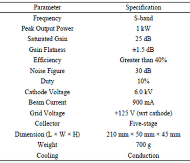
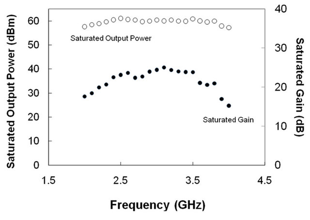
Figure 1. Predicted performance of the compact and lightweight S-band TWT evaluated using large-signal code.

Figure 2. Predicted interaction impedance and normalized phase velocity of the compact and light-weight S-band TWT evaluated using large-signal code.
small in diameter as possible. To achieve maximum gain per length, high perveance beam design is adopted. For high efficiency, the circuit is unloaded over the operating bandwidth. The helix circuit utilizes three circular beryllium oxide (BeO) support rods.
3. Stability
As shown in the Figure 3, an internal helix attenuator (sever loss) is used to suppress internal feedback from the output back to the input, to buffer the input and output RF matches, and to suppress unwanted oscillations. A lossy coating of niobium carbide is applied through a variable density screen to the three BeO rods to create the required internal attenuators for gain and oscillation control. The density of the screen is varied to produce the correct loss profile for internal matching. Niobium carbide has been shown to be resistant to subsequent hydrogen brazes.
4. Circuit
The RF design computations were done in considerable detail in order to determine the optimum choice of operating electrical design parameters. The circuit design starts with setting the desired interaction impedance and phase velocity at the midband of the operating frequency range. The large-signal code was employed to determine the dimensions of helix, support rod, helix tape size, and shell for the required phase velocity and interaction impedance. As shown in Figure 2, at midband, a phase velocity of 0.111 c and an interaction impedance of 67 Ω were obtained. The circuit length and loss pattern are predicted by the large-signal code to obtain the required gain and power. The pitch of the helix along the axial position of the circuit was tapered for efficiency enhancement. Figure 4 shows the optimized pitch profile of the helix circuit obtained from the large-signal code simulations. The helix circuit design parameters are listed
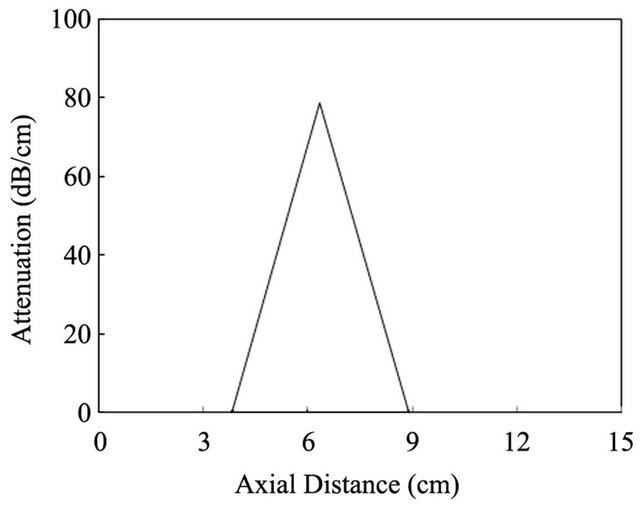
Figure 3. Circuit loss pattern of the compact and lightweight S-band TWT.
in Table 2.
The circuit was assembled using a triangulation assembly technique. The triangulation technique is a method where the tube shell is distorted into a triangular configuration and the helix and rods are slid into place using the extra room inside the shell for ease of assembly. Figure 5 shows the photo of the fabricated S-band helix assembly circuit.
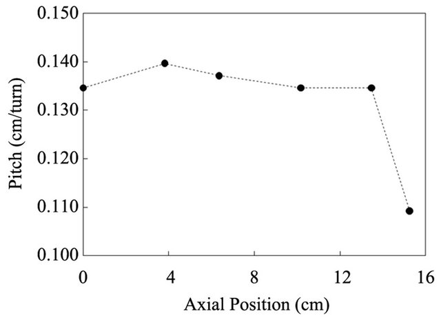
Figure 4. Helix pitch along axial position of the compact and light-weight S-band TWT designed using large-signal code. Helix pitches were tapered for efficiency enhancement.
Table 2. Helix circuit parameters for the compact and lightweight S-band TWT.
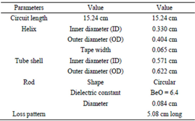
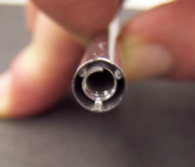
Figure 5. Photo of the assembled helix circuit with three support rods inserted in a stainless steel shell using a triangulation method.
5. Electron Gun
The TWT is driven by a 6.0 kV, 0.9 A electron beam. An electron gun with sufficient current density capable for the 1 kW TWT has been developed. This single-gridded electron gun was designed using EGUN, an electron gun code [8]. The grid transparency, line spacing, line width, and distance from the cathode were carefully chosen to meet beam control requirements.
The electron gun was initially developed using the design synthesis procedure for a Pierce electron gun which was described by Vaughan [9] and then refined using the electron gun code. With the helix set at an inner diameter of 0.330 centimeters, the beam size for a 70% fill factor was 0.231 centimeters. The requirement for a cathode emission density of 1.2 A/cm2 sets the cathode disk diameter at 1.039 centimeters. This yields an area convergence ratio of 20.2:1. Table 3 summarizes the electron gun parameters obtained.
The electrode shapes and the remaining gun dimensions were optimized by numerous computer runs to meet the desired beam parameters at the beam waist with good laminarity. Figure 6 shows the trajectory plot of a computer run for the optimized electron gun design. This gun produces a beam with good laminarity, i.e. the electron trajectories at the beam waist are parallel to each other and evenly spaced.
The mechanical design of the electron gun used the proven stacked ceramic bushing design concept to give a rugged assembly that could be built within the required tolerances. Figure 7 shows a cross sectional view of the electron gun assembly.
Table 3. Gun design parameters for the compact and lightweight S-band TWT.
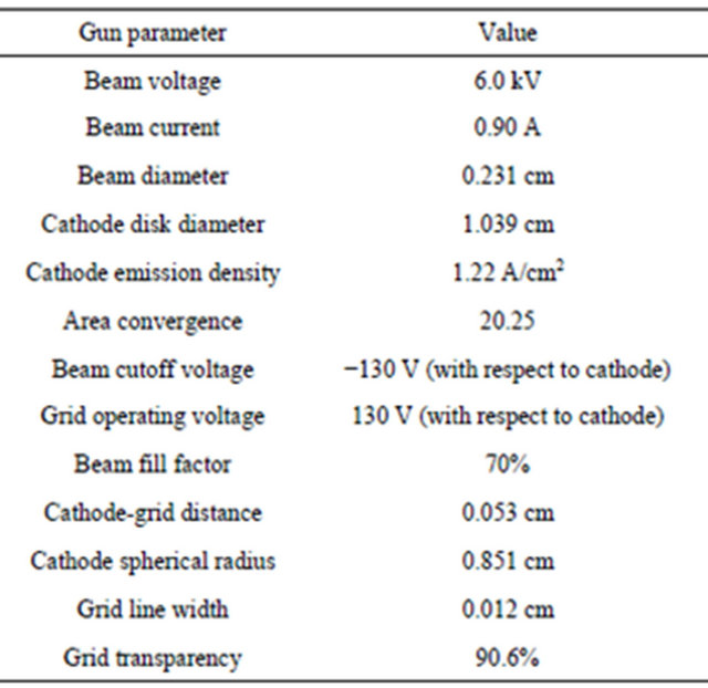
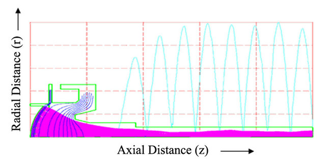
Figure 6. Electron gun trajectory and magnetic field plot evaluated using the EGUN code. Polarity of the magnetic field is not shown.
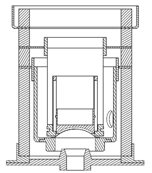
Figure 7. Schematic of a 6.0 kV and 0.9 A electron gun assembly.
6. Periodic Permanent Magnet
The electron beam of the compact and lightweight Sband TWT is focused by a PPM structure. The focusing system was determined using mPPM, a magnetic field stack design code [10] where the design constraints include beam voltage, current, beam diameter, Brillouin field, focusing structure inner diameter, and beam tunnel length. The magnetic field needs to be high enough to contain the electron beam but low enough so that a stable transmission of the electron beam can be provided.
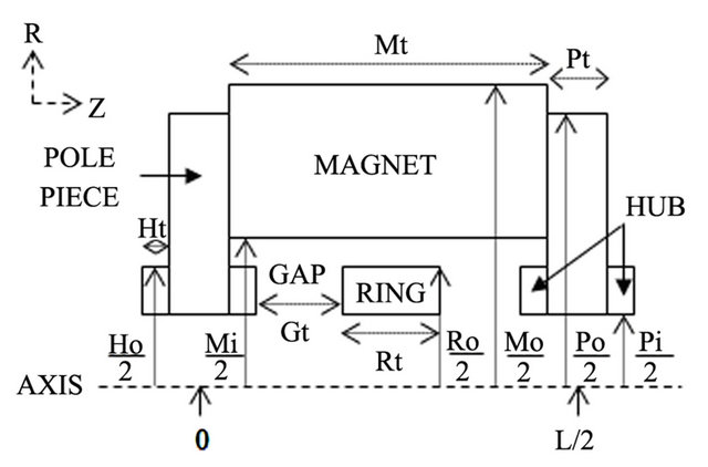
Figure 8(a) shows the cross-sectional drawing of a PPM cell. The dimensions described in the figure determine the magnetic field level in the focusing system. The design parameters are shown in Table 4.
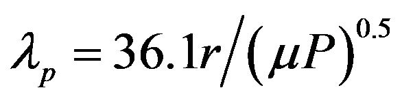
To achieve stiff focusing and to minimize the increase of helix current under drive, it is desirable to set the magnetic period such that the λp/L is greater than 3.0, where λp is the plasma wavelength of the beam and L is the period of the magnet structure. A relation between λp and L can be expressed as
 (1)
(1)
where r is the beam radius and μP is the microperveance. For our design values with a beam radius of 0.117 centimeters and a microperveance of 1.9, the plasma wavelength is 2.954 centimeters. With a magnetic field structure chosen as shown in Table 4, the peak field of 0.153 Tesla was achieved which was required to focus 0.117 centimeters radius beam. The λp/L value which yielded 3.46 promised good focusing with little increase in helix current under drive.
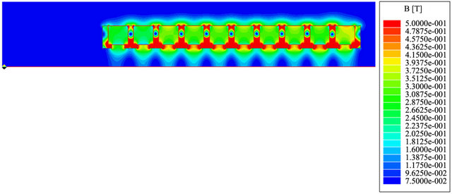
Figure 8(b) shows the cross sectional view of the designed one cell magnet structure with pole pieces and hubs. The magnetic field intensity along the magnet stack was simulated using Maxwell2D, a magnetostatic simulation program [11] and the result is shown in Figure 9(a). Figure 9(b) shows the magnetic field profile along one cell of the magnet stack evaluated.
The focusing magnetic field profile is set up and stacks are temperature stabilized at 300˚C to prevent configuration changes at operating temperatures.
7. Antenna
The impedance matching between the input and output antennas and from the helix to a wave guiding structure through the windows is required. The choices for the wave guiding structure are either a waveguide or a coaxial transmission line, with various configurations for the windows possible, depending on which is chosen. For the compact and lightweight S-band TWT, a coaxial line coupled to the helix with a coaxial ceramic window will be employed since it is sufficient to handle the required power level. A specially designed adapter will be used to convert the RF output to SMA connectors. Figure 10 shows the photo of the antenna assembly.
8. Multi-Stage Depressed Collector (MDC) Using Feedback Current Loops
A five stage depressed collector was designed using 3D PIC code VORPAL [12]. The expected circuit efficiency without the MDC was approximately 19%. By employing a feedback mechanism, an energy recovery efficiency of 70% was achieved. This increased the overall TWT efficiency up to 43.8%. A feedback mechanism provides stable time-dependent voltages to each stages of the depressed collector. Figure 11 shows a schematic of the S-band compact TWT collector assembly. This type of construction provides highly reliable design. The collector has all of the insulating materials that avoids the voltage breakdown but provides the heat flow paths enclosed in a vacuum. Taking into account a possible application requirement, the collector has been realized
Table 4. PPM design parameters for the compact and lightweight S-band TWT.
(a)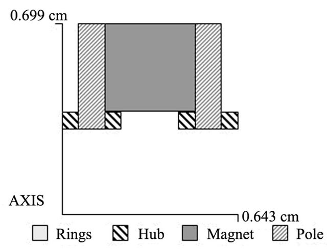 (b)
(b)
Figure 8. (a) Parameters of the one cell periodic permanent magnet and (b) schematic of the periodic permanent magnet for the compact and light-weight S-band TWT designed using mPPM code.
 (a)
(a)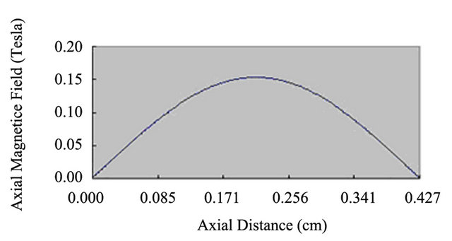 (b)
(b)
Figure 9. (a) Magnetic field distribution along the periodic permanent magnet of the compact and light-weight S-band TWT evaluated using the Maxwell2D code and (b) magnetic field profile along one cell of periodic permanent magnet of the compact S-band TWT.

Figure 10. Photo of the input and output antenna assembly.
with the necessary thermal capacitance to maintain its temperature with cooling that can be accomplished by conduction to a heat sink. Most importantly, the MDC after optimization can fit into the limited space in the compact MPMs.
9. Summary
The integrated design results of a compact and lightweight S-band TWT for a new class of MPMs was de-
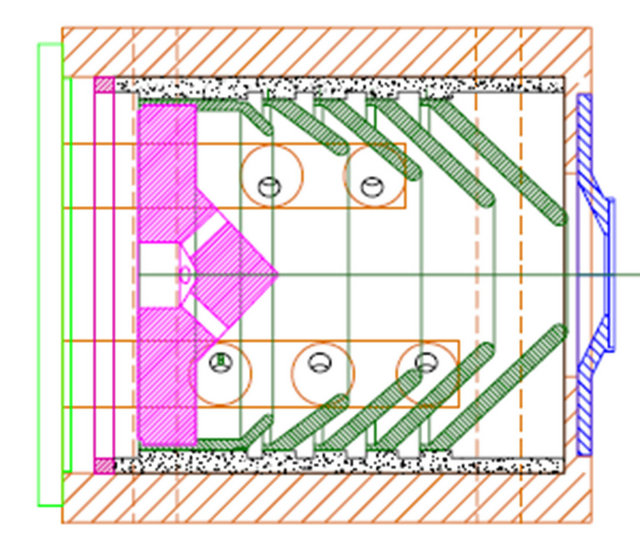
Figure 11. Schematic of the assembly of the five-stage depressed collector for the compact and lightweight S-band TWT.
scribed. The TWT is predicted to generate a saturated output power of greater than 1 kW with a 25 dB saturated gain and over 40% efficiency in S-band. The helix RF circuit assembly consists of a tungsten helix with three circular BeO support rods. The single-gridded electron gun has a convergence ratio of 20.2:1 which will be used to limit the cathode current density. The antennas consist of coax and ceramic window that would directly couple to SMA connector with the use of a specially designed adapter. A five-stage depressed collector has been designed and optimized employing the PIC simulations with a special feedback algorithm. Ceramic insulators and vacuum high voltage feedthroughs will be employed for collector fabrication.
10. Acknowledgements
This work has been supported by the Defense Acquisition Program Administration and Agency for Defense Development.
REFERENCES
- C. R. Smith, C. M. Armstrong and J. Duthie, “The Microwave Power Module: A Versatile RF Building Block for High-Power Transmitters,” Proceedings of the IEEE, Vol. 87, No. 5, 1999, pp. 717-737. doi:10.1109/5.757252
- M. C. Smith, “Comparison of Solid State, MPM, and TWT Based Transmitters for Spaceborne Applications,” Proceedings of the IEEE Southeastcon, Orlando, 24-26 April 1998, pp. 256-259.
- A. Katz, R. Gray and R. Dorval, “Performance of Microwave and Millimeter Wave Power Modules (MPMs) with Linearization,” Proceedings of the IEEE Military Communications Conference, Atlantic City, 17-20 October 2005, pp. 2693-2699. doi:10.1109/MILCOM.2005.1606073
- R. J. Barker, J. H. Booske, N. C. Luhmann Jr. and G. S. Nusinovich, “Modern Microwave and Millimeter-Wave Power Electronics,” IEEE Press, Piscataway, 2005.
- http://www.l-3com.com/
- F. Francisco, “Private Communication,” 2009.
- A. S. Gilmour Jr., “Principles of Traveling Wave Tubes,” Artech House, Norwood, 1994.
- W. B. Herrmannsfeldt, “EGUN: An Electron Optics and Gun Design Program,” SLAC Report SLAC-331, Stanford, 1988.
- J. R. M. Vaughan, “Synthesis of the Pierce Gun,” IEEE Transactions on Electron Devices, Vol. 28, No. 1, 1981, pp. 37-41. doi:10.1109/T-ED.1981.20279
- M. Baird, “mPPM Program Manual User’s Guide,” 2002.
- http://www.ansoft.com/products/em/maxwell/
- C. Nieter and J. R. Cary, “VORPAL: A Versatile Plasma Simulation Code,” Journal of Computational Physics, Vol. 196, No. 2, 2004, pp. 448-473. doi:10.1016/j.jcp.2003.11.004