Journal of Electromagnetic Analysis and Applications
Vol.4 No.4(2012), Article ID:18614,6 pages DOI:10.4236/jemaa.2012.44020
Boundary Induced Inductive Delay in Transmission of Electromagnetic Signals
![]()
1Key Laboratory for the Physics and Chemistry of Nanodevices, Department of Electronics, Peking University, Beijing, China; 2School of Electrical Engineering & Computer Science, Peking University, Beijing, China.
Email: *xusy@pku.edu.cn, *mileslee@pku.edu.cn
Received February 8th, 2012; revised March 7th, 2012; accepted March 15th, 2012
Keywords: Wave Propagation; Computer Modeling and Simulation; Transmission Lines; High-Speed Techniques; Integrated Electronics
ABSTRACT
When an electromagnetic signal transmits through a coaxial cable, it propagates at speed determined by the dielectrics of insulator between the cooper core wire and the metallic shield. However, we demonstrate here that, once the shielding layer of the coaxial cable is cut into two parts leaving a small gap, while the copper core wire is still perfectly connected, a remarkable transmission delay immediately appears in the system. We have revealed by both computational simulation and experiments that, when the gap spacing between two parts of the shielding layer is small, this delay is mostly determined by the overall geometrical parameters of the conductive boundary which connects two parts of the cut shielding layer. A reduced analytic formula for the transmission delay related with geometrical parameters, which is based on an inductive model of the transmission system, matches well with the fitted formula of the simulated delay. This above structure is analog to the situation that an interconnect is between two inter-modules in a circuit. The results suggest that for high speed circuits and systems, parasitic inductance should be taken into full consideration, and compact conductive packaging is favorable for reducing transmission delay of inter-modules, therefore enhancing the performance of the system.
1. Introduction
For modern high-electron-mobility transistors (HEMTs) based on III-V semiconductors e.g. GaAs, GaN, InAs and InSb [1-6], the high-frequency performance is mainly determined by the effective mass of charge carrier and energy gap. However, when these transistors are integrated into circuits or systems, parasitic effects induced by the device structure, interconnects, contacts, and packaging also affect the high-frequency performance of devices [7-11]. Historically, the parasitic impedance of interconnects is neglected and treated as a short. With the scaling down of integrated circuits, the capacitance of interconnects is comparable to the gate capacitance, and the resistance of interconnects increases dramatically, thus RC model for interconnect has been developed [12]. For modern submicron and nanometer electronics, the interconnect inductance also becomes an important factor to be considered. In some cases, current return path and its impact on parasitic inductance etc., are the major factor limiting the performance at high frequency [8,13]. Therefore, neglecting inductance and using an RC model will result in underestimating the propagation delay [14,15].
When high-speed devices, e.g., HEMTs, are operated in the frequency range of 0.5 - 1 THz [1,2,4,16], for instance, its characteristic response time is 1 - 2 picoseconds (ps). In a system consisting of many individual high-speed devices, the characteristic time of the system is then not only determined by individual devices themselves, but also affected by the transmission of electromagnetic (EM) signals between individual devices. The critical length of interconnects is a few tens of microns in 2010 [8], and one may presumably consider that the delay induced by transmission at the speed of light along the interconnects is a few tens of femtoseconds, and therefore is negligible compared with 1 - 2 ps characteristic response time above.
However, we have given a clear picture in this paper that an inductive delay related with boundary conditions will occur and should be taken into account in some situation. To demonstrate this inductive delay, we have constructed a testing system where the shielding layer of a coaxial cable is cut into two parts, leaving a ringshaped small gap, where the copper core wire is still perfectly connected and the two shielding layers are connected and covered by a conductive cylinder. The two parts of the cut coaxial cable represent two individual devices and the copper core wire bridging the gap represents an interconnect. We have revealed by both computational simulation and experiments that, a remarkable delay occurs, and this delay is mostly determined by the overall geometrical parameters of the conductive cylinder when the gap spacing (corresponding to the length of interconnects) is small. Analysis of the results suggests that this delay is inductive.
In this paper of Section 2, we firstly construct a simulated structure of cylinder using high frequency structure simulator (HFSS), and determine the simulated frequency and the criteria of the scattering parameters (S parameters) convergence which are needed for HFSS using finite element method in frequency domain. In Section 3, we scan the structure parameters of the cylinder boundary conditions, and get the delay versus them in Section 3.1, as well as their fitting formula in Section 3.2. Experiments are also done and shown in Section 3.3 to support our simulation. At last we do the experimental analysis by reducing an analytic formula upon the parasitic inductance model in Section 3.4, and it fits well with the fitting formula of the above section, which shows the validity of our model. In Section 4 we conclude our works and show it significance in field of packaging.
2. Methods
2.1. Simulated Structure
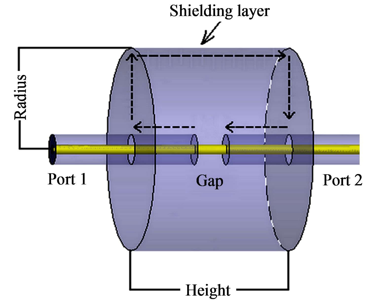
To quantitatively calculate the delay in such a transmission situation, we have simplified the situation by choosing a system with cylindrical symmetry. The simulated system for this work is shown in Figure 1(a), where the shielding layer of a coaxial cable is cut off with a small gap in the middle, and a metallic hollow cylinder is connected to the two parts of the cut coaxial cable, which are located on the axis of the metallic hollow cylinder. So the cylinder shares the same ground with the two parts of the cable. The gap spacing is d, and the height and radius of the cylinder are H and R, respectively. In our simulation, the two cables are treated as individual devices, and the wire bridging the gap is treated as an interconnect. Figure 1(b) is a simplified equivalent circuit of such a structure.
2.2. Simulated Frequency
To precisely measure the delay for EM signals propagate ing from Port 1 to Port 2 as shown in Figure 1(a), one can use a pulsed signal, and compare the difference of transmission time with a reference coaxial cable of the same length, as reported in previous experiments [17]. In
 (a)
(a)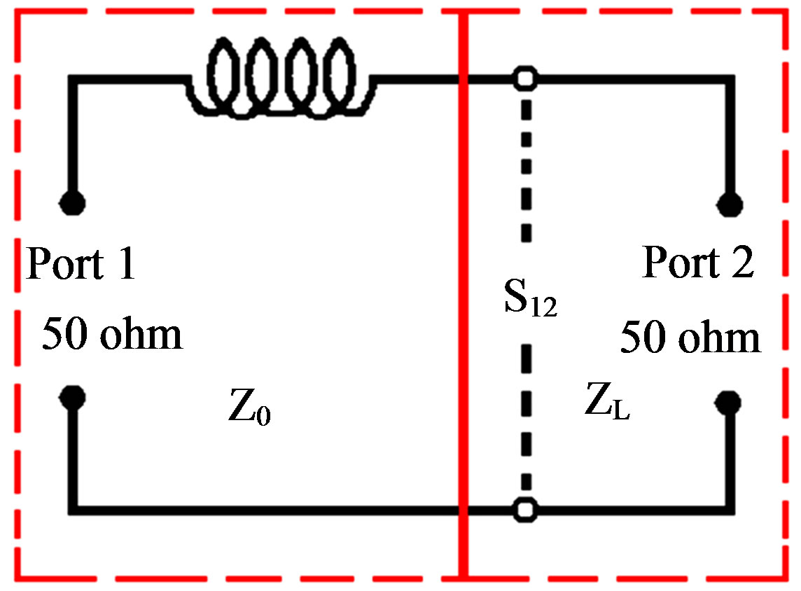 (b)
(b)
Figure 1. (a) Schematic of the system for simulation. A gap is set between two coaxial cables. The two cables are just connected with a core wire. An outer cylindrical metallic box surrounds the gaped region, and is grounded to shielding layers of both cables; (b) The equivalent circuit of the system in (a). The effect of outer cylindrical box on the core wire bridging the gap is counted as inductance. The impedance values of Port 1 and Port 2 are both set at 50 ohm.
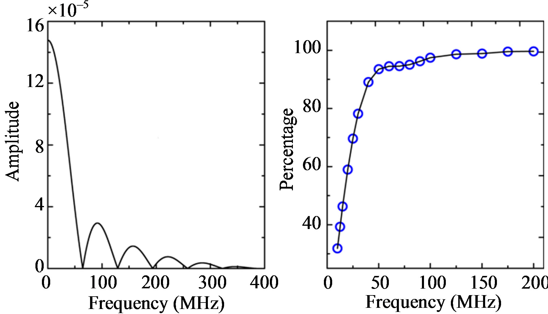
these experiments, the pulses have typical rise time and fall time around 2.5 ns, and a duration time around 13 ns. The frequency spectrum of such a pulse up to 400 MHz is shown in Figure 2(a) obtained by fast Fourier transformation (FFT) in Matlab codes. In the frequency spectrum, we have calculated the ratio of energy below specific frequencies to the whole energy, shown in Figure 2(b). And we set 100 MHz whose ratio is 97.43% as the highest frequency limit for calculating the transmission behavior of the pulse, assuming that our simulation with this cutoff of the spectrum will give results precise enough to approximate the real situation [9].
2.3. Criteria of S Parameters for Matrix Convergence
We have applied the HFSS to perform the situation. The HFSS uses the finite element method to mesh the simulated structure and a criterion is needed to decide the convergence. We use both maximum deltas of the magnitude of S parameters (Mag S) and the phase of S parameters (Phase S) as the criteria for the matrix convergence because calculating of group delay is acquired.
A proper criterion of Mag S should be small enough so as to obtain sufficient accuracy, but not too small to avoid unnecessary long computational time. We set the criteria as 1 × 10⁻³ and 5 × 10⁻³, respectively. Figure 3 plots the relative deviations of the corresponding Mag S to that for a criterion of 1 × 10⁻⁴. The relative deviations are all less than 0.016% below 100 MHz showing a good convergence. Therefore we set the final criterion as 1 × 10⁻³, which is proven to be small enough for a desired accuracy of the simulations.
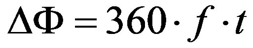
The criterion of Phase S is more closely related to calculation of the group delay. At a specific frequency f, shift of phase ΔΦ, is given as:
 (1)
(1)
where Δt is defined as the group delay. In our previous experimental setup for measuring the delay in transmission of pulsed signals, the time resolution of the measurement system is about 10 ps [17]. If Δt is set as 10 ps, its corresponding phase shift is 3.6 × 10⁻⁹ f. For simplicity and higher accuracy, we set the criterion of Phase S as 1 × 10⁻⁹ f, which corresponds to a time resolution about 3 ps.
 (a) (b)
Figure 2. (a) The frequency spectrum of the periodic pulse up to 400 MHz; (b) The percentage of energy over the whole energy below series of frequencies.
 (a) (b)
Figure 3. The relative deviation of magnitude of S parameters when the delta of Mag S set as 1 × 10⁻³ and 5 × 10⁻³ compared with 1 × 10⁻⁴.
3. Results and Discussion
3.1. Relationship of Delay versus Frequency and Gap
By using the set criteria, we have systematically simulated the group delay of sine waves of varied parameters of frequency f, gap spacing d, height H and radius R of the cylinder.
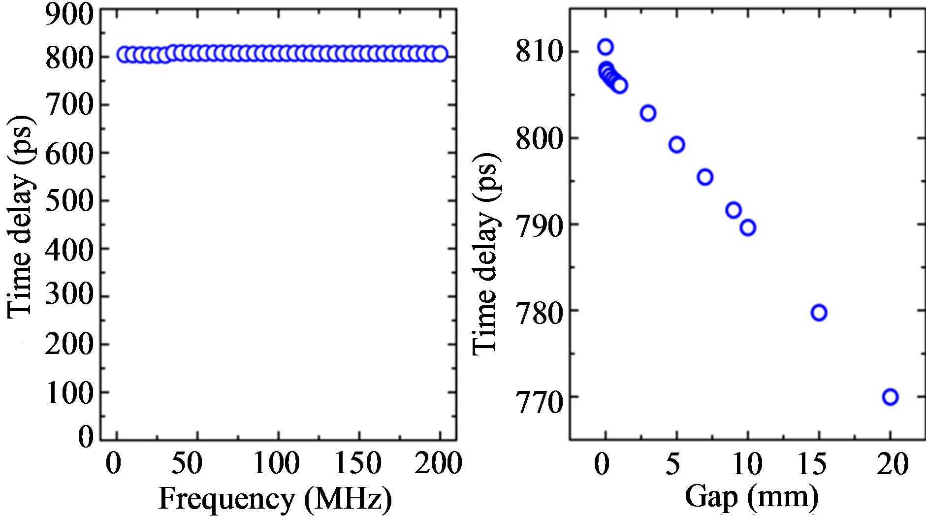
The group delay of sine waves of varied f with fixed d, H and R have been simulated. Figure 4(a) plots typical results, where H = 20 mm, R = 15 mm, and d = 0.1 mm. In these conditions, we find that the group delay is almost independent of frequency up to 200 MHz. Therefore, we set the frequency at 100 MHz for simulations hereafter, and the group delay calculated at this frequency can represent well for the delay of a nano-second EM pulse.
Although we have used pulsed signals instead of high frequency excitations in the simulation, and after Fourier transformation of the pulses the cut-off frequency of the spectra is set at only 100 MHz (see Figure 2), the results of this work should be still valid for modern high speed electronic systems working at 100 - 1000 GHz. This is because, what we have calculated is the absolute transmission delay independent of frequencies, assuming that in vacuum all electromagnetic waves with varied frequencies travel at the same speed, causing the same delay for same distance.
The calculated delay is found dependent on the gap spacing d. Figure 4(b) plots typical results of the group delay of sine waves of varied d, where f = 100 MHz, H = 20 mm and R = 15 mm. When d is smaller than 1.0 mm, the simulated delay time is almost a constant.
3.2. Relationship of Delay versus Height and Radius of the Cylinder
Finally, we set d = 0.1 mm so that we can ignore the in-
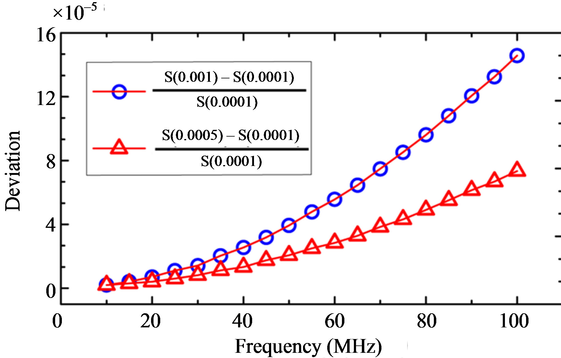
Figure 4. (a) The simulated data of delay versus frequency f with fixed H = 20 mm, R = 15 mm, and d = 0.1 mm; (b) The simulated data of delay versus gap spacing d, with fixed f = 100 MHz, H = 20 mm and R = 15 mm.
fluence of gap spacing for more quantitative simulations on varied H and R. The height H is assigned to vary from 2 mm to 60 mm with step of 2 mm. The radius R is assigned to vary from 2 mm to 30 mm with step of 1 mm.
The results are plotted in Figure 5 in a 3-dimensional (3D) frame. The results show a good linear correlation between the delay τ0 and height H at fixed R, but the correlation between the delay τ0 and radius R at fixed H is nonlinear.
The slope of τ0 versus H is related with R. So the fitting formula should have the form,
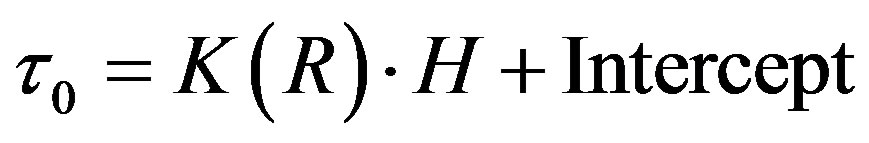 (2)
(2)
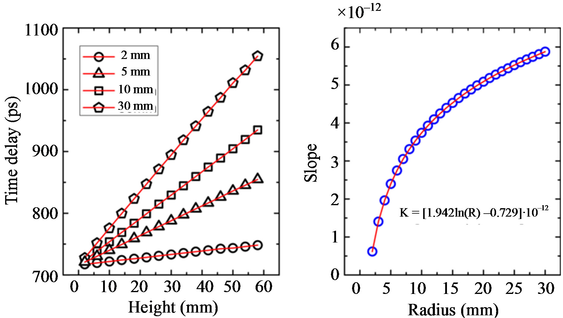
where K(R) is the slope at specific R, and Intercept is the interception. Figure 6(a) plots simulated data of τ0 versus H at some fixed values of R at 2.0, 5.0, 10.0 and 30.0 mm, respectively. The four straight lines can fit well with these data separately in the figure. Figure 6(b) plots the data of K(R) versus R, as derived from the data shown in Figure 5. In this figure, a solid curve fits well to the data, following the formula:
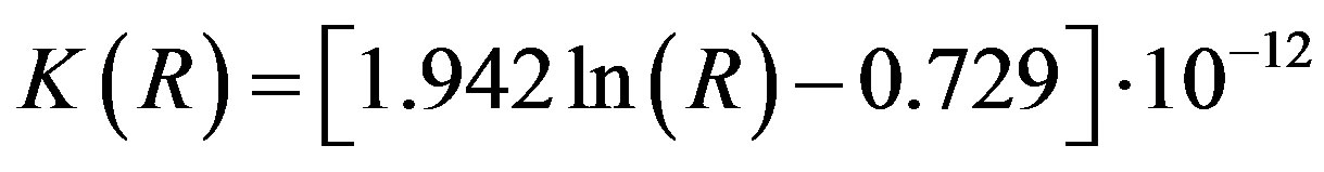 (3)
(3)
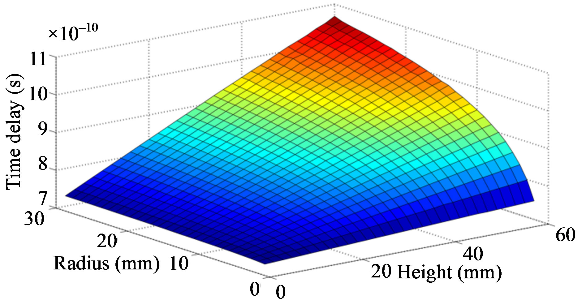
Figure 5. The simulated data of delay versus cylinder height H and radius R, at fixed frequency f = 100 MHz and gap spacing d = 0.1 mm.
 (a) (b)
Figure 6. (a) Open markers are the simulated delay versus height at fixed R of 2.0, 5.0, 10.0 and 30.0 mm, respectively. The fittings are plotted with red lines; (b) Blue open circles are simulated slopes at varied radius. The fitting red line is following the formula given in the figure.
Next, by using similar formula, we try to fit all the simulated data shown in Figure 5. A modified general formula is therefore derived as:
 (4)
(4)
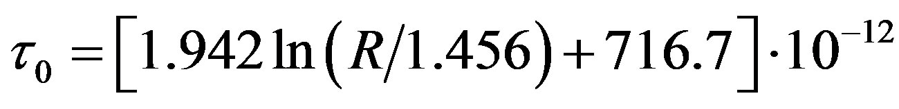
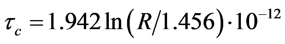
This fitting matches the simulated data perfectly, where the maximum absolute deviation in τ0 is only ±5 ps. Here we find the interception of 716.7 ps is very close to the transmission time of 716.1 ps along a perfect coaxial cable of 150 mm, which is equal to the total length of the two cables shown in Figure 1(a). To confirm this, we have changed the cable length between Port 1 and Port 2 to 60 mm, 100 mm and 120 mm, and the interceptions of the fitting results are all very close to the corresponding transmission time. So we conclude that this interception is arisen from the transmission time through the two coaxial cables. Further, the first part of Equation (2) should be the delay caused by EM signals transmitting through the metallic cylinder seen from the two sides of the gap. We define it as τc, which gives
 (5)
(5)
For modern high speed electronic systems working at 100 - 1000 GHz, their characteristic time scale is at 1 - 10 ps. The simulated transmission delay is in order of 10 ps for boundary dimension of 10 mm, as shown in Figure 6, therefore is large enough to be taken into consideration.
3.3. Comparison between the Experimental and Simulated Data
We also have done experiments to measure the time delay using this structure in our previous work [17], and compared the experimental and simulated data, shown in Figure 7. The simulated delay is higher than the experimental data mostly. It may be resulted from our subjective definition of the pulse delay, where we used the 10% rising time of pulse as reference point. However, one can see that the linear relationship between the delay and height is in agreement in both the experimental and simulated data.
3.4. Experimental Result Analysis
Now we try to give a phenomenological explanation of the results. We assume the boundary condition around the gap has induced an additional inductance. Because the interception equals to the transmission time of the cable, the electromagnetic wave should transmit to one end of the gap, and then transmit through the cylinder, and finally pass through the other end of the gap. From the perspective of current, the current path is schematically highlighted with arrowed dotted lines shown Figure 1(a), similar to that of a coaxial cable. By using the
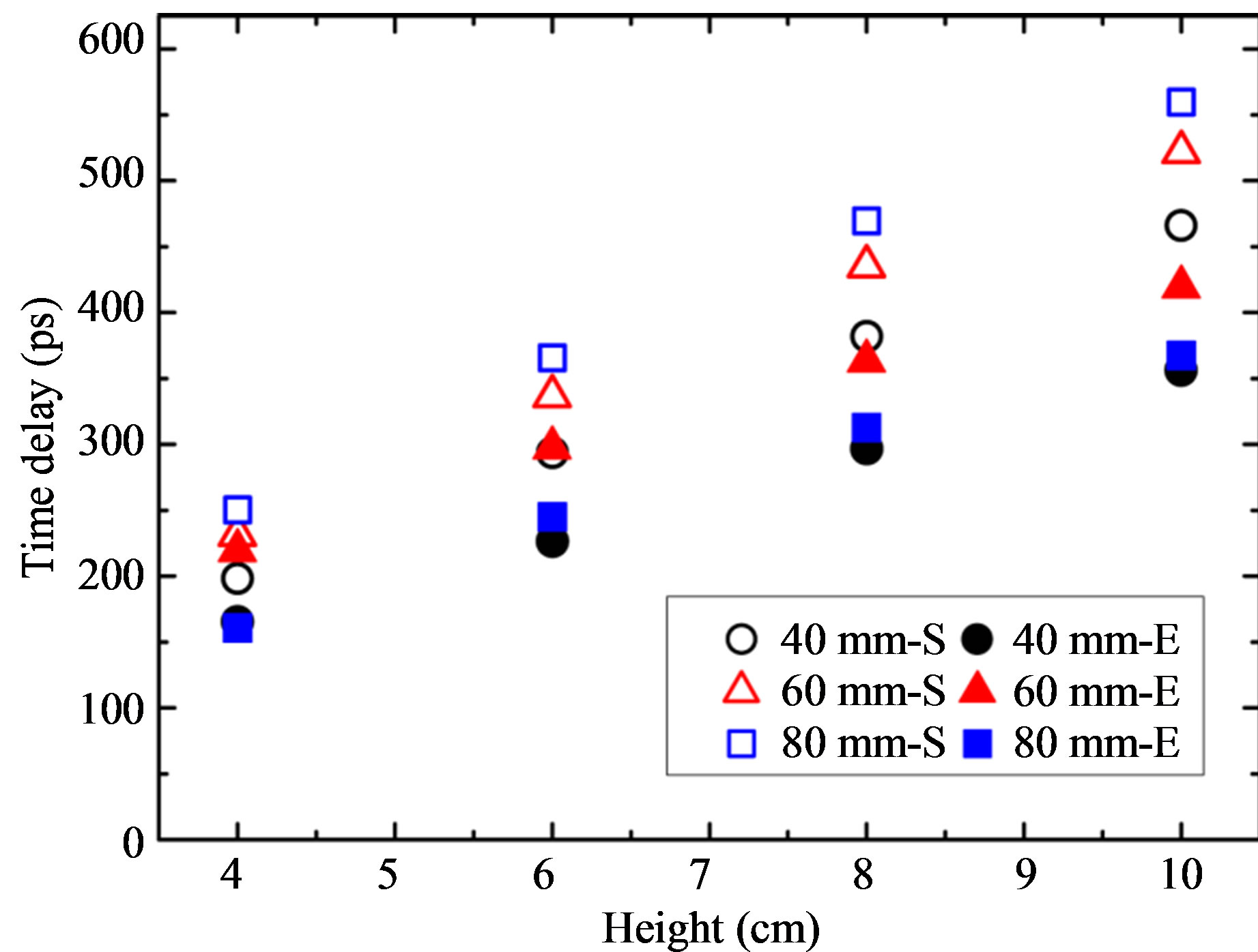
Figure 7. The comparison data between the simulated and experimental data. 40 mm, 60 mm and 80 mm are the diameters of the cylinder respectively. S represents simulation, and E represents experiment. The gap is 0.1 mm both in the experiment and simulation.
inductance formula for a coaxial cable, we calculate the inductance in our simulated structure as:
 (6)
(6)
where R is the radius of the cylinder, and R0 is the outer radius of the coaxial cable, and μ is the space permeability with value of 4 × 10⁷ H/m. The equivalent circuit of the fixture is shown in Figure 1(b). We use the formula of transmission coefficient of electromagnetic wave theory [18]. It gives:
 (7)
(7)
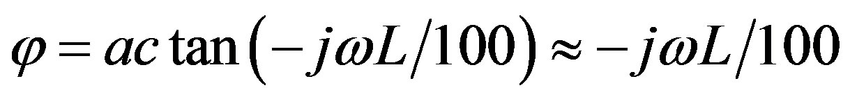
where T is the transmission coefficient, Z0 = (50 + jωL)Ω is the impedance seen from port 2, and ZL = 50 Ω is the impedance seen from port 1. Assume ωL  100, then
 (8)
(8)
and
 (9)
(9)
For ωL  100, (ωL/100) is very small. Equation (9) can be approximated,
 (10)
(10)
The group delay can be obtained from the formula,
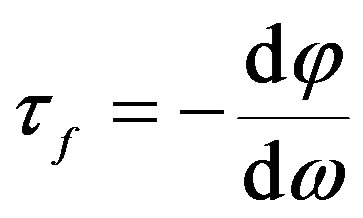 (11)
(11)
Taking (10) and (6) into (11), it gets
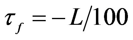 (12)
(12)
Taking μ = 4 × 10⁷ H/m and R0 = 1.5 mm, it can be deduced
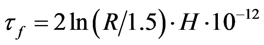 (13)
(13)
We can see the deduced Equation (13) and the fitted Equation (5) are very similar to each other. This confirms that the delay time is resulted from the parasitic inductance of the additional cylinder shielding around the gap. The parasitic inductance can be calculated using the inductance formula of a coaxial cable.
4. Conclusion
By using HFSS simulation, this work clearly reveals the origin of a boundary dependent delay in transmission of an electromagnetic signal between two coaxial cables with a small open gap in their shielding layers. For a metallic boundary with cylindrical symmetry, we have obtained an analytical formula for this delay, which matches well with the simulation results, showing that this delay has an inductive nature, although for the first glance one may assume this delay is introduced by parasitic capacitance of the system. As the performance of high-speed electronic systems relies on both the processing speed of individual devices and the transmission delay time between inter-modules, it resembles the cask effect that large transmission delay between inter-modules can limit the system performance dramatically. On the one hand, reducing the dimension size of the boundary along the transmission axis can reduce the delay effectively. On the other hand, reducing the dimension size of the boundary conditions can increase the parasitic capacitance of the system which can also limit the system performance. This can be helpful in the comprehensive consideration of parasitic inductance and parasitic capacitance [13]. Our results imply that reducing the dimension size of the boundary along the transmission axis can reduce the delay effectively and a induced formula can give some guidance for the design of the boundary conditions; therefore compact metallic packaging may help in cutting the transmission delay between intermodules to some extent.
5. Acknowledgements
We thank W. Q. Sun in Peking University for valuable discussions. This work was supported by MOST of China (Grant No 2011DFA51450 and 2011CB933002), and NSF of China (Grants 11074010).
REFERENCES
- S.-J. Yeon, M. Park, J. Choi and K. Seo, “610 GHz InAlAs/In0.75GaAs Metamorphic HEMTs with an UltraShort 15-nm-Gate,” IEEE International Electron Devices Meeting, 2007, pp. 613-616.
- W. Snodgrass, W. Hafez, N. Harff and M. Feng, “Graded Base Type-II InP/GaAsSb DHBT With fT = 475 GHz,” IEEE Electron Device Letters, Vol. 27, 2006, pp. 84-86.
- Y. F. Zhang and J. Singh, “Charge Control and Mobility Studies for an AlGaN/GaN High Electron Mobility Transistor,” Journal of Applied Physics, Vol. 85, No. 587, 1999, pp. 587-594. doi:10.1063/1.369493
- Y. Yamashita, A. Endoh, K. Shinohara, K. Hikosaka, T. Matsui and S. Hiyamizu, “Pseudomorphic In0:52Al0:48As/ In0:7Ga0:3As HEMTs with an Ultrahigh fT of 562 GHz,” IEEE Electron Device Letters, Vol. 23, No. 10, 2002, pp. 573-575. doi:10.1109/LED.2002.802667
- R. J. Trew, “High-Frequency Solid-State Electronic Devices,” IEEE Transactions on Electron Devices, Vol. 52, No. 5, 2005, pp. 638-649. doi:10.1109/TED.2005.845862
- L. D. Nguyen, P. J. Tasker, D. C. Radulescu and L. F. Eastman, “Characterization of Ultra-High-Speed Pseudomorphic AlGaAs/InGaAs (on GaAs) MODFET’s,” IEEE Transactions on Electron Devices, Vol. 36, No. 10, 1989, pp. 2243-2248. doi:10.1109/16.40906
- International Technology Roadmap for Semiconductors, Assembly and Packaging, 2009.
- International Technology Roadmap for Semiconductors, Interconnect, 2009.
- R. Achar and M. S. Nakhla, “Simulation of High-Speed Interconnects,” Proceedings of the IEEE, Vol. 89, No. 5, 2001, pp. 693-728. doi:10.1109/5.929650
- T. Liang, J. A. Plá, P. H. Aaen and M. Mahalingam, “Equivalent-Circuit Modeling and Verification of Metal-Ceramic Packages for RF and Microwave Power Transistors,” IEEE Transactions on Microwave Theory and Techniques, Vol. 47, No. 6, 1999, pp. 709-714. doi:10.1109/22.769340
- F. Schwierz, “Graphene Transistors,” Nature Nanotechnology, Vol. 5, No. 7, 2010, pp. 487-496.
- A. Brambilla, P. Maffezzoni, L. Bortesi and L. Vendrame, “Measurements and Extractions of Parasitic Capacitances in ULSI Layouts,” IEEE Transactions on Electron Devices, Vol. 50, No. 11, 2003, pp. 2236-2247. doi:10.1109/TED.2003.818150
- L. David, C. Crégut, F. Huret, Y. Quéré and F. Nyer, “Return Path Assumption Validation for Inductance Modeling in Digital Design,” IEEE Transactions on Advanced Packaging, Vol. 30, No. 2, 2007, pp. 295-300. doi:10.1109/TADVP.2007.896002
- Y. I. Ismail, “On-Chip Inductance Cons and Pros,” IEEE Transactions on Very Large Scale Integration (VLSI) Systems, Vol. 10, No. 6, 2002, pp. 685-694.
- A. Brambilla and P. Maffezzoni, “Statistical Method for the Analysis of Interconnects Delay in Submicrometer Layouts,” IEEE Transactions on Computer-Aided Design of Integrated Circuits and Systems, Vol. 20, No. 8, 2001, pp. 957-966.
- F. Schwierz and J. J. Liou, “RF Transistors: Recent Developments and Roadmap toward Terahertz Applications,” Solid-State Electronics, Vol. 51, No. 8, 2007, pp. 1079-1091. doi:10.1016/j.sse.2007.05.020
- S. Y. Xu, Y. Yang, D. F. Pei, X. Zhao, Y. X. Wang, W. Q. Sun, B. Ma, Y. Li, S. S. Xie and L.-M. Peng, “A WaveGuide-Like Effect Observed in Multiwalled Carbon Nanotube Bundles,” Advanced Functional Materials, Vol. 20, No. 14, 2010, pp. 2263-2268. doi:10.1002/adfm.201000263
- D. M. Pozar, “Microwave Engineering,” 3rd Edition, John Wiley & Sons Inc., New York, 2005.
NOTES
*Corresponding authors.