Engineering
Vol.4 No.12A(2012), Article ID:26067,16 pages DOI:10.4236/eng.2012.412A118
Mitigation of Human Exposure to Electromagnetic Fields Using Carbon Foam and Carbon Nanotubes
Department of Astronautic, Electric and Energy Engineering, Sapienza University of Rome, Rome, Italy
Email: davide.micheli@uniroma1.it
Received August 17, 2012; revised September 20, 2012; accepted October 2, 2012
Keywords: Carbon Nanotube; Carbon Foam; Layered Materials; Radar Absorbing Material; Winning Particle Optimization; Human Exposure Mitigation
ABSTRACT
In recent years there has been increasing concern about the possible consequences on human health from exposure to RF fields produced by wireless telecommunication technologies. In this work the coupling between carbon foam and composite materials made of carbon nanotubes and epoxy-resin allows to build a material able to absorb the electromagnetic field thus reducing its intensity in the environment where the mitigation of electromagnetic field is required. The Frequency range considered is 2 GHz - 3 GHz which is the most common frequency band used in wireless network and microwave oven too. Two different kind of heterogeneous materials are designed, one is a layered radar absorbing material made exclusively of epoxy resin and carbon nanotube in different weight percentage, the others are porous carbon foam where the pores are supposed be filled with carbon nanotubes and epoxy-resin. Both type of materials show interesting absorption properties reaching peak of reflection coefficient between –15 dB and –45 dB for a normally incident plane wave.
1. Introduction
International exposure guidelines have been developed to provide protection against established effects from RF fields by the International Commission on Non-Ionizing Radiation Protection (ICNIRP) [1] and the Institute of Electrical and Electronic Engineers (IEEE, 2005) [2].
Some people perceive risks from RF exposure as likely and even possibly severe. Several reasons for public fear include media announcements of new and unconfirmed scientific studies, leading to a feeling of uncertainty and a perception that there may be unknown or undiscovered hazards [3].
The World Health Organization (WHO) established the International EMF Project in 1996 to assess the scientific evidence of possible health effects of electromagnetic field (EMF) in the frequency range from 0 to 300 GHz. EMF Project, has established a programme to monitor the EMF scientific literature, to evaluate the health effects from exposure to EMF, to provide advice about possible EMF hazards and to identify suitable mitigation measures. While no health effects are expected from exposure to RF fields from base stations and wireless networks, research is still being promoted by WHO to determine whether there are any health consequences from the higher RF exposures from mobile phones [4].
In this paper the mitigation of electromagnetic field intensity in the frequency range 2 GHz - 3 GHz is approached applying the absorption of the electromagnetic fields. Absorption of electromagnetic fields is commonly exploited in radar absorbing materials (RAM) [5], and in this context the RAM could be applied on the wall of the environment in which the mitigation of electromagnetic field is required. The simulation of the absorption mechanism was obtained through different materials, one is a layered nanostructured composite materials, the others are carbon foam in which the pores are supposed be filled with multiwalled carbon nanotubes (MWCNT), homogeneously dispersed in the epoxy-resin with a filler concentration of 1 wt%. The nanostructured layered composite material is made of epoxy-resin filled with different weight percentage of MWCNT. Here the thickness and filler concentration of each layer has been optimized using the recent introduced winning particle optimization (WPO) [6,7] algorithm. In particular, WPO was applied to six different materials made of epoxy-resin with a filler weight concentration of 0, 0.5, 1, 1.5, 2.5 wt% of MWCNT. Measurements of electrical permitivity of the six materials as a function of frequency were stored in a database in order to supply data to the WPO algorithm. WPO in turn is deputed to design and optimize the layered composite material by minimizing an objective function in which the reflection coefficient, and the thickness of RAM are the main factors taken into account [7].
The other RAM were simulated by the numerical modeling of two different type of carbon foam morphology. Due to its porosity carbon foam is able to gradually absorb the electromagnetic wave [8,9], and an enhancement of such effect was here analyzed by simulating the pores of the foam as filled with carbon nanotubes dispersed in the epoxy-resin with a filler concentration of 1 wt%. In particular this last effect was studied by finite element method (FEM) using the COMSOL Multiphysics commercial code [10] where the dielectric properties of filler have been previously measured for the six different nanostructured composite materials. The paper is organized in the following way: Section 2 reports the description of manufacturing of nanostructured composite materials, the Section 3 reports the dielectric measurements of nanostructured composite materials, the Section 4 describes the simulation of the nanostructured layered material and of the related electromagnetic absorbing, the Section 5 reports the FEM analysis of the RAM made of carbon foam and MWCNT.
2. Manufacturing of Nanostructured Composite Materials
Industrial grade MWCNTs with commercial name of NANOCYLTM NC7000 (diameter around 9.5 nm, length 1.5 µm, purity 90%) were bought at NANOCYL. Bi-component Epoxy-resin PrimeTM 20 LV (density 1.123 g/cm3) with Hardner (density 0.936 g/cm3) was used as matrix. RAM is based on layered materials where each layer is made of carbon nanostructured composites materials in different weight percentages. The first step was to build little samples of composite material in order to compute the relative permittivity as a function of frequency of applied electromagnetic field. Retrieval of the dielectric parameters was obtained measuring microwave scattering parameters S11, S21, S12, S22, by means of vector network analyzer and a coaxial transmission line method. The shape and the dimensions of coaxial probe determined those of composite materials samples. Agilent 7 mm, 50 OHM AIRLINE type 85051 is the probe. In order to prepare the cylindrical samples a perforated plate of aluminum was used for casting the composite materials in the fluid state. Each hole of the plate can accommodate a sample. In Figure 1 schematics of the perforated plate, a picture of the coaxial airline and the connection of vector network analyzer to the coaxial airline are shown. Basically carbon nano-filler was uniformly dispersed in the resin at different weight percentages (0, 0.5, 1, 1.5, 2, 2.5 wt%).
A critical point is achieving nanoparticles dispersion in
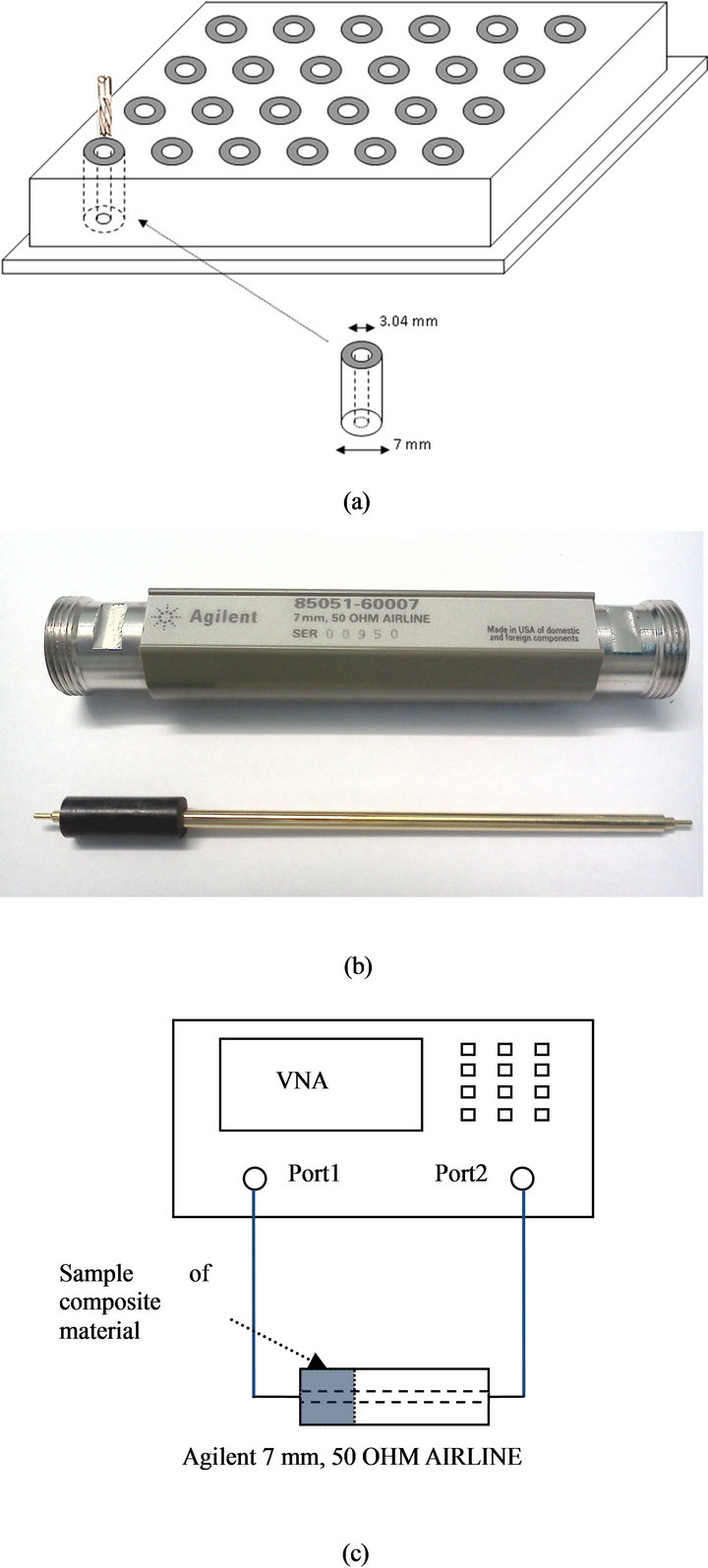
Figure 1. (a) Schematics of the perforated plate; (b) Picture of the Agilent 7 mm, 50 OHM AIRLINE type 85051; (c) Agilent PNA connected to Agilent 7 mm, 50 OHM AIRLINE.
the resin with a homogeneous and isotropic distribution. This is due to the Van Der Walls [11] forces that tend to aggregate the nanoparticles to each other. In materials preparation, the dispersion of the carbon nanomaterials within the polymer matrix was achieved by sonication at room temperature. The sonication was carried out at 20 kHz for about 15 min by means of Sonics Ultransonicator (VCX750 model), setting 20% amplitude with respect to the full-scale oscillation magnitude of ultrasonic processor. The polymerization takes about 16 hours at 50˚C temperature. The resulting composites samples have been dielectrically characterized to recover the dielectric properties of the composite materials in the data base (DB).
3. Dielectric Characterization of Nanostructured Composite Materials
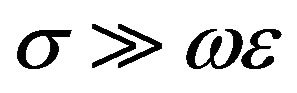
Measurement setup consists of a vector network analyzer (VNA) Agilent PNA-L N5230C working up to 20 GHz, Agilent airline and related calibration kit in the band (2 - 18 GHz), the above mentioned sample holder hosting the materials under test (MUTs); the length of sample holder is 20 mm. Two-port measurements are applied. We retrieved the electrical permittivity of samples by processing the VNA scattering parameters Sij raw data with different numerical algorithms. The adopted algorithms are Nicholson-Ross [12], National Institute of Standards and Technology (NIST) iterative [13], and non-iterative [14]. All these algorithms are available in the software package of Agilent measurement software (Agilent software 8571E material measurement). Declared accuracy is 2%. The three methods were applied on four samples of each kind of materials and they give almost identical results, thus confirming both: estimation and measuring setup goodness. Materials react to applied electromagnetic field in a variety of ways includeing displacements of both free and bound electrons by electric fields and the orientation of atomic moments by magnetic fields. Often the responses are independent from the direction of the applied field and the material is called isotropic [15]. The responses of these linear, isotropic materials to time-varying fields may depends to a significant extent on the frequency of the fields. The terminology is also important with time-varying fields, we use the terms dielectrics, conductor, to indicate the character of the dominant response since in absolute terms does not exist a perfect conductor or a perfect dielectric but only lossy dielectrics. The character is strongly related to the frequency of the electromagnetic field we are considering. Observing the Maxwell equation of the magnetic field H, it can be assumed a simple meaning of the dominant response of a certain materials. In the Equation (1), H is the magnetic field, E is the electric field, w is the angular frequency, s is the electrical conductivity, e0 is the permittivity of vacuum and er is real part of the relative electric permittivity, the ratio s/jwe0 represent the imaginary part of the electrical permittivity. The terms J represent the conduction current whereas the term jweE represent the displacement current.
 (1)
(1)
 .
.
The dominant character of a materials is like that of a conductor if the conduction current is greater than the displacement current
 (2)
(2)
As known the electrical permittivity of a materials is a complex number [16-18], describing the interaction of a material with an electric field. The real part of permittivity is a measure of how much energy from an external electric field is stored in a material. The imaginary part of permittivity is called the loss factor and is a measure of how dissipative or lossy a material is to an external time-varying electric field. The imaginary part of permittivity is always greater than zero and is usually much smaller than real part. The loss factor includes the effects of both dielectric loss and conductivity that contribute to its overall permittivity. Both permittivity and permeability are complex but not constant (a reason why the term dielectric constant is ambiguous). Many materials exhibit considerable change over frequency and temperature.
Some materials such as iron (ferrites), cobalt, nickel and their alloys have appreciable magnetic properties for which it is valuable to measure permeability; however, many materials are non-magnetic. A dielectric material has an arrangement of electric charge carriers that can be displaced by an electric field. The charges become polarized to compensate for the electric field such that the positive and negative charges move in opposite directions.
At the microscopic level, several dielectric mechanisms can contribute to dielectric behavior [19]. Dipole orientation and ionic conduction interact strongly at microwave frequencies. Water molecules, for example, are permanent dipoles, which rotate to follow an alternating electric field. These mechanisms are quite lossy—which explains why food heats in a microwave oven. Atomic and electronic mechanisms are relatively weak, and usually constant over the microwave region [20,21].
In Figure 2, the real and the imaginary part of relative permittivity are plot for all the composite materials. As far as nanomaterials are concerned it can be highlighted how an increase in the filler weight percentage determine the growth of the value of real and imaginary part of electrical permittivity. In particular the losses in the nanostructured composite materials can be also related with the electrical conductivity at microwave frequencies, the higher the concentration of filler, the greater the
 (a)
(a) (b)
(b)
Figure 2. (a) Real part of relative electrical permittivity of nanostructured composite materials; (b) Imaginary part of relative electrical permittivity of nanostructured composite materials.
amount of conductive paths made by MWCNT. This in turns increases the localization and the dissipation phenomena giving rise to the absorption of microwave.
4. Simulation of the First Type of RAM Made of Layered Nanostructured Composite Materials
This section stars with the electromagnetic definition of intrinsic wave impedance of multilayer plane.
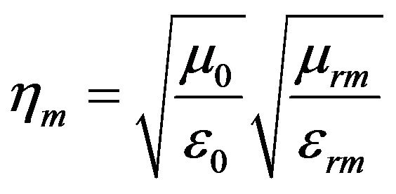
The wave number of generic mth-dielectric-layer  depends on dielectric characteristics of materials and the angular frequency. For the generic mth-layer and the wave the characteristic wave impedance [22] is defined as
 (2)
(2)
where µ0 is permeability of vacuum, µrm is the relative permeability of mth-material. Starting from this definition the theory of multilayer plane has been developed and the WPO algorithm applied. The complete formulation of the mathematical model of multilayer plane and the application of WPO algorithm to the RAM design and optimization can be found in [7-22]. In particular, given a certain database of composite materials and a certain frequency band, the main problem we want to solve is to find the best multilayer material architecture able to minimize the electromagnetic reflection coefficient for all the frequencies in the band and possibly for all the incidence angles and contemporarily try to reduce as much as possible the overall thickness of multilayer materials. As a consequence design a layered material means to find the best answer to the following questions:
• How many layers are needed?
• Which is the best composite material for each layer?
• Which is the optimal thickness of each layer?
Probably there are different combinations able to determine a satisfactory solution. This task is not easy to be solved manually by trial and errors since there are infinite combinations to be tested. One scientifically valid approach is to use evolutionary computation and/or swarm intelligence to find the optimal solution. In this work the WPO algorithm was applied.
The optimized RAM is made of two layers one of MWCNT-2.5 wt% and another of epoxy-resin. Figure 3 shows the schematic of RAM and Figure 4 shows the reflection coefficient. It can be noticed that the optimized RAM shows the highest absorption capability around the center of frequency band where the reflection coefficient is around –45 dB. The two main absorption mechanisms are due to the lowering of the impedance mismatch between free space and RAM and to the maximization of losses inside the RAM. The first one can be optimized by choosing an adequate thickness of each layer and the second one by choosing materials with higher dielectric losses. Unfortunately both mechanisms are simultaneously present and it is not possible to work on the first one of them without affecting the other one. This is why an optimization technique which is able to take into account for both mechanisms is needed to obtain the best performance.
5. Simulation of the Second Type of RAM Made of Carbon Foam Filled with Carbon Nanotubes and Epoxy-Resin
Carbon foams are cellular structures with low mass density [23]. Their mechanical, thermal and electrical properties are strictly dependent on cell size, shape and 3-D arrangement [24]. These cell parameters determine the specific bulk material properties, the relative density and porosity of the foam. Scanning electron microscopy (SEM) analysis was performed in order to investigate the morphology of the carbon foam cellular structure, and to determine the actual geometric parameters to be used for the numerical analysis. Carbon foams are quite often presented by manufacturers as good candidates for mate-

Figure 3. Schematics of simulated RAM.
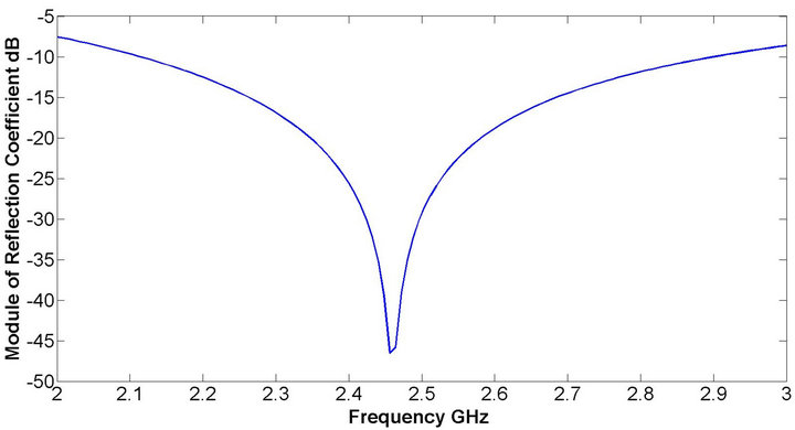
Figure 4. Simulated reflection coefficient of RAM.
rials that are able to effectively absorb and shield electromagnetic interference in a wide frequency range. In the [24] the electromagnetic shielding performance of carbon foams is accurately reported for two different type of foam GRAFOAM FPA-20 and GRAFOAM FPA-10. SEM pictures of such carbon foams are shown in Figure 5. The foam GRAFOAM FPA-10 is made of spherical cells with non-homogeneous size that pack less efficiently than tetrakaidecahedral cells. The average area of spherical interconnected pores varies in the range from 3000 µm2 to 24,000 µm2. The cell diameter varies from about 30 to 250 µm, whereas the subscale micro porosity diameter is in the range of 3 - 4 µm. Reference [24] shows that about 2 mm of FPA10 perform a shielding effectiveness of about 40 dB in the frequency band 1 - 4 GHz. GRAFOAM FPA-20 is a typical vitreous foam characterized by a periodic arrangement of open cells.
The foam is a solid structure based on cells connected through open faces.
In particular, the microstructure is formed by regular repeating of tetrahedral unit cells. The analysis of cells and pores of GRAFOAM FPA-20 founds that the length edge between two vertices of the tetrakaidecahedral cell is in the range of 350 µm to 375 µm, and the average diameter is about 350 µm [24].
Now, the FEM simulation of foams were made considering two basic cell type shape as shown in Figure 5(a) and Figure 5(b). Pore radius around 300 µm was assumed. This approximation was made in order to consider the possibility for the carbon nanotube filler of going throughout the pores of foams. In order to easier as much as possible the numerical simulation and to allow to run the simulation on a common laptop, a two dimensional FEM analysis has been computed. The computer
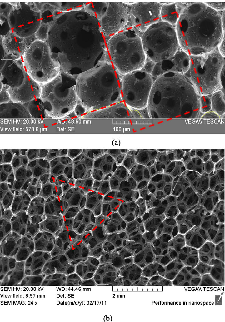
Figure 5. (a) SEM picture of GRAFOAM FPA-10. The foam exhibits a spherical microstructure with open and partly closed interconnected pores with different characteristic dimensions; (b) SEM image of carbon foam GRAFOAM FPA-20 surface with magnification of 68×. The microstructure is formed by regular 3D-arrangement of tetrahedral unit cells.
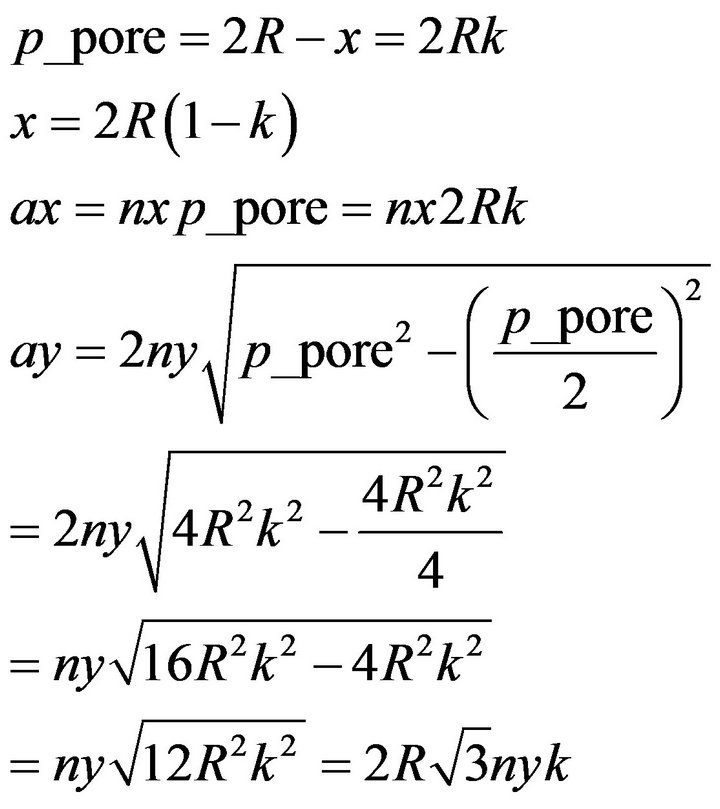
used for this simulation is a Dell M6500, and the time required for each simulation is around 15 minutes. The considerations can be extended to a three dimensional space without lack of generalities. In particular a regular array of circles connected to each other was drawn. The first model is shown in Figure 6 and described in (3). It is composed of elementary cells made by 4 circles. The parameter called k is able to model the intersection of the circles and determines the micro porosity.
The difference of the surfaces: the surface of square in blue dashed line and the surface of the four circles determines the basic cell of the foam.
Equation (3) shows the simple basic mathematical model relating the micro pores diameter and the k values. where p_pore is the step of the pores, n is the number of circles along one of the axes. The second model is shown in Figure 7 and described in (4). It is composed of ele-
 (3)
(3)
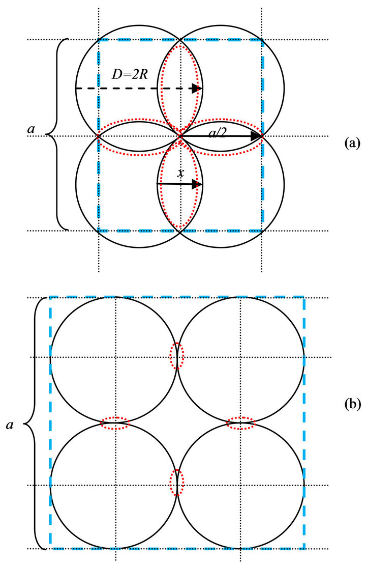
Figure 6. 2D modeling of first foam with a basic cell structure made of four adjacent pores. In (a) the micro-porosity diameter is large whilst in (b) the micro-porosity diameter is very little.
mentary cells made by 3 circles. The parameter called k is able to model the intersection of the circles and determines the micro porosity. The difference of the surfaces: the surface of triangle in blue dashed line and the surface of the three circles determines the basic cell of the foam.
In the present work the simulated foams were assumed made of graphite with an electrical conductivity of the bulk materials about 1000 S/m [10,24].
 (4)
(4)
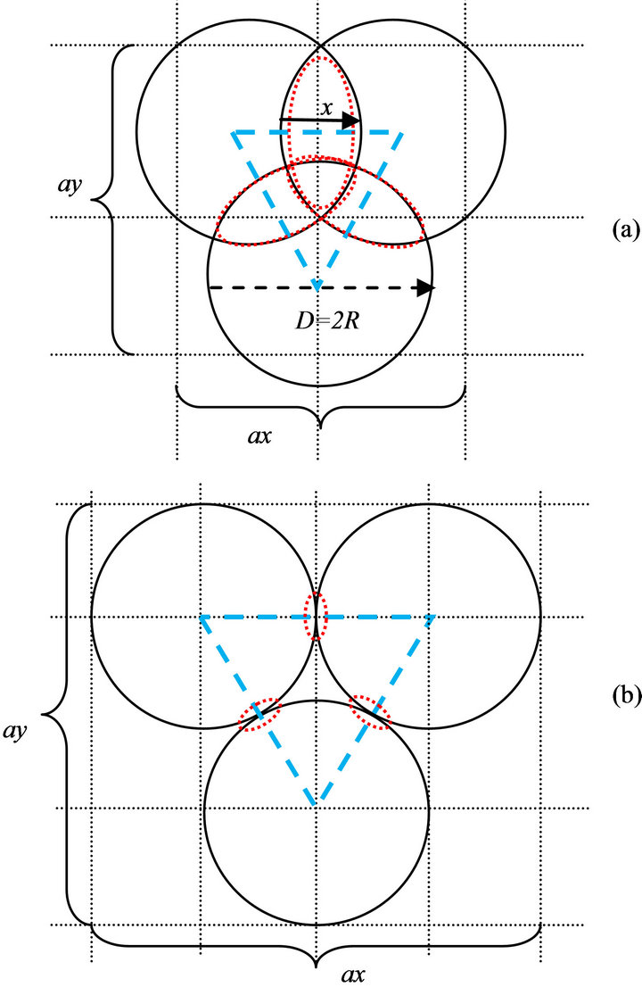
Figure 7. 2D modeling of second foam with a basic cell structure made of three adjacent pores. In (a) the microporosity diameter is large whilst in (b) the micro-porosity diameter is very little.
where p_pore is the step of the pores, nx is the number of circles along x axes and ny is the number of circles along y axes. In Figure 8, the schematic of the first type of foam absorber is shown. Here k = 0.960 and R = 300 µm. It can be noticed that foam is inserted in a closed environment where the propagation of a plane wave takes place and where a network port is provided. This port has been included in order to compute the S11 scattering parameters [15] needed to estimate the reflection coefficient of the foam. Scattering parameters or S-parameters describe the electrical behavior of linear electrical networks when undergoing various steady state stimuli by electrical signals. The module of S11, S22 is equivalent to the reflected voltage magnitude divided by the incident voltage magnitude.
Is a scalar measure of how close the actual input impedance of the single port network is to the nominal system impedance value. This parameter define the reflection of the electromagnetic field by the material at port 1. Thickness of foam is less than 1 cm.
In Figure 9, the mesh for the FEM analysis is shown. In particular the maximum dimension of the element has been assumed to be one tenth of the minimum wavelength. The Electromagnetic waves interface of COMSOL uses second order vector elements per default. This makes 10 elements per wavelength a bit overkill but this condition assure a good FEM analysis [10].
In Figure 10, the electric field is shown. It can be observed how the electric field intensity decreases in the deep part of foam evidencing the absorption mechanisms of the foam.
In Figure 11, the zoom of electric field is shown, it can be observed the intensification of the electric field around the sharp area of the foam where the interconnection between different spaces takes place.
In Figure 12, the skin-depth is plotted. The decline (i.e. attenuation) in field intensity versus depth is known as the skin effect: for high-conductivity materials the skindepth estimates the distance over which the field intensity falls to 1/e of its original value [15]. Such a property is valid for an electric conductor where the condition  is verified, while is less strong for a dielectric material (i.e. at low microwave electrical conductivity); in any case the values us give an idea of the electromagnetic behavior of the materials under test. The values obtained show that skin-depth decreases rapidly in the foam made of porous graphite where the electromagnetic field is strongly attenuated.
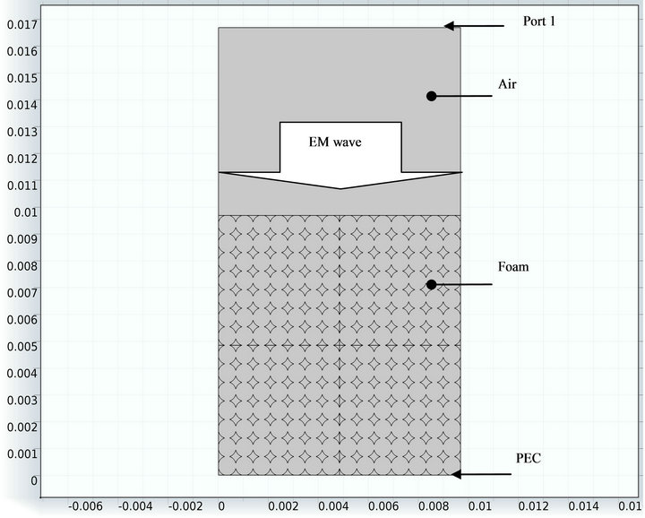
Figure 8. Scheme of the absorbing electromagnetic foam with a basic cell structure made of four adjacent pores. The material is inserted in an environment able to compute the S11 scattering parameter on the port 1 for an incident plane wave.
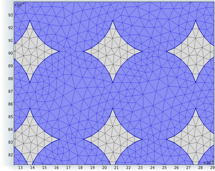
Figure 9. Mesh of the materials. Scheme of the absorbing electromagnetic foam with a basic cell structure made of four adjacent pores. The axes show the dimensions in m and the values are multiplied for 10–4.
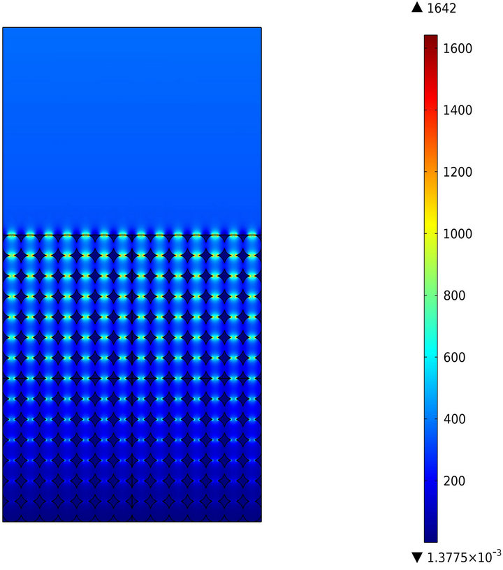
Figure 10. Electric field V/m inside the foam.
In Figure 13, are plotted the stream line of conduction current density in blue color, the arrows surface of power flow in grey color, the electric field in V/m. It can be observed that conduction current flows through the materials. In particular the intensification of the current takes place in the area of RAM made of graphite which possess an higher electrical conductivity with respect to composite materials made of epoxy-resin and MWCNT 1 wt% located inside the pores.
In Figure 14 the reflection coefficient of the RAM is shown. It can be noticed that about 9.7 mm of foam with the pores filled with MWCNT shows a minimum value of the reflection coefficient of −17 dB around 2.4 GHz i.e. around the center of frequency band. The dielectric properties of MWCNT 1 wt% are shown in Figure 2.
In Figures 15 and 16, the schematic and the mesh of the second type of foam absorber is shown. Now k = 0.997 and R = 300 µm.
The structure in Figures 15 and 16, shows quite well the dimensions of the pores and the. This time the morphology is different and each single pore have 6 connection with the 6 surrounding pores. The three-dimensional version of this morphology is the tetrakaidecahedral cell. In Figures 17 and 18 the electric field in V/m and the skin-depth in m are shown.
In Figure 19, the stream line of conduction current
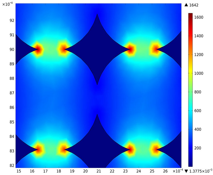
Figure 11. Zoom of electric field V/m.
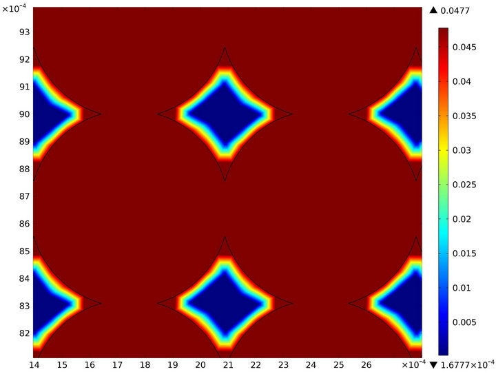
Figure 12. Zoom of skin-depth m.
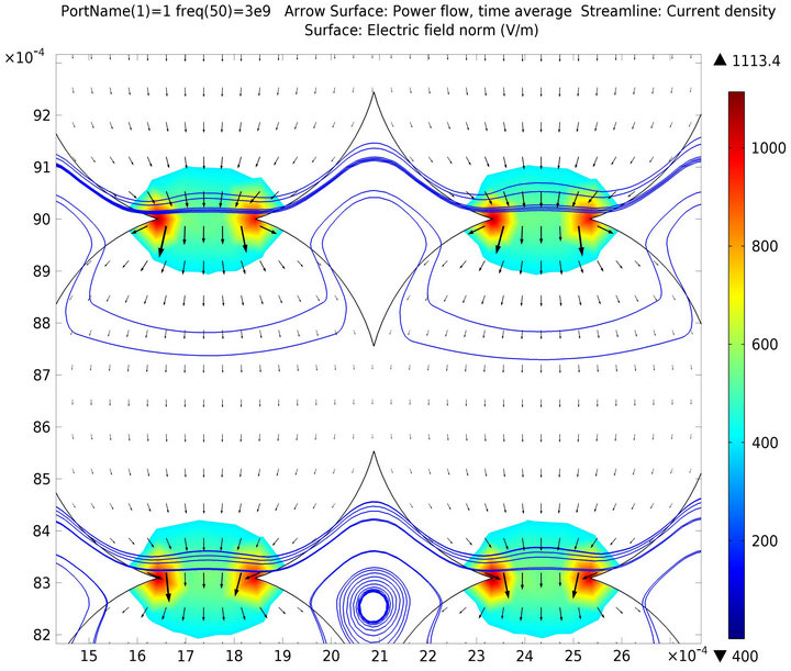
Figure 13. Stream line of conduction current density in blue color, the arrows surface of power flow in grey color, the electric field in V/m.
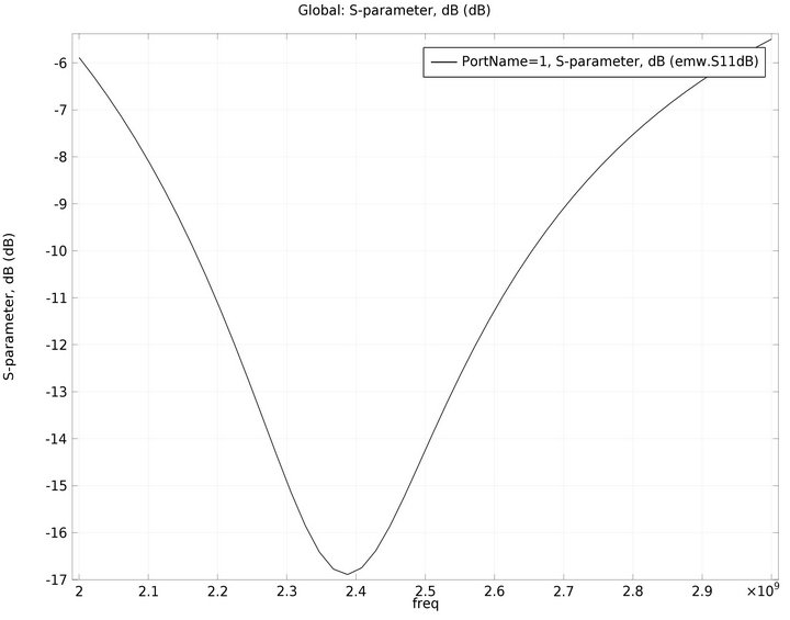
Figure 14. Reflection coefficient dB of first type of foam. Frequency is in Hz.
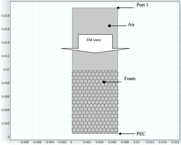
Figure 15. Scheme of the absorbing electromagnetic foam with a basic cell structure made of three adjacent pores. The material is inserted in an environment able to compute the S11 scattering parameter on the port 1 for an incident plane wave. Axes report the dimension in m.

Figure 16. Mesh of the materials. Scheme of the absorbing electromagnetic foam with a basic cell structure made of three adjacent pores. The axes show the dimensions in m and the values are multiplied for 10–4.

Figure 17. Zoom of electric field V/m.
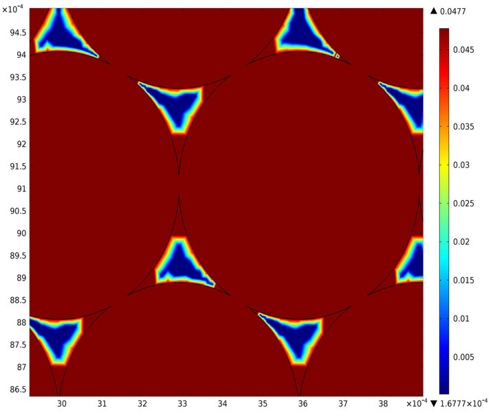
Figure 18. Zoom of skin-depth m.
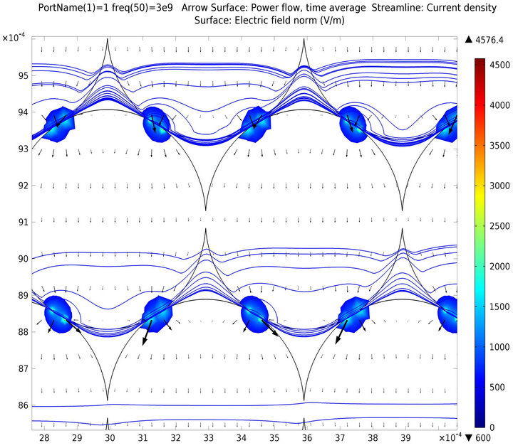
Figure 19. Stream line of conduction current density in blue color, the arrows surface of power flow in grey color, the electric field in V/m.
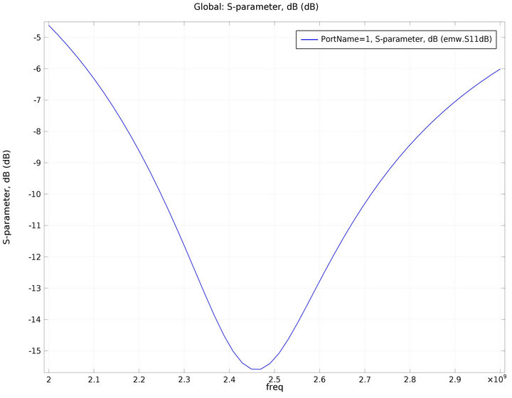
Figure 20. Reflection coefficient dB of second foam. Frequency is in Hz.
density in blue color, the arrows surface of power flow and in grey color, the electric field in V/m are shown. It can be observed how the flux lines of the current density are more concentrated within the graphite materials having higher electrical conduction with respect to the dielectric made of epoxy-resin and MWCNT 1 wt%. In Figure 20 the reflection coefficient of the RAM is shown. It can be noticed that about 9.7 mm of foam with the pores filled with MWCNT shows a minimum value of the reflection coefficient of –16 dB around 2.45 GHz i.e. around the center of frequency band.
6. Conclusions
In this paper the absorption of the electromagnetic field in the frequency range of 2 GHz - 3 GHz has been analyzed by using carbon foams and carbon nanotubes. Two different kind of materials have been taken into account and both shows an interesting behavior of the reflection coefficient which reach values between –17 dB and –45 dB around the center of frequency band. It looks like that the material made of carbon nanotubes works much better than carbon foams.
This study shows that this materials could be effectively taken into consideration for a future application in the mitigation of human exposure to electromagnetic fields and for all the applications where absorption of electromagnetic fields is required.
REFERENCES
- “Statement on the ‘Guidelines for Limiting Exposure to Time-Varying Electric, Magnetic and Electromagnetic Fields (up to 300 GHz)’,” International Commission on Non-Ionizing Radiation Protection (ICNIRP), 2009.
- “IEEE Standard for Safety Levels with Respect to Human Exposure to Radio Frequency Electromagnetic Fields, 3 kHz to 300 GHz,” Institute of Electrical and Electronics Engineers (IEEE), IEEE Std C95.1, 2005.
- World Health Organization, “Base Stations & Wireless Networks, Exposures & Health Consequences,” World Health Organization, Geneva, 15-16 June 2005.
- “Electromagnetic Fields and Public Health,” Mobile Phones Fact Sheet No 193, June 2011.
- D. Micheli, R. Pastore, C. Apollo, M. Marchetti, G. Gradoni, V. M. Primiani and F. Moglie, “Broadband Electromagnetic Absorbers Using Carbon Nanomaterial-Based Composites,” IEEE Transaction on Microwave and Techniques, Vol. 59, No. 10, 2011, pp. 2633-2646. doi:10.1109/TMTT.2011.2160198
- D. Micheli, C. Apollo, R. Pastore, D. Barbera, R. B. Morles, M. Marchetti, G. Gradoni, V. M. Primiani and F. Moglie, “Optimization of Multilayer Shields Made of Composite Nanomateriald Materials,” IEEE Transaction on Electromagnetic Compatibility, Vol. 54, No. 1, 2012, pp. 60-69. doi:10.1109/TEMC.2011.2171688
- D. Micheli, R. Pastore and M. Marchetti, “Modeling of Radar Absorbing Materials Using Winning Particle Optimization Applied on Electrically Conductive Nanostructured Composite Material,” The International Journal of Material Science, 2012, in press.
- Z. Fang, X. Cao, C. Li, H. Zhang, J. Zhang and H. Zhang, “Investigation of Carbon Foams as Microwave Absorber: Numerical Prediction and Experimental Validation,” Elsevier, Carbon, Vol. 44, No. 15, 2006, pp. 3368-3370. doi:10.1016/j.carbon.2006.07.014.
- Z. Fang and C. Fang, “Novel Radar Absorbing Materials with Broad Absorbing Band: Carbon Foams,” Applied Mechanics and Materials, Vol. 26, No. 28, 2010, pp. 246- 249. doi:10.4028/www.scientific.net/AMM.26-28.246.
- “Multiphysics Modeling, Finite Element Analysis, and Engineering Simulation Software.” http://www.comsol.com
- H. Xua, H. Abe, M. Naito, Y. Fukumori, H. Ichikawa, S. Endoh and K. Hata, “Efficient Dispersing and Shortening of Super-Growth Carbon Nanotubes by Ultrasonic Treatment with Ceramic Balls and Surfactants,” Elsevier, Advanced Powder Technology, Vol. 21, No. 5, 2010, pp. 551-555. doi:10.1016/j.bbr.2011.03.031
- A. M. Nicolson and G. F. Ross, “Measurement of the Intrinsic Properties of Materials by Time-Domain Techniques,” IEEE Transactions on Instrumentation and Measurement, Vol. IM-19, No. 4, 1970, pp. 377-382. doi:10.1109/TIM.1970.4313932
- J. Baker-Jarvis, “Transmission/Reflection and Short-Circuit Line Permittivity Measurements,” US Department Commerce, NIST, Washington DC, 1990.
- A.-H. Boughriet, C. Legrand and A. Chapoton, “Noniterative Stable Transmission/Reflection Method for LowLoss Material Complex Permittivity Determination,” IEEE Transactions on Microwave Theory and Techniques, Vol. 45, No. 1, 1997, pp. 52-57. doi:10.1109/22.552032
- S. Ramo, J. R. Whinnery and T. Van Duzer, “Fields and Waves in Communication Eletronics,” John Whiley & Sons, Hoboken, 1994.
- Y. Huanga, N. Lia, Y. F. Ma, F. Du, F. F. Lin, X. B. He, X. Lin, H. J. Gao and Y. S. Chen, “The Influence of Single-Walled Carbon Nanotube Material on the Electromagnetic Interference Shielding Efficiency of Its Epoxy Composites,” Elsevier, Carbon, Vol. 45, No. 8, 2007, pp. 1614-1621. doi:10.1016/j.carbon.2007.04.016
- N. Li, Y. Huang, F. Du, X. He, X. Lin, H. Gao, Y. Ma, F. Li, Y. Chen and P. C. Eklund, “Electromagnetic Interference (EMI) Shielding of Single-Walled Carbon Nanotube Epoxy Composites,” Nano Letters, Vol. 6, No. 6, 2006, pp. 1141-1145. doi:10.1021/nl0602589
- “Introduction to Solid State Physics,” 6th Edition, John Whiley & Sons, New York, 1986, pp. 448-456.
- D. Micheli, C. Apollo, R. Pastore and M. Marchetti, “XBand Microwave Characterization of Carbon-Based Nanocomposite Material, Absorption Capability Comparison and RAS Design Simulation,” Composites Science and Technology, Elsevier, Vol. 70, No. 2, 2010, pp. 400-409. doi:10.1016/j.compscitech.2009.11.015
- S. Begley, “Electromagnetic Properties of Materials: Characterization at Microwave Frequencies and Beyond,” Application Development Engineer Agilent Technologies, 2009.
- Application Note, “Basics of Measuring the Dielectric Properties of Materials,” Agilent Technologies, 2000. http://cp.literature.agilent.com/litweb/pdf/5989-2589EN.pdf
- D. Micheli, “Radar Absorbing Materials and Microwave Shielding Structures Design,” LAP Lambert Academic Publishing, Saarbrücken, 2012, 476 p.
- L. J. Gibson and M. F. Ashby, “Cellular Solids: Structure and Properties,” 2nd Edition, Cambridge University Press, Cambridge, 1997.
- F. Moglie, D. Micheli, S. Laurenzi, M. Marchetti and V. P. Mariani, “Electromagnetic Shielding Performance of Carbon Foams,” Carbon, Vol. 50, No. 5, 2012, pp. 1972- 1980. doi: 10.1016/j.carbon.2011.12.053