Materials Sciences and Applications
Vol.3 No.10(2012), Article ID:23496,10 pages DOI:10.4236/msa.2012.310099
Ab Initio Calculations Study of Structural and Electronic Properties of Ternary Alloy AlxIn1–xAs
![]()
Physics Department, Faculty of Science, Djillali Liabes University, Sidi Bel Abbes, Algeria.
Email: *lttnsameri@yahoo.fr
Received July 17th, 2012; revised August 20th, 2012; accepted September 16th, 2012
Keywords: FP-LMTO; DFT; Arsenide Compounds; Band Gap Bowing; Effective Masses
ABSTRACT
First principles calculations of the structural and electronic properties of AlAs, InAs and their alloy AlxIn1−xAs have been performed using the full-potential linear muffin-tin orbital (FP-LMTO) [1] method within density functional theory (DFT) [2,3]. We used the local density approximation (LDA) [4] within the generalized gradient correction (GGA) [5] to calculate the electronic structure at equilibrium volume. The effect of composition on lattice constants, bulk modulus and band gap were investigated. Deviations of the lattice constants from Vegard’s law and the bulk modulus were observed for this alloy. The microscopic origins of the gap bowing were explained by using the approach of Zunger and co-workers [6-9].
1. Introduction
The III-V group compounds XAs (X = Al, Ga and In) with binary octets of ANB8−N type have drawn profound attention recently, because of their scientific applications in fabricating heterostructures and tunable devices in the visible wavelength region, optoelectronic devices, explicitly in the high frequency range, etc. [10]. The performance of the devices strongly depends on the inherent thermodynamic and transport properties of these compounds, for example, the dielectric constants and phonon frequencies. Kamioka et al. [11] and Lockwood et al. [12] determined experimentally the dielectric constants and phonon frequencies for zinc blende type XAs at normal conditions. The band structure and density of state (DOS) of XAs have been studied and discussed by theoretical investigations [13-18]. The dielectric function also has been investigated corresponding to the band gap transition for AlAs [18,19]. Moreover, a number of experimental and theoretical studies on the lattice dynamical characteristics have been carried out, including some on the vibrational properties of the XAs alloys [10-19].
The semiconductors (BAs, AlAs, GaAs and InAs) are important materials in the fields of fabrication of microwaves, optoelectronic, and electronic devices; they provide a good basis for many established commercial and new technological applications such as light emitting diodes, lasers, integrated circuits, modulators, photodetectors and filters [20]. III .arsenide compounds belong to a family of common-anion III-V semiconductors.
They have the widest range of energy gaps apart from III-nitrides and under normal conditions; these materials crystallize in the zinc blende structure [21]. Aluminum arsenide (AlAs) is indirect band gap semiconductor; it’s one of the most important electronic and optoelectronic materials because of its frequent incorporation into GaAs-based hetero-structures [21,22]. While Indium arsenide (InAs) is a direct band gap semiconductor, it’s used for construction of infrared detectors, for the wavelength range of 1 - 3.8 µm. The detectors are usually photovoltaic photodiodes. Cryogenically cooled detectors have lower noise, but InAs detectors can be used in higher-power applications at room temperatures as well. Indium arsenide is also used for making of diode lasers. AlAs, GaAs and InAs are fundamentals to a wide variety of optoelectronic hetero-junction systems. This includes short period super-lattice and
and  [23], bulk alloys such as AlxIn1–xAs and InxGa1–xAs [24]. InAs is well known for its high electron mobility and narrow energy band gap. It’s widely used as terahertz radiation source as it is a strong photo-Dember emitter [25].
Aluminum indium arsenide is a semiconductor material with very nearly the same lattice constant as GaInAs; but a larger band gap is used as a buffer layer in metamorphic HEMT transistors, it can be also used to form alternate layers with GaInAs, which act as quantum wells; these structures are used in broad band quantum cascade lasers. The toxicology of AlInAs has not been fully investigated; the dust is an irritant to skin, eyes and lungs. The environment, health and safety aspects of AlxIn1–x As (such as trimethylindium and arsine) and industrial hygiene monitoring studies of standard MOVPE sources have been reported in a review [26].
2. Computational Details
Electronic configurations are: Al: Ne3s23p1; As: Ne3d10 4s24p3 and In: Kr4d105s25p1. Atoms in zinc blende structure are in FCC positions as X (0, 0, 0); As (1/4, 1/4, 1/4) where X (=Al, In). In order to compute equilibrium structural parameters and electronic band structure of AlAs, InAs and their ternary alloy AlxIn1–xAs, we have employed the available Lmtart code [27]. This includes full potential linearised muffin-tin orbitals (FP-LMTO) method [1] within the density functional theory (DFT) [2,3] by using the local density approach (LDA) [4] and the gradient generalized approach (GGA) [5]. The FPLMTO method treats muffin-tin spheres (MTs) and interstitial regions (IRs) on the same footing, leading to best precision of the eigenvalues. At the same time, the FP-LMTO method, in which the space is divided into an IR and non-overlapping (MT) spheres surrounding the atomic sites, uses a more complete basis than its predecessors. In the IR regions, the basic functions are represented by Fourier series. Inside the MT spheres, the basic functions are expanded in combinations of spherical harmonics functions. A short description of this method can be found in Ref. [28]. The values of the sphere radii (MTs) and the number of plane waves (NPLW) used in our calculations are listed in Table 1.
We have made an application on unit cells containing eight atoms in order to stimulate x = 0.25; 0.50 and 0.75 by substituting In atoms by Al atoms in the cation sublattice of ZB phases.
3. Results and Discussion
3.1. Structural Properties
To test the reliability of the ab initio method and the simulated results, determinations of the lattice parameters of binary compounds AlAs and InAs have been done by minimization of the total energy, than a best fitting by using the Murnaghan equation of state [29]. Our results are given in the Table 2 (in a.u.) and there are in well agreement with those obtained experimentally. We note that the LDA underestimated the lattice parameters and overestimated the bulk modulus while the GGA overestimated the lattice parameters.
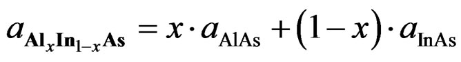
The lattice parameters (a) of ternary alloy can be expressed as a linear combination of the lattice constants of the two forming binary alloys, the physical properties of ternary alloy are usually investigated based on Vegard’s law [30,31]:
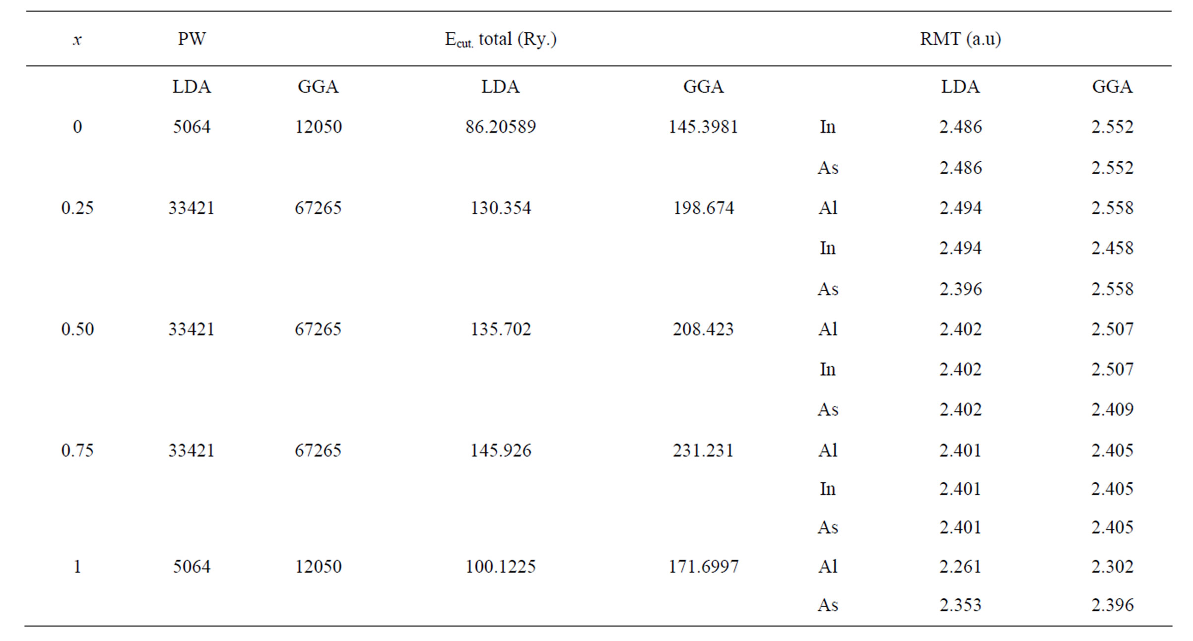
Table 1. The plane wave number PW, energy cutoff (in Ry) and muffin-tin radius (RMT) (in a.u) used in calculation for binary InAs, AlAs and their ternary AlxIn1–xAs alloy in zinc-blende (ZB) structure.
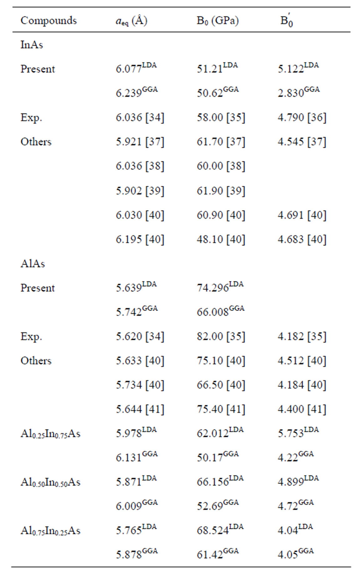
Table 2. The structural properties (lattice parameter a, bulk modulus B and its pressure derivative B' for AlAs, InAs and their ternary alloy.
 (1)
(1)
where, aAlAs, aInAs and  are, respectively, the lattice constant of the compounds AlAs, InAs and AlxIn1–xAs. In Figures 1 and 2, we present a comparison between results obtained for the calculated lattice parameters and the bulk modulus and those obtained from Vegard’s law, that correspond to the zinc blende configuration of the ternary alloy AlxIn1–x As at different concentration x. In Figure 1 we show that the lattice constant (a) of the ternary alloy decreases with an increase in Al concentration, in the both approximations LDA and GGA. The lattice parameters scale linearly with concentration thus obeying Vegard’s law [30,31]. Our results show a marginal upward bowing parameters equal to −0.06057 Å and 1.06171 Å with both approximations LDA and GGA respectively. It’s clear that this phenomenon occurs because the atom of Aluminum (Al)
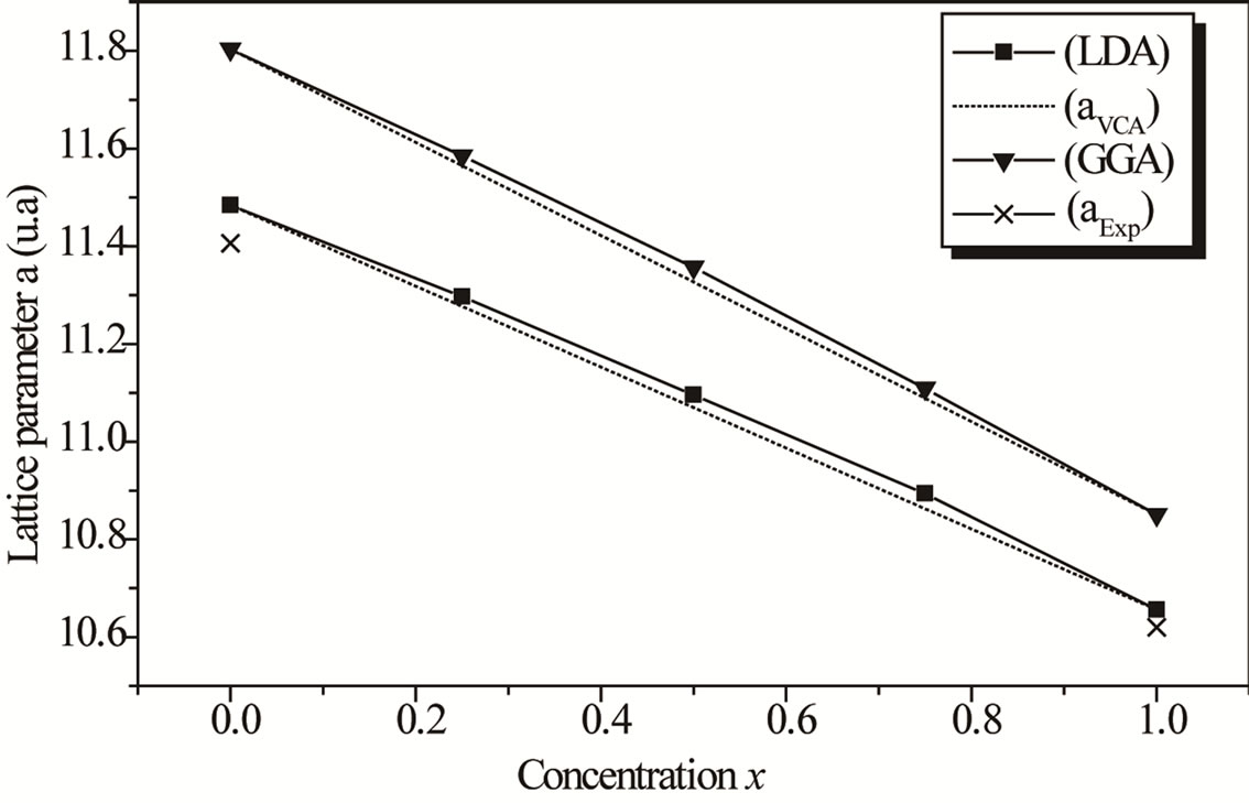
Figure 1. Composition dependence of the calculated lattice parameters within GGA (down triangle) and LDA (solid square) of AlxIn1–xAs alloy compared with Vegard’s prediction (dot line).
 (a)
(a)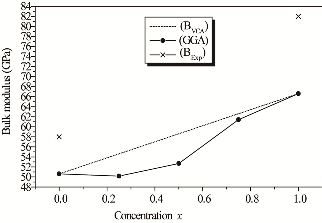 (b)
(b)
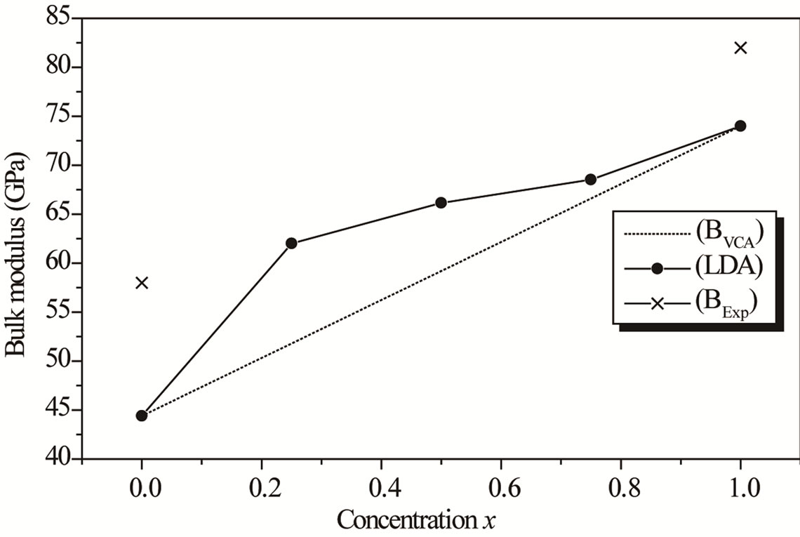
Figure 2. Composition dependence of the calculated bulk modulus within LDA (Solid square) (a) and GGA (Up Triangle) (b) of AlxIn1−xAs alloy compared with Vegard’s prediction.
is smaller than that of Indium (In). Hence, the lattice parameter can be written as
 (2)
(2)
where the quadratic term b is the bowing parameter. In Figures 2(a) and (b), we observe that the bulk modulus increases with Al concentration. A large deviation of the bulk modulus from the linear concentration dependence (LCD) with an upward bowing parameter equal to –13.52686 GPa by using the LDA approximation; while the GGA approximation gave downward value of 18.61257 GPa. The deviation from LCD should be mainly due to the bulk modulus mismatch between AlAs and InAs compounds. A more precise comparison for the behavior of the AlxIn1–xAs ternary alloy shows that a decrease of the lattice constant is accompanied by an increase of the bulk modulus. It represents bond strengthening or weakening effect induced by changing the concentration.
3.2. Electronic Properties
The calculated band structure energies of binary compounds as well as their alloy by using the FP-LMTO method within both the local density approximation (LDA) and the generalized gradient correction (GGA) exhibit an indirect gap at X point for AlAs and a direct gap at Γ point for InAs. There is an indirect gap at R point in the ternary alloy with GGA for which the band gap energy in Figure 3.
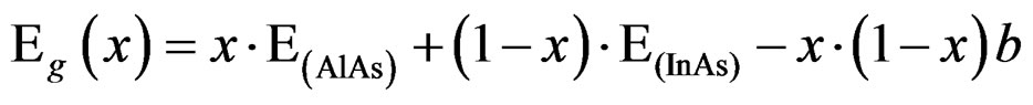
The band gap energy of AlxIn1−xAs can be depicted as a function of the aluminum composition x, and be expressed by using the following formula:
 (3)
(3)
where Eg(x) denotes the band gap energy of AlxIn1–xAs, and Eg(AlAs) and Eg(InAs) denote the band gap energy of AlAs and InAs, respectively, and b is the band gap bowing parameter of AlxIn1–xAs.
Our results are given in Table 3. It is well known that the GGA and LDA usually underestimated the energy gap [32]. We note that a calculation of the band gap for our basic semiconductor InAs gives the result Eg = 0.00 eV which seems to be smaller than the literature values, and the same for the AlAs semiconductor, this is due to the well-known and systematical underestimation of DFT in GGA and LDA approaches. Note that this band gap underestimation doesn’t affect the conclusions made.
 (4)
(4)
 (5)
(5)
 (6)
(6)
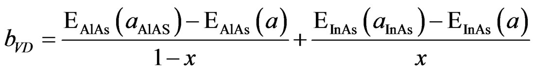
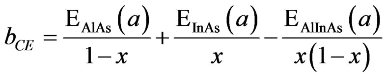
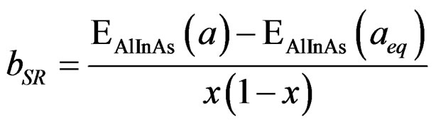
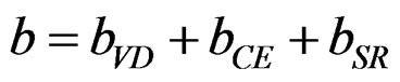
In order to derive a phenomenological model for computing the band gap bowing (b), we decompose b into three physically distinct contributions [33]; 1) volume deformation (VD); 2) charge exchange (CE); and 3) structural relaxation (SR). The (VD) term represented the relative response of the binary compounds (AlAs) and (InAs) to the hydrostatic pressure from their individual equilibrium lattice constant to the alloy value a(x). The second contribution, the charge exchange (CE) is related to a charge transfer in bringing (AlAs) and (InAs) at a = a(x). Finally, the (SR) term described the charge in the band gap upon passing from the unrelaxed to the relaxed alloy, i.e., a(x) → a(eq.) by construction the total bowing (b) which is given in Equation (7):
 (7)
(7)
The calculated total optical band gap bowing (b) and its three contributions (bVD, bCE and bSR) are given in Table 4, we note that from x = 0.25 to 0.75, the main contribution to the gap bowing raises from the VD effect, whereas, for x = 0.75, the contribution of SR is increase. Figure 4 shows the variation of the band gap bowing versus concentration. The bowing remains linear and varies slowly for x = 0.50, it decreases faster which checked the evaluation of the parameters of constants and the gap according to concentration: the calculated gap bowing parameter coefficient b for the ternary alloy ranges from 1.97 eV (x = 0.25) to 0.73 eV (x = 0.75) for the GGA and from 1.81 eV (x = 0.25) to 0.59 eV (x = 0.75) for the LDA.
3.3. Effective Masses
An effective mass is an important material parameter describing most of carrier transport properties in semiconductors [49,50]. Its importance becomes recently even greater as the technology of optoelectronic devices matures and its precise knowledge becomes critical. Its values, however, known from scientific literature for a given semiconductor material, differ usually considerably from one another. The knowledge of effective masses of electrons and holes is important for the excitonic properties of the investigated compounds. Experimentally, the effective masses are usually determined by cyclotron resonance, electro reflectance measurements or from analysis of transport data or transport measurements [51]. Theoretically, the effective masses can be estimated from the energy band curvatures. Generally, the effective mass is a tensor with nine components, however for the much idealized simple case, where the E(k) diagram can be fitted by a parabola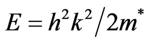 , the effective mass becomes a scalar at high symmetry point in the Brillouin zone. Therefore, we have calculated the effective mass of electrons and holes using GGA scheme. We have computed the electron effective mass at the conduction
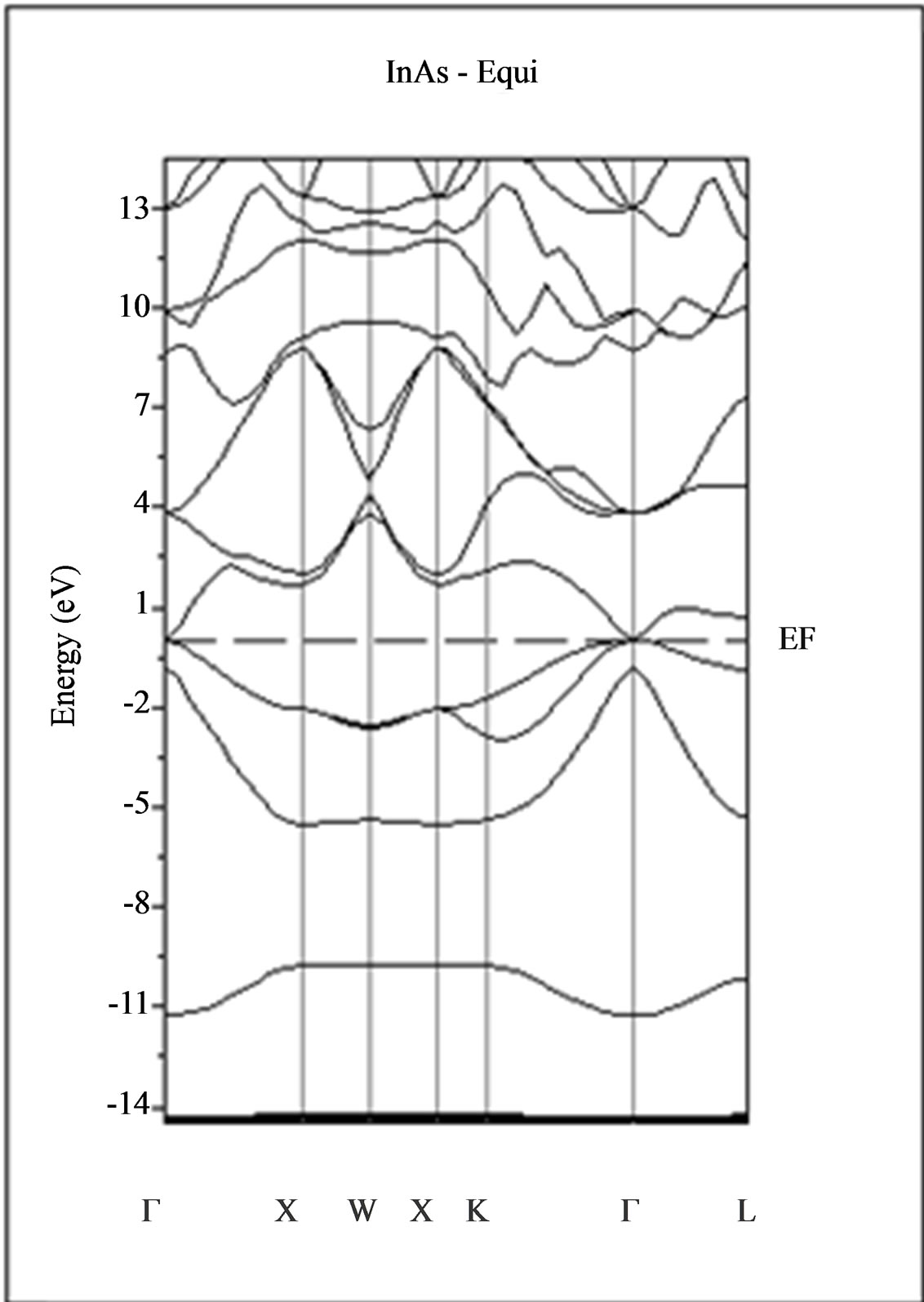
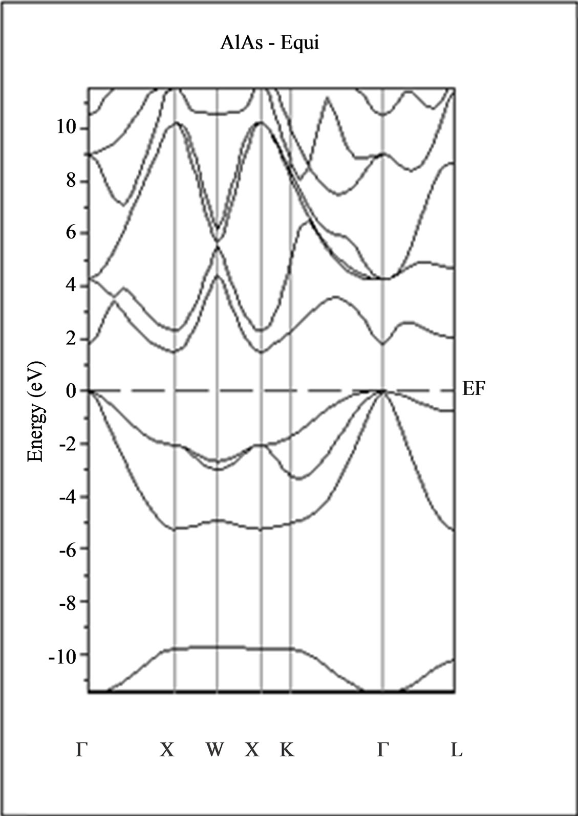
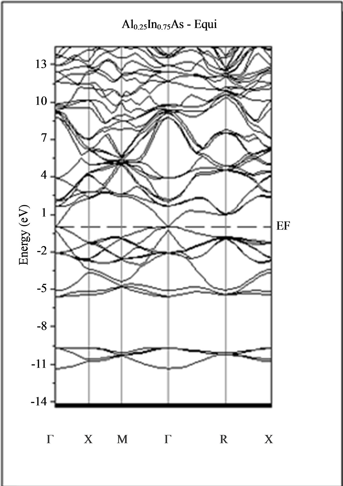
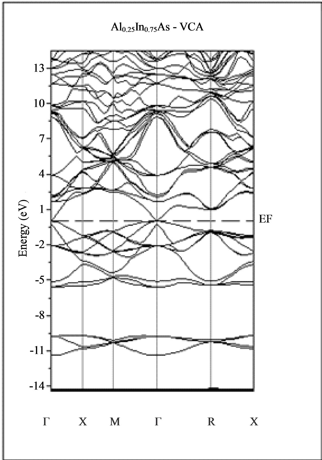

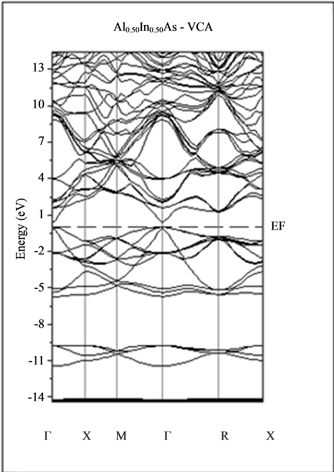
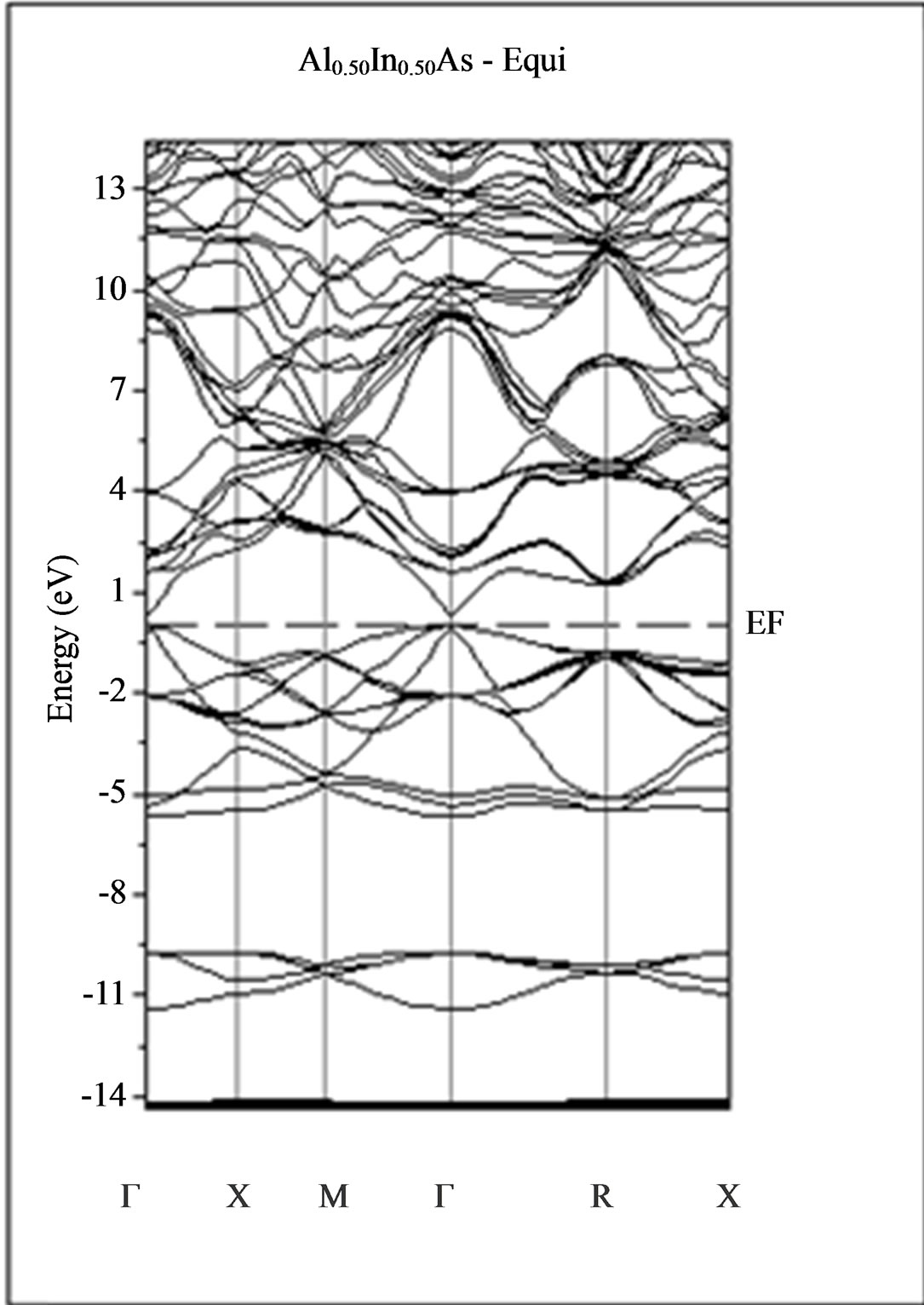
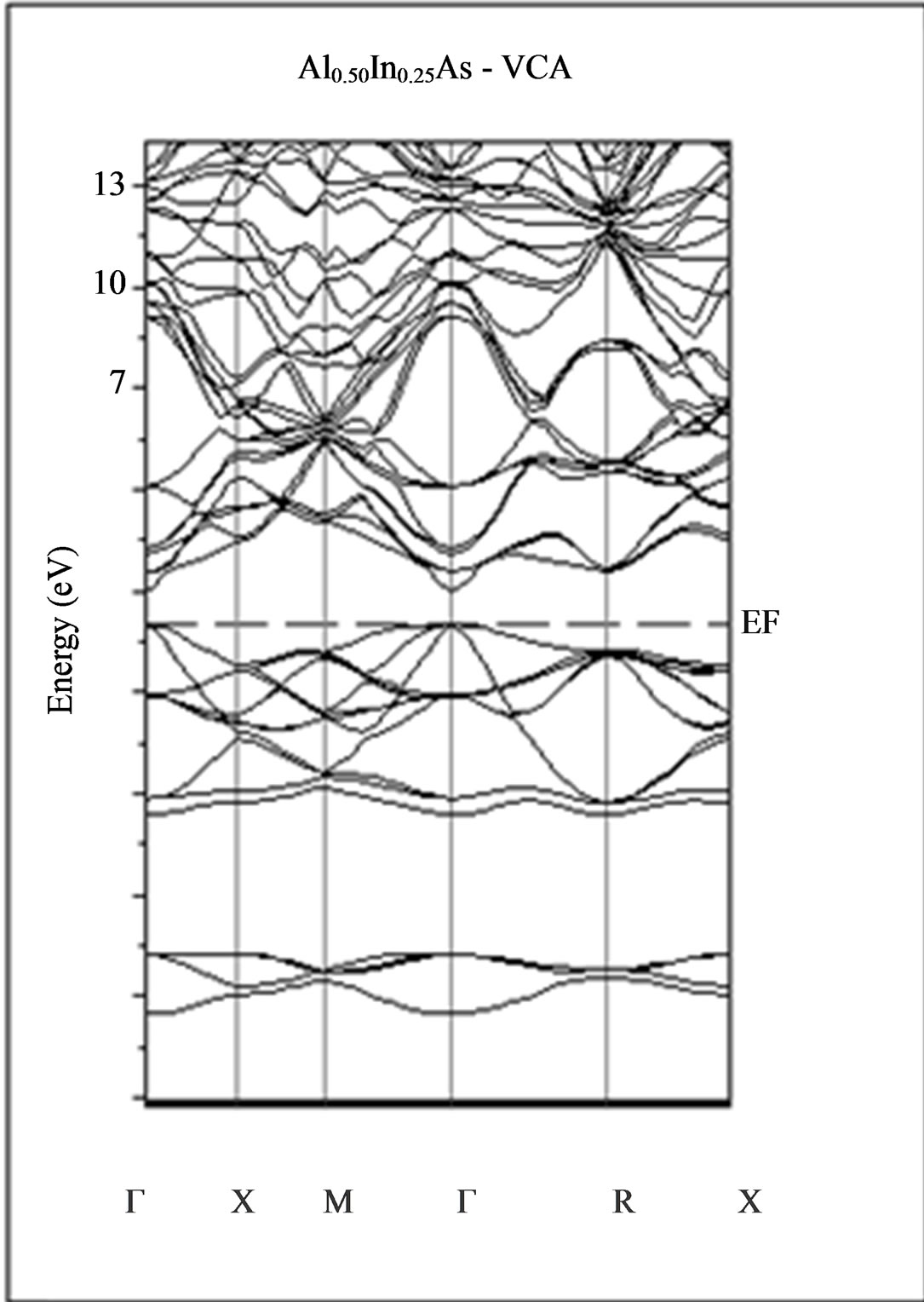
Figure 3. Band structures of zinc blende for AlAs, InAs and AlxIn1–xAs along the principle high symmetry directions in the Brillouin zone with GGA.

Table 3. The energy band gap (Eg) of AlAs, InAs and their ternary alloy AlxIn1–xAs.
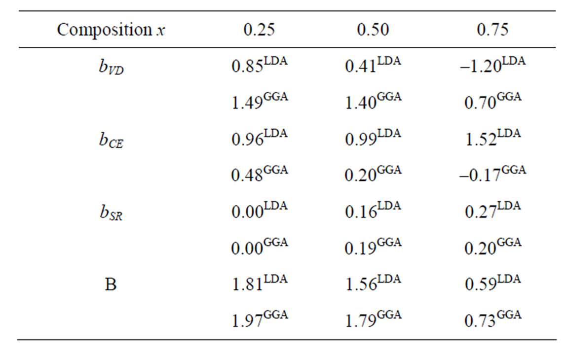
Table 4. Decomposition of optical bowing into volume deformation (VD), charge exchange (CE) and structural relaxation (SR) contributions for AlxIn1–xAs alloy (in eV).
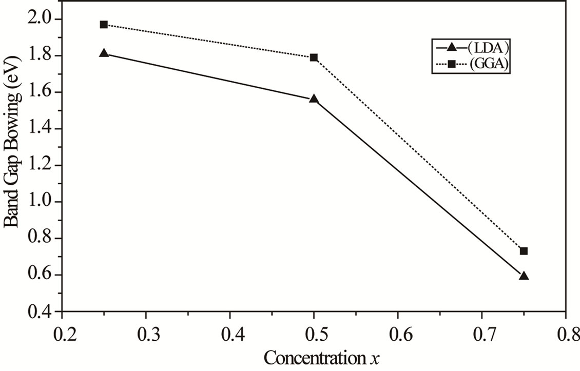
Figure 4. The calculated band gap bowing parameter in LDA (up triangle) and GGA (solid square) as a function of concentration x.
band minima (CBM) and the hole effective mass at the valence band maxima (VBM) for the composition ranging from 0 to 1 for AlxIn1−xAs. We have computed the electron effective mass at the conduction band minima (CBM) and the hole effective mass at the valence band maxima (VBM) for the composition ranging from 0 to 1 for AlxIn1–xAs alloys. The electron effective mass value is obtained from the curvature of the conduction band near the X-point for AlAs and near the Γ-point at the CBM from X = 0 to 0.75. The hole effective mass value is calculated from the curvature near the Γ-point at the VBM for all concentration. From Table 5, it is worth mentioning that the hole (heavy and light) effective masses are strongly varied from composition to another. This could be attributed to the change of the position of the conduction band minimum (CBM). Table 5, gives our present values of effective masses (electron, heavy hole and light hole) for the ternary alloy AlxIn1–xAs at the Г point of the Brillouin zone at various compositions, except for x = 1, where we calculated effective masses at X point of the Brillouin zone. Our results concerning the electrons and holes are displayed in Figure 5. Our calculated effective masses for AlAs and InAs are found comparable to those others theoretical values. To the best of our knowledge, there are no earlier data on the effective masses of the studied alloy at 0.25, 0.5 and 0.75; we feel that our calculations can be used to cover the lack of data in the literature for this alloy.
4. Conclusion
In summary, we have performed ab initio calculations
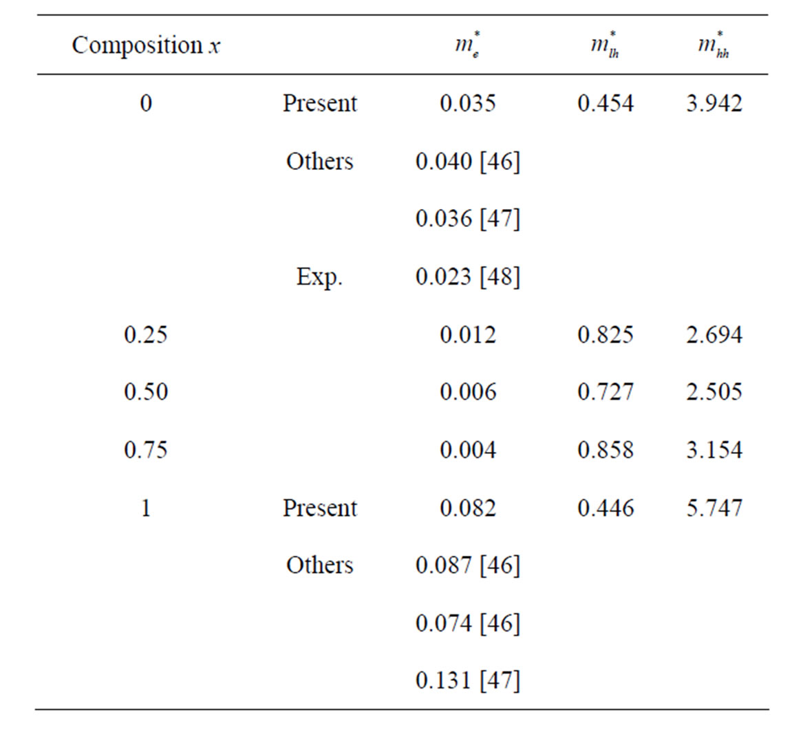
Table 5. Electron ( ), light hole (
 ) and heavy hole (
 ) effective masses (in units of free electron mass m0) of the ternary alloy AlxIn1–xAs using LDA and GGA.
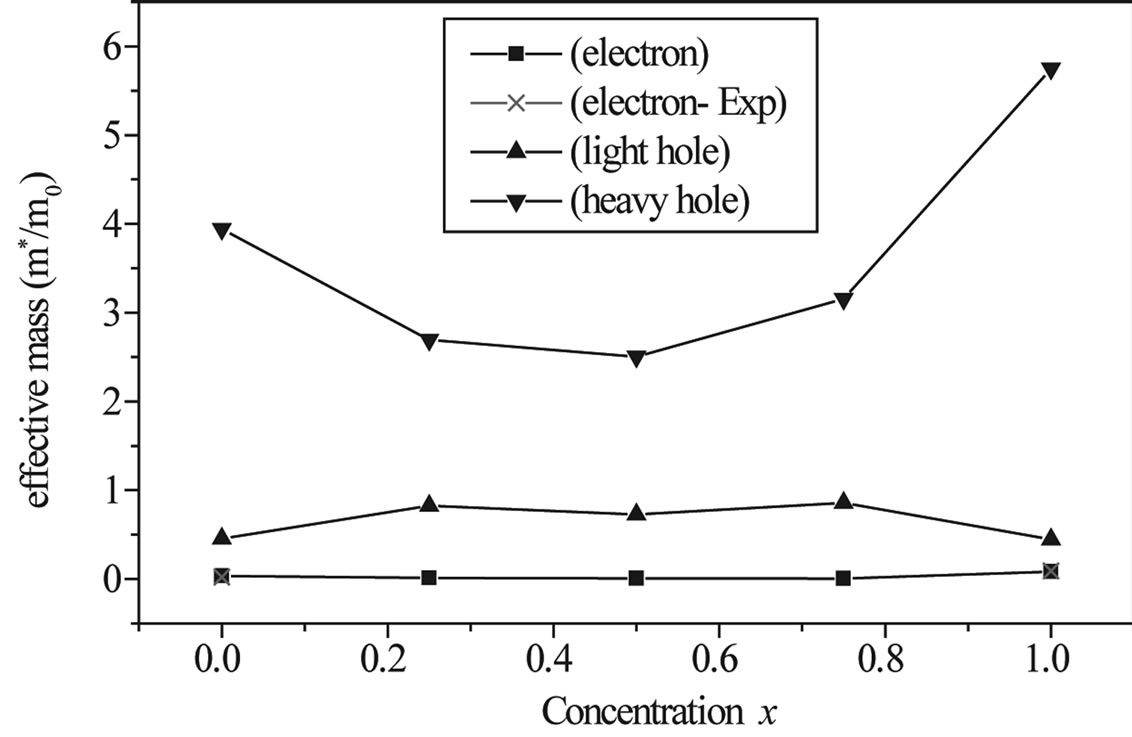
Figure 5. The effective mass (in units of free electron mass m0) of Al composition for electron (solid square) heavy hole (down triangle) and light hole (up triangle).
using the full-potential linearised muffin-tin orbitals (FP-LMTO) method in conjunction with both the LDA and GGA approximations for exchange-correlation potential to investigate the structural and electronic properties of the zinc blende AlxIn1–xAs alloy. We have calculated the concentration dependence of the lattice parameter, the bulk modulus, the band gap, bowing gap and effective masses. A linearity following the Vegard’s law with lattice parameter has been shown, but we showed a large deviation from Vegard’s law with bulk modulus. In addition, we have computed the effective masses of electron and holes. Our results provide an estimate of this important compound.
REFERENCES
- S. Y. Savrasov and D. Y. Savrasov, “Full-Potential LinearMuffin-Tin Orbital Method for Calculating Total Energies and Forces,” Physical Review B, Vol. 46, No. 19, 1992, pp. 12181-12195. doi:10.1103/PhysRevB.46.12181
- P. Hohenberg and W. Kohn, “Inhomogeneous Electron Gas,” Physical Review, Vol. 136, No. 3B, 1964, pp. B864-B871. doi:10.1103/PhysRev.136.B864
- W. Kohn and L. J. Sham, “Self-Consistent Equations Including Exchange and Correlation Effects,” Physical Review A, Vol. 140, No. 4A, 1965, pp. A1133-A1138. doi:10.1103/PhysRev.140.A1133
- J. P. Perdew and Y. Wang, “Accurate and Simple Analytic Representation of the Electron-Gas Correlation Energy,” Physical Review B, Vol. 45, No. 13, 1992, pp. 13244-13249. doi:10.1103/PhysRevB.45.13244
- J. P. Perdew, S. Burke and M. Ernzerhof, “Generalized Gradient Approximation Made Simple,” Physical Review Letters, Vol. 77, No. 18, 1996, pp. 3865-3868. doi:10.1103/PhysRevLett.77.3865
- S.-H. Wei, L. G. Ferreira, J. E. Bernard and A. Zunger, “Electronic Properties of Random Alloy: Special QuasiRandom Structures,” Physical Review B, Vol. 42, No. 15, 1990, pp. 9622-9649. doi:10.1103/PhysRevB.42.9622
- S.-H. Wei and A. Zunger, “Disorder Effects on the Density of States of the II-VI Semiconductor Alloy HgCdTe, ZnCdTe and HgZnTe,” Physical Review B, Vol. 43, No. 2, 1991, pp. 1662-1677. doi:10.1103/PhysRevB.43.1662
- J. E. Bernard and A. Zunger, “Optical Bowing in Zinc Chalcogenide Semiconductor Alloy,” Physical Review B, Vol. 34, No. 8, 1986, pp. 5992-5995. doi:10.1103/PhysRevB.34.5992
- G. P. Srivastava, G. L. Martins and A. Zunger, “Atomic Structure and Ordering in Semiconductor Alloys,” Physical Review B: Rapid Communications, Vol. 31, 1985, pp. 2561-2564.
- D. C. Gupta and S. Kulshrestha, “Effect of High Pressure on Polymorphic Phase Transition and Electronic Structure of XAs (X = Al, Ga, In),” Phase Transitions: A Multinational Journal, Vol. 82, No. 12, 2009, pp. 850-865. doi:10.1080/01411590903326628
- H. Kamioka, S. Saito and T. Suemoto, “Observation of Coherent Plasmon-Phonon Coupled Mode in InAs,” Journal of Luminescence, Vol. 87-89, 2000, pp. 923-926. doi:10.1016/S0022-2313(99)00475-5
- D. J. Lockwood, G. L. Yu and N. L. Rowell, “Optical Phonons in InxP1−xAs Revisited,” Journal of Applied Physics, Vol. 102, No. 3, 2007, Article ID: 033512. doi:10.1063/1.2757014
- A. Srivastava, N. Tyagi, U. S. Sharma and R. K. Singh, “Pressure Induced Phase Transformation and Electronic Properties of AlAs,” Materials Chemistry and Physics, Vol. 125, No. 1-2, 2011, pp. 66-71. doi:10.1016/j.matchemphys.2010.08.072
- H. Aourag, M. Ferhat, B. Bouhafs, N. Bouarissa, A. Zaoui, N. Amrane and B. Khelifa, “Band Structure Calculations of Ga1−xAlxAs, GaAs1−xPx and AlAs under Pressure,” Computational Materials Science, Vol. 3, No. 3, 1995, pp. 393-401. doi:10.1016/0927-0256(94)00080-V
- N. Y. Aouina, F. Mezrag, M. Boucenna, M. El-Farra and N. Bouarissa, “High Pressure Electronic Properties and Elastic Stability Criteria of AlAs,” Materials Science and Engineering: B, Vol. 123, No. 1, 2005, pp. 87-93. doi:10.1016/j.mseb.2005.07.008
- K. A. Johnson and N. W. Ashcroft, “Correction to Density Functional Theory Band Gap,” Physical Review B, Vol. 58, No. 23, 1998, pp. 15548-15556. doi:10.1103/PhysRevB.58.15548
- I. Vurgaftman, J. R. Meyer and L. R. Mohan, “Band Parameters for III-V Compound Semiconductors and Their Alloys,” Journal of Applied Physics, Vol. 89, No. 11, 2001, pp. 5815-5875. doi:10.1063/1.1368156
- B. Amrani, “First Principles Investigation of Alas at High Pressure,” Superlattices and Microstructures, Vol. 40, No. 2, 2006, pp. 65-76. doi:10.1016/j.spmi.2006.05.005
- A. H. Reshak and S. Auluck, “Investigation of the Electronic Properties, First and Second Harmonic Generation for AXIIIBXV Zinc-Blende Semiconducotrs,” Physica B: Condensed Matter, Vol. 395, No. 1-2, 2007, pp. 143-150. doi:10.1016/j.physb.2007.03.012
- I. Vurgaftman and J. R. Meyer, “Band Gap for III-V Semiconductors,” Journal of Applied Physics, Vol. 94, No. 6, 2003, pp. 3675-3696. doi:10.1063/1.1600519
- A. Mujica, A. Rubio, A. Munoz and R. J. Needs, “High Pressure Phases of Group IV; III-V and II-VI Compounds,” Reviews of Modern Physics, Vol. 75, No. 3, 2003, p. 864. doi:10.1103/RevModPhys.75.863
- S. Adachi, “GaAs and Related Materials: Bulk Semiconducting and Super-Lattice Properties,” World Scientific, Singapore City, 1994.
- D. M. Bylander and L. Kleinman, “Self-Consistent Energy Bands and Formation Energy of the (GaAs)1(AlAs)1(001) Superlattice,” Physical Review B, Vol. 34, No. 8, 1986, pp. 5280-5286. doi:10.1103/PhysRevB.34.5280
- H. Kroemer, “Quasielectric Fields and Band Offsets,” Reviews of Modern Physics, Vol. 73, No. 3, 2001, pp. 783-793. doi:10.1103/RevModPhys.73.783
- R. D. Lide, “Handbook of Chemistry and Physics,” 87th Edition, CRC Press, Boca Raton, 1998, pp. 4-61.
- D. V. Shenai-Khatkhate, R. Goyette, R. L. Di-Carlo and G. Dripps, “Environment, Health and Safety Issues for Sources Used in MOVPE Growth of Compound Semiconductors,” Journal of Crystal Growth, Vol. 272, No. 1- 4, 2004, pp. 816-821.doi:10.1016/j.jcrysgro.2004.09.007
- www.physics.ucdavis.edu/_savrasov/S
- S. Y. Savrasov, “Linear-Response Theory and Lattice Dynamics: A Muffin-Tin-Orbital Approach,” Physical Review B, Vol. 54, No. 23, 1996, pp. 16470-16486. doi:10.1103/PhysRevB.54.16470
- F. D. Murnaghan, “The Compressibility of Media under Extreme Pressures,” Proceedings of the National Academy of Sciences of the United States of America, Vol. 30, No. 9, 1944, pp. 244-247. doi:10.1073/pnas.30.9.244
- L. Z. Vegard, “Formation of Mixed Crystals by SolidPhase Contact,” Journal of Physics, Vol. 5, No. 5, 1921, pp. 393-395. doi:10.1007/BF01327675
- R. A. Denton and N. W. Ashcnoft, “Vegard’s Law,” Physical Review A, Vol. 43, No. 6, 1991, pp. 3161-3164. doi:10.1103/PhysRevA.43.3161
- P. Dufek, P. Blaha and K. Schwarz, “Applications of Engel and Vosko’s Generalized Gradient Approximation in Solids,” Physical Review B, Vol. 50, No. 11, 1994, pp. 7279-7283. doi:10.1103/PhysRevB.50.7279
- J. E. Bernard and A. Zunger, “Electronic Structure of ZnS, ZnSe, ZnTe and Their Pseudobinary Alloys,” Physical Review B, Vol. 36, No. 6, 1987, pp. 3199-3228. doi:10.1103/PhysRevB.36.3199
- R. W. G. Wyckoff, “Crystal Structures,” 2nd Edition, Krieger, Malabar, 1986.
- K. H. Hellwege and O. Madelung, “New Series Group III,” Springer Verlag, Berlin, Vol. 17a, 1982.
- M. Vubcevich, “On the Stability of the Alkali Halide Lattices under Hydrostatic Pressure,” Physica Status Solidi B, Vol. 54, No. 2, 1972, pp. 435-440.
- S. Q. Wang and H. Q. Ye, “A Plane-Wave Pseudopotential Study on III-V Zinc Blende and Wurtzite Semiconductors under Pressure,” Journal of Physics: Condensed Matter, Vol. 14, No. 41, 2002, p. 9579. doi:10.1088/0953-8984/14/41/313
- H. Abid, “Contribution à l’étude des Propriétés Electroniques et Optiques des Alliages Semiconducteurs Quaternaires de Type III-V,” Thèse de Doctorat, Université Djillali Liabes, Sidi Bel Abbés, 1997.
- P. E. Van Camp, V. E. Doren and J. T. Devreese, “Pressure Dependence of the Electronic Properties of Cubic III-V in Compounds,” Physical Review B, Vol. 41, No. 3, 1990, pp. 1598-1602. doi:10.1103/PhysRevB.41.1598
- R. Ahmed, S. Javad, Hashemifar, H. Akbarzadeh, M. Ahmed and F. Aleem, “A Density-Functional Theory Study of Structural and Electronic Properties of III-Arsenide Binary Compounds,” Computational Materials Science, Vol. 39, No. 3, 2007, pp. 580-586. doi:10.1016/j.commatsci.2006.08.014
- S. Adachi, “Properties of Group IV, III-V and II-VI Semiconductors,” John Wiley & Sons, England, 2005. doi:10.1002/0470090340.ch3
- S.-H. Wei and A. Zunger, “Fingerprints of CuPt Ordering in III-V Semiconductor Alloys: Valence-Band Splittings, Band-Gap Reduction, and X-Ray Structure Factors,” Physical Review B, Vol. 57, No. 15, 1998, pp. 8983-8988. doi:10.1103/PhysRevB.57.8983
- S. Zh. Karazhanov and L. C. Lew Yan Voon, “Ab Initio Studies of the Band Parameters of III-V and II-VI Zinc-Blende Semiconductors,” Semiconductors, Vol. 39, No. 2, 2005, pp. 161-177.
- Ph. P. Rushton, S. J. Clark and D. J. Tozer, “DensityFunctional Calculations of Semiconductor Properties Using a Semi Empirical Exchange-Correlation Functional,” Physical Review B, Vol. 63, No. 11, 2001, Article ID: 115206. doi:10.1103/PhysRevB.63.115206
- B. I. Min, S. Massidda and A. J. Freeman, “Structural and Electronic Properties of Bulk GaAs, Bulk AlAs, and the (GaAs)1(AlAs)1 Super Lattice,” Physical Review B, Vol. 38, No. 3, 1988, pp. 1970-1977. doi:10.1103/PhysRevB.38.1970
- S. K. Pugh, D. J. Dugdale, S. Brand and R. A. Abram, “Electronic Structure Calculations on Nitride Semiconductors,” Semiconductor Science and Technology, Vol. 14, No. 1, 1999, p. 23.
- A. N. Chantis, M. van Schilfgaarde and T. Kotani, “Ab Initio Prediction of Conduction Band Spin Splitting in Zinc Blende Semiconductors,” Physical Review Letters, Vol. 96, No. 8, 2006, Ariticle ID: 086405. doi:10.1103/PhysRevLett.96.086405
- O. Madelung, “Semi-Conductors-Basic Data,” 2nd Edition, Springer Verlag, Berlin, 1996, p. 317.
- D. L. Rode, “Semiconductors and Semimetals, Transport Phenomena,” Academic Press, New York, Vol. 10, 1975, pp. 1-89.
- W. A. Harrison, “Electronic Structure and the Properties of Solids,” W. H. Freeman and Company, San Francisco, 1980.
- O. Zakharov, A. Rubio, X. Blase, M. L. Cohen and S. G. Louie, “Quasi-Particle Band Structure of Six II-VI Compounds ZnS, ZnSe, ZnTe, CdS, CdSe and CdTe,” Physical Review B, Vol. 50, No. 15, 1994, pp. 10780-10787. doi:10.1103/PhysRevB.50.10780
NOTES
*Corresponding author.