Materials Sciences and Applications
Vol.3 No.2(2012), Article ID:17248,4 pages DOI:10.4236/msa.2012.32010
Effect of Ge Incorporation on Bandgap and Photosensitivity of Amorphous SiGe Thin Films
![]()
1Magnolia Solar Inc., Cummings Park, Woburn, USA; 2Magnolia Solar Inc., Albany, USA; 3College of Nanoscale Science and Engineering (CNSE), Albany, USA; 4New York State Energy Research and Development Authority (NYSERDA), Columbia Circle, Albany, USA.
Email: gpethuraja@gmail.com
Received December 1st, 2011; revised January 15th, 2012; accepted January 24th, 2012
Keywords: A-Si1–xGex Thin Films; Structural Properties; Optical Properties; Compositional Effect; Bandgap Tuning
ABSTRACT
We investigated the structural and optical properties of amorphous-SiGe thin films synthesized via a low-cost, high-growth rate deposition method. Films were formed by e-beam evaporation of mixed pellets of Si and Ge. Film composition was varied by changing the weight ratio of Si and Ge pellets mixture. Films were amorphous with a composition uniform. Ge-rich films are in tensile stress, while Si-rich films are in compressive stress. As the Ge fraction increases (from 22 at.% to 94 at.%), the optical bandgap decreases (from 1.7 eV to 0.9 eV) and the photosensitivity of the films extends into IR band of solar spectrum. By changing the weighted ratio of the evaporation source mixture, the bandgap and optical sensitivity of a-SiGe films can be easily tuned. Our studies prove that a-SiGe films are a tunable absorber. This can be used for photo-detector, photovoltaic and microelectronic applications to extend the spectral response.
1. Introduction
Amorphous silicon-germanium is one of the most promising thin film materials for photovoltaic, photo-detector and microelectronic applications. The incorporation of germanium into amorphous silicon leads to a reduction in band gap [1,2] and in enhancement in the absorption coefficient at longer wavelengths [3,4]. Such a bandgap reduction will be more pronounced if strains exist in the SiGe material. The Si-Ge binary system has a phase diagram which shows complete miscibility in solid state. So, SiGe alloy films with any compositional distribution from Si to Ge can be easily obtained [5].
The deposition of thin film solar cell structure on low cost and flexible substrates like plastic foil has necessitated the deposition of the thin films at relatively low temperature. Various low temperature schemes have been adapted to prepare a-Si1–xGex films. They include low-power radio frequency (RF), direct current, electron cyclotron resonance and very high frequency plasma-enhanced chemmical vapor deposition [6,7], and RF sputtering [8]. However, these methods yield low growth rate. For inexpensive photovoltaic (PV) devices, high growth rate is required for depositing 1 µm - 2 µm thick absorber layers. Evaporation is a low cost, high deposition rate method that yields high purity film. Eisele et al. [9] reported properties of µc-SiGe films prepared by crystallization of ebeam evaporated SiGe films. As per our knowledge, for the first time, we report on the influence of Ge fraction in the electronic and optical properties of a-SiGe film prepared by an evaporation method. In this article, we show the feasibility of photosensitivity and bandgap tuning in a-SiGe thin film grown by an inexpensive physical vapor deposition method.
2. Experimental Procedure
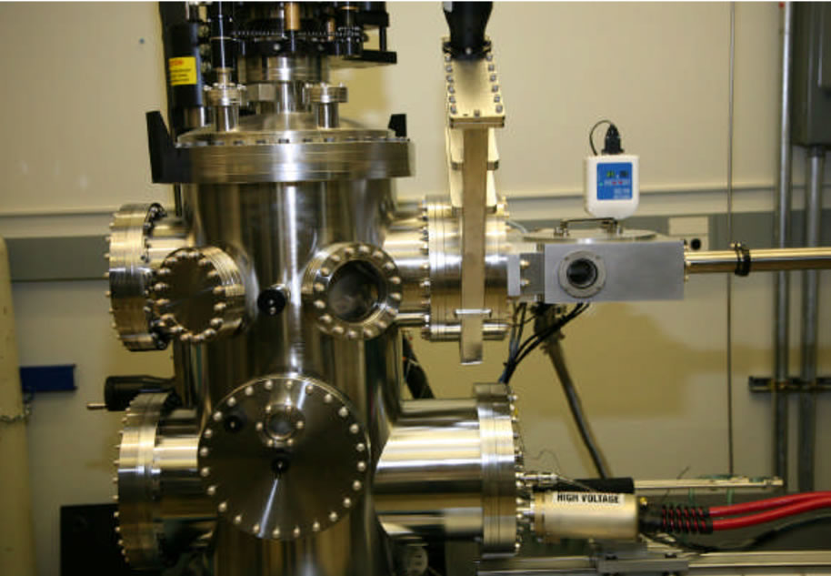
The a-SiGe samples studied in this work were deposited on oxide (SiO2/Si) Si wafers by e-beam evaporation method using an ATC Orion 8-E evaporation system. Figure 1 shows the picture and schematic of the evaporation system used for the sample preparation. The substrates were cleaned using acetone, methanol, isopropanol and de-ionized water. The substrate temperature was 200˚C. An e-beam power of 1.75 kW was used to evaporate the source material of mixed pellets of silicon and germanium with appropriate weight ratio. Film composition variations were obtained by changing the weight ratio of SiGe mixture. Post deposition hydrogenation were carried out for 30 minutes at 200˚C, 10 sccm H2 flow, 100 mTorr pressure, and 50 watts RF plasma power.
Rutherford back scattering (RBS) analysis was used to
 (a)
(a)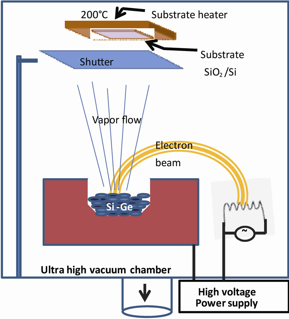 (b)
(b)
Figure 1. Silicon-Germanium thin film deposition system. (a) Image and (b) schematic of e-beam evaporation system that used to deposit thin film of Si1–xGex at various compositions (x) by evaporating mixed materials of silicon and germanium with appropriate weight ratios.
evaluate the film composition and uniformity. RBS analysis was done using a 1.5 MeV He+-ion beam, and two detectors positioned at scattering angles of 167˚ and 135˚, in the laboratory (IBM) geometry. The crystallographic structure of the film was analyzed by X-ray diffraction (XRD) and carried out using a Scintag X-ray diffractometer equipped with a Cu Kα X-ray source (λ = 1.54 Å) and a horizontal wide-angle four-axis goniometer with stepping motors which allowed independent or coupled theta/2- theta axes motion. XRD patterns were collected using a Theta/2-theta scan.
An Ellipsometer, Model TFProbe SE200BA, made by Angstrom Sun Technologies, Inc., was used to determine optical constants and absorption coefficient of the films. Raman spectroscopy of the films was carried out using a Renishaw inVia confocal Raman spectrometer equipped with a research-grade Leica microscope, 20 × objective (numerical aperture of 0.40), and WiRE 2.0 software. A 785 nm laser light was utilized for excitation. The laser power on the sample was about 115 mW.
A Woollham Dual Rotating Compensator with a quartz tungsten halogen and deuterium lamp was used to measure transmission curves from 245 nm to 1200 nm. From this data the absorption coefficients (α) were determined using the equation:
 (1)
(1)
where t is the film thickness, α the absorption coefficient, IT the intensity of transmitted light, and Io is the intensity of initial light. The optical bandgap is related to the absorption coefficient by:
 (2)
(2)
where K is a constant, Eg the optical bandgap, n is 1/2 for direct bandgap and hu is the photon energy. Using the calculated absorption coefficients, plots of (αhu)2 vs hu produced [10] . The x-axis intercept of a liner fit to each plot was used to estimate the optical bandgap of films. It is important to note that these calculations do not account for possible interference effects from reflection, which is assumed to be minimal due to the low film thicknesses.
3. Results and Discussion
All deposited films in this work were thoroughly characterized by RBS, XRD, Ellipsometer, Raman and optical spectroscopy. The as-deposited SiGe films have uniform composition as controlled by the source Si-Ge weight ratio. For illustration purposes, Figure 2 shows the results of RBS measurements for two different samples deposited using two different mixtures of Si-Ge source materials with weight ratio 2:1 and 16:1. The yield tails at approximately channel 600, 550, and 350 corresponds to Si in the SiGe film, SiO2 layer and Si wafer respectively, while the yield tails at approximately channel 850 corresponds to Ge in the SiGe film. The channel thickness and composition (x) are interdependent, and good fits can be obtained for Ge composition 85 at.% and 32 at.%. Assuming a pure Ge channel with the bulk density, the thickness the two different composition films are 60 and 66 nm respectively. The uniformity of the film is evidenced by the symmetry of the Ge peak.
All the films used in this study are amorphous. This is shown in Figure 3. It shows the X-ray diffraction patterns of Si1–xGex with x = 0.32 and 0.47. Except for a peak close to 2 theta angle of 70 degree, no crystalline phase has been observed, indicating amorphous structure of the films. The observed peak arises from the Si crystalline wafer. Similar results were observed for the entire set of films used in this study.
Raman spectroscopy observation also confirms the amorphous structure of these films. Figure 4 shows a series
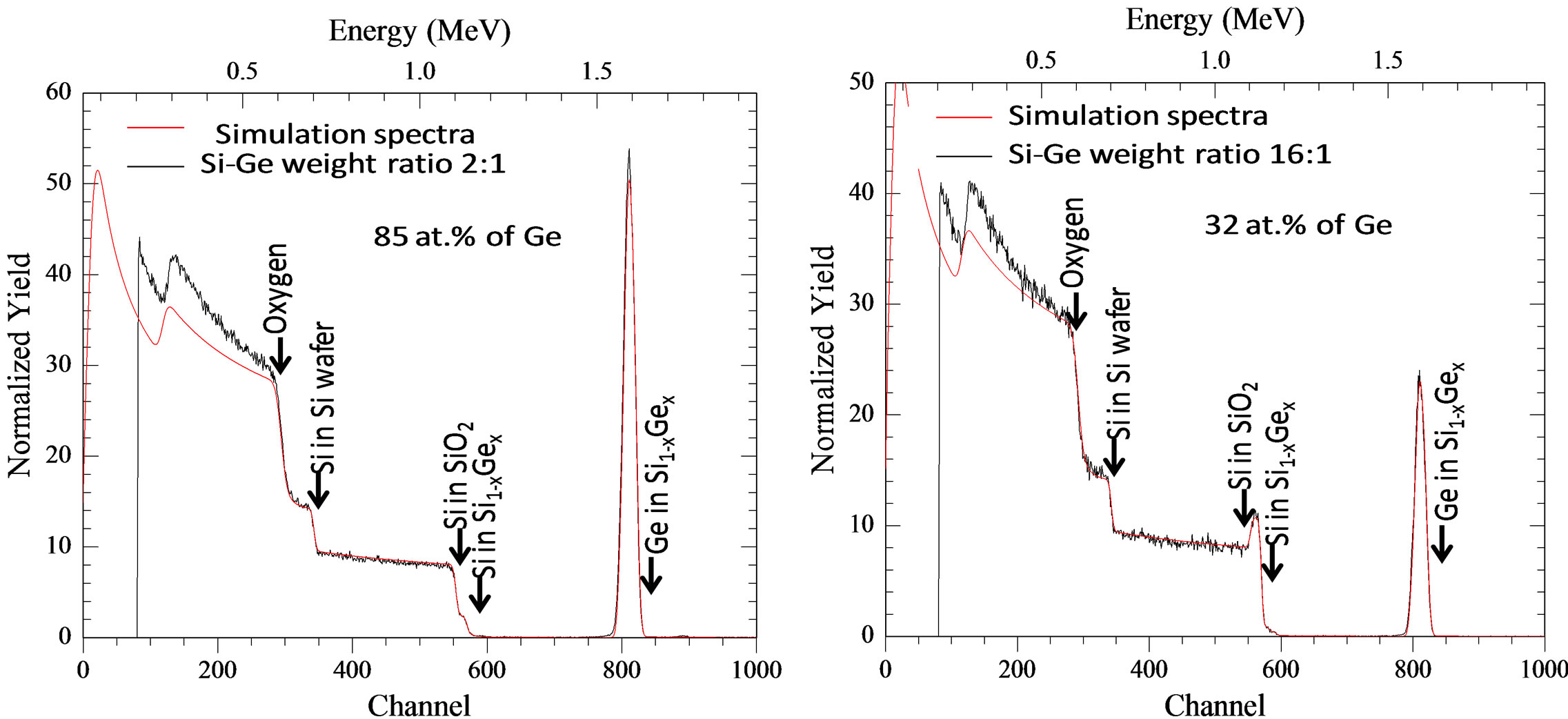
Figure 2. Compositional analysis. Rutherford backscattering spectra of Si1–xGex thin films produced by evaporating mixed material of silicon-germanium with weight ratios 2:1 (left) and 16:1 (right). The red line show the simulation spectra obtained for compositions 85 at.% (left) and 32 at.% (right) of Ge.
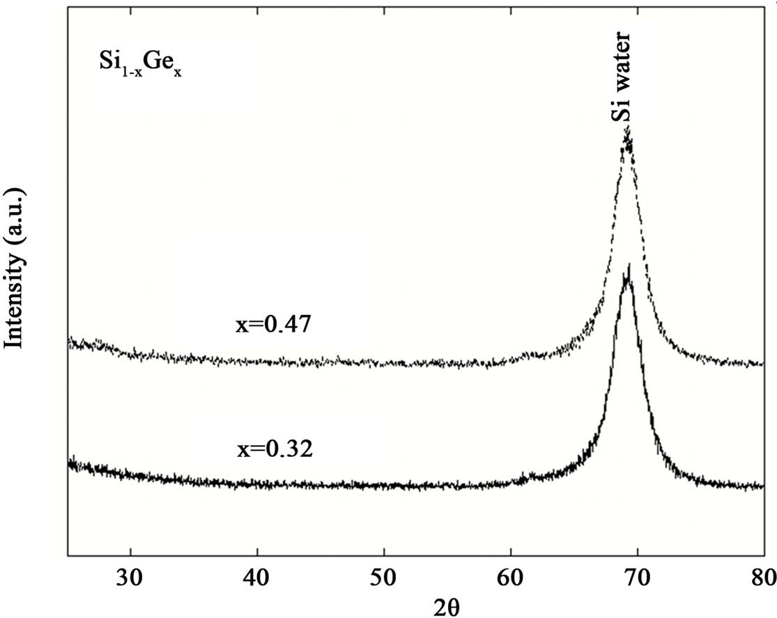
Figure 3. Structural property. X-ray diffraction patterns of Si1–xGex thin films with Ge fractions 0.32 (lower pattern) and 0.47 (upper pattern). The peak observed at 2θ theta vablue close to 70˚ attributed to the Si substrate. SiGe crystalline peaks are absent in these patterns.
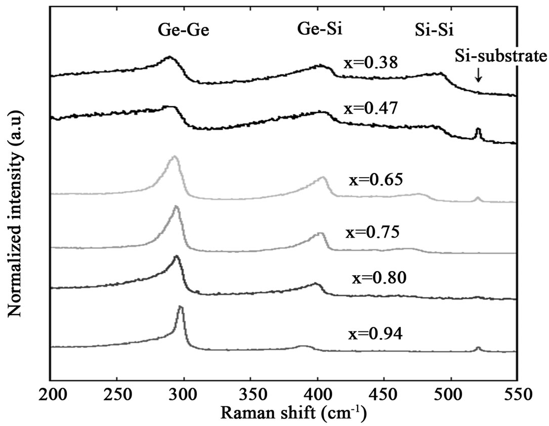
Figure 4. Raman spectroscopy scan of a-Si1–xGex films with Ge fraction range from 0.38 to 0.94 (top to bottom spectra). The peaks at 300, 400 and 480 cm–1 corresponds to Ge-Ge, Si-Ge and Si-Si modes. Substrate signal observed at 520 cm–1. Strain induced peak shift and crystallinity dependent peak broadening is observed.
of Raman spectra taken on Si1–xGex films with x ranging from 0.32 to 0.95. Besides the Si substrate signal at 520 cm–1, Ge-Ge, Si-Ge and Si-Si vibrational peaks can be seen at about 300, 400 and 480 cm–1 respectively [11].
Transverse optic Ge-Ge mode (~300 cm–1) is observed in all samples. As the Ge concentration increases, the GeGe optic mode peak intensity increases, accompanied with a reduced peak width, indicating improvement in film crystallinity, particularly in the film with x = 0.94. Azuma et al. [12] reported a preferential growth orientation for Si1–xGex crystal at x > 0.9. Observation of the Ge-Si band in all the films indicates the formation of SiGe in the film. As the Ge fraction increases, the intensity of SiGe peak intensity slightly decreases indicating a reduction in Si-Ge bonds, and the Ge-Ge optic mode peak shows red-shift towards higher wave-number while the Si-Ge peak shows a red-shift towards lower wave numbers. It is well known that strain in the SiGe films shift the peak without changing the full width half maxima of the peak [13]. The observed red-shift is due to the strain originated from the difference of the liner thermal expansion coefficient between SiGe layer with different composition of Ge (5.8 × 10⁻⁶ K–1), Si (2.6 × 10⁻⁶ K–1) and SiO2 (3.25 × 10⁻⁶ K–1) [11]. The variation in thermal expansion co-efficient leads to tensile stress in Ge rich film and compressive stress in Si rich films. Hence, the incorporation of Ge influences the film crystallinity and strain. The presence of strain influences the bandgap of the SiGe film [2].
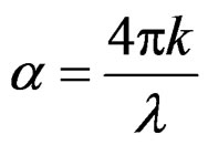
The optical absorption coefficient (α) of a-SiGe films with Ge fraction of 0.22, 0.48 and 0.94 was obtained from extinction coefficient (k) according to the relation:
 (3)
(3)
where λ is the wavelength of the light. The extinction coefficient is extracted from the spectroscopic ellipsometry measurements. Figure 5 shows the calculated absorption coefficient of the Si1–xGex film with x = 0.22, 0.48 and 0.94. Also it shows a comparison between the absorption coefficient of a-Si (solid circle) [14] and Si0.52Ge0.48 (open circle) at 700 nm. It clearly shows that Ge incurporation systematically increases the absorption coefficient of the film. Similar result has been observed by C. Wang et al. [15] on a-SiGe film, grown by very high frequency plasma enhanced chemical vapor deposition method. The absorption coefficient of a-SiGe is more than one order of magniture higher than a-Si film at 700 nm. As the Ge fraction increases, photosensitivity of a-SiGe film extends into IR band of solar spectrum.
The energy bandgap of the a-SiGe film decreases as the Ge fraction in a-SiGe film increases. This is shown in Figure 6. It shows the calculated optical bandgap as a function of Ge fraction. The bandgap various from 1.7 to 0.92 eV for Ge fraction from 0.22 to 0.94 at.%. The amorphous nature of the film provides a wider window of bandgap energy and direct bandgap characteristics. The presence of strain in the film also contributes to changes in the bandgap energy. Hence, bandgap and photo-sensitivity of a-SiGe films can be easily tuned by changing Si and Ge weight ratio of the evaporation source material mixture.
4. Summary
Amorphous SiGe films have been fabricated by e-beam evaporation in an ultra high vacuum chamber. The influence of the Ge fraction on the structural, optical and bandgap properties of the film was investigated. For the entire range of Ge fractions, the SiGe films are amorphous, although the film with Ge fraction about 0.9 shows some sign of improvement in Ge crystallinity. The Ge rich films are in tensile stress and the Si rich films are in compressive stress. As the Ge fraction in the a-SiGe film increases, the absorption coefficient increases and the bandgap decreases systematically and its photosensitivity extends into IR band of the solar spectrum. Our study proves that the a-SiGe films are a tunable absorber layer, suitable for wider spectrum optoelectronic device applications such as photo-detector and photovoltaic devices.
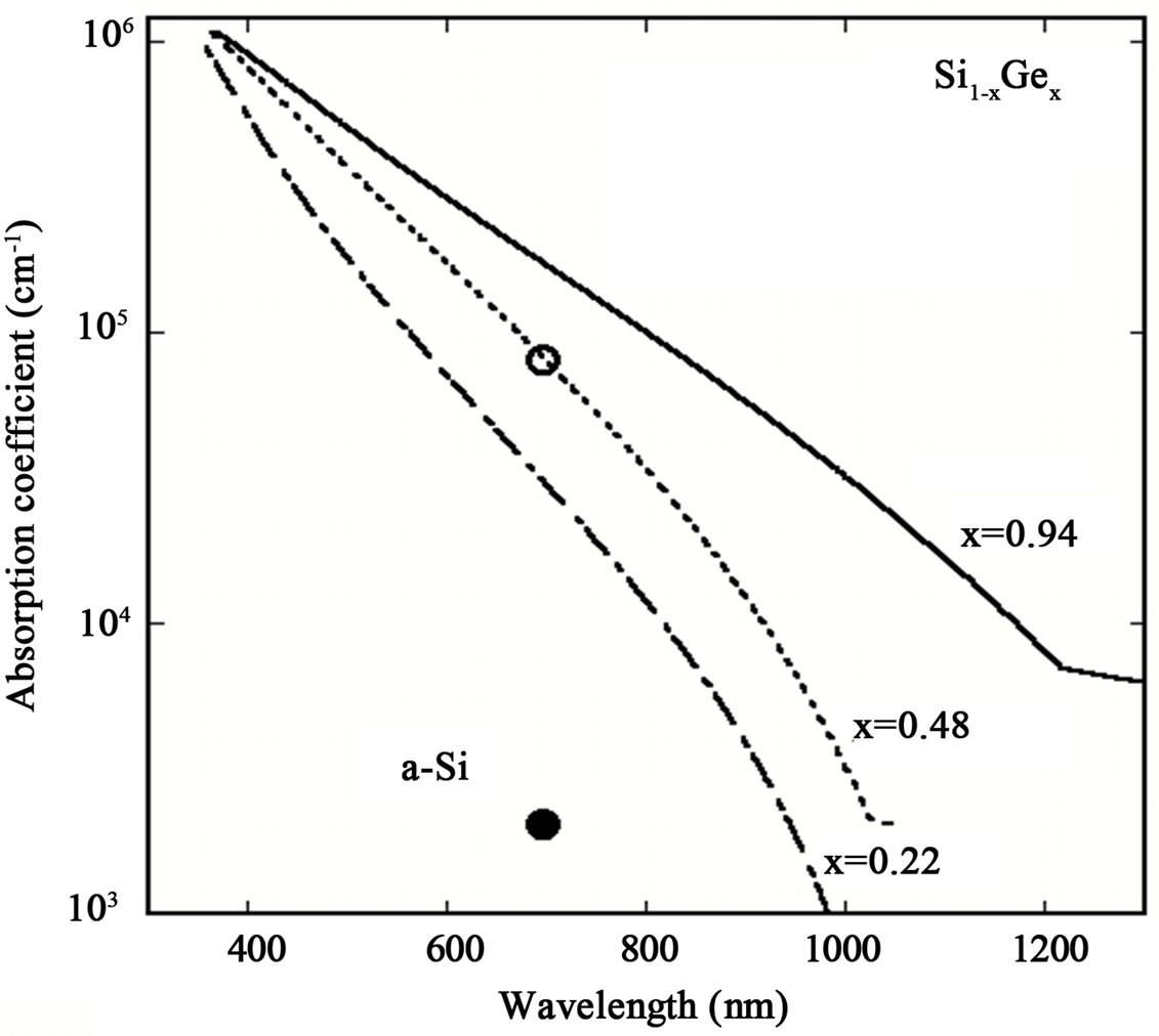
Figure 5. Absorption coefficient spectra of a-Si1–xGex thin films with x = 0.22, 0.48 and 0.94. Absorption coefficient of a-Si (solid circle) [14] is compared with a-Si0.52Ge0.48 (open circle) at wavelength 700 nm. Ge incorporation increases the absorption coefficient and extends its photosensitivity towards longer wavelengths.
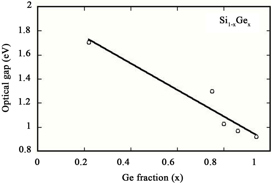
Figure 6. Bandgap tuning. Optical bandgap of a-Si1–xGex thin film as a function of Ge fraction (x). As the Ge fraction increases, the bandgap of SiGe film decreases.
5. Acknowledgements
The authors would like to thank NYSERDA for supporting the SiGe development program for solar cell applications.
REFERENCES
- D. V. Lang, R. People, J. C. Bean and A. M. Sergent, “Measurement of the Band Gap of GexSi1–x/Si StrainedLayer Heterostructures,” Applied Physics Letters, Vol. 47, No. 12, 1985, pp. 1333-1335. doi:10.1063/1.96271
- N. Usami, T. Ichitsubo, T. Ujihara, T. Takahashi, K. Fujiwara, G. Sazaki and K. Nakajima, “Influence of the Elastic Strain on the Band Structure of Ellipsoidal SiGe Coherenty Embedded in the Si Matrix,” Journal of Applied Physics, Vol. 94, No. 2, 2003, pp. 916-920. doi:10.1063/1.1580194
- R. Braunstein, A. R. Moore and F. Herman, “Intrinsic Optical Absorption in Germanium-Silicon Alloys,” Physical Review, Vol. 109, No. 3, 1958, pp. 695-710. doi:10.1103/PhysRev.109.695
- K. H. Jun, J. K. Rath and R. E. I. Schropp, “Enhanced Light-Absorption and Photo-Sensitivity in Amorphous Silicon Germanium/Amorphous Silicon Multilayer,” Solar Energy Materials & Solar Cells, Vol. 74, No. 1-4, 2002, pp. 357-363. doi:10.1016/S0927-0248(02)00095-8
- K. Nakajima, K. Fujiwara, W. Pan, N. Usami and T. Shishido, “Growth and Properties of SiGe Multicrystals with Microscopic Compositional Distribution and Their Applications for High-Efficiency Solar Cells,” Journal of Crystal Growth, Vol. 275, No. 1-2, 2005, pp. e455-e460. doi:10.1016/j.jcrysgro.2004.11.019
- E. Maruyama, S. Okamoto, A. Terakawa, W. Shinohara, M. Tanaka and S. Kiyama, “Towards Stabilized 10% Efficiency of Large-Area (>5000 cm2) a-Si/a-SiGe Tandem Solar Cells Using High-Rate Deposition,” Solar Energy Materials & Solar Cells, Vol. 71, No. 1-4, 2002, pp. 339- 349. doi:10.1016/S0927-0248(02)00093-4
- P. Wickboldt, D. Pang, W. Paul, J. H. Chen, F. Zhong, C.-C. Chen, J. D. Cohen and D. L. Williamson, “High Performance Glow Discharge a-Si1–xGex:H of Large x,” Journal of Applied Physics, Vol. 81, No. 9, 1997, pp. 6252-6267. doi:10.1063/1.364413
- M. Serenyi, J. Betko, A. Nemcsics, N. Q. Khanh, D. K. Basa and M. Morvic, “Study on the RF Sputtered Hydrogenated Amorphous Silicon-Germanium Thin Films,” Microelectronics Reliability, Vol. 45, No. 7-8, 2005, pp. 1252-1256. doi:10.1016/j.microrel.2005.02.008
- C. Eisele, M. Berger, M. Nerding, H. P. Strunk, C. E. Nebel and M. Stutzmann, “Laser-Crystallized Microcrystalline SiGe Alloy for Thin Film Solar Cells,” Thin Sold Films, Vol. 427, No. 1-2, 2003, pp. 176-180. doi:10.1016/S0040-6090(02)01216-6
- D. Dwyer, R. Sun, H. Efstathiadis and P. Haldar, “Characterization of Chemical Bath Deposited Buffer Layers for Thin Film Solar Cell Applications,” Physica Status Solidi (A), Vol. 207, No. 10, 2010, pp. 2272-2278. doi:10.1002/pssa.201025522
- C.-Y. Tsao, Z. Liu, X. Hao and M. A. Green, “In Situ Growth of Ge-Rich Poly-SiGe:H Thin Films on Glass by RF Magnetron Sputtering for Photovoltaic Applications,” Applied Surface Science, Vol. 257, No. 9, 2011, pp. 4354- 4359. doi:10.1016/j.apsusc.2010.12.058
- Y. Azuma, N. Usami, K. Fujiwara, T. Ujihara and K. Nakajima, “A Simple Approach to Determine Preferential Growth Orientation Using Multiple Seed Crystals with Random Orientations and Its Utilization for Seed Optimization to Restrain Polycrystallization of SiGe Bulk Crystal,” Journal of Crystal Growth, Vol. 276, No. 3-4, 2005, pp. 393-400. doi:10.1016/j.jcrysgro.2004.11.430
- W. K. Choi, L. K. The, L. K. Bera and W. K. Chim, “Microstructural Characterization of rf Sputtered Polycrystalline Silicon Germanium Films,” Journal of Applied Physics, Vol. 91, No. 1, 2002, pp. 444-449. doi:10.1063/1.1423388
- M. K. Bhan, L. K. Malhotra and C. Kashyap, “Electrical and Optical Properties of Hydrogenated Amorphous Silicon Germnanium (a-Si1–xGex:H) Films Prepared by Reactive Ion Beam Sputtering,” Journal of Applied Physics, Vol. 66, No. 6, 1989, pp. 2528-2537. doi:10.1063/1.344243
- C.-C. Wang, C.-Y. Liu, S.-Y. Lien, K.-W. Weng, J.-J. Huang, C.-F. Chen and D.-S. Wu, “Hydrogenated Amorphous Silicon-Germanium Thin Films with a Narrow Band Gap for Silicon-Based Solar Cells,” Applied Physics, Vol. 11, No. 1, 2011, pp. S50-S53.