Circuits and Systems
Vol.09 No.11(2018), Article ID:88777,17 pages
10.4236/cs.2018.911018
Simulation of Space Charge Impact on Partial Discharge Inception Voltage in Power Busbars Dedicated to Future Hybrid Aircrafts
Mallys Elliazar Banda*, David Malec, Jean-Pascal Cambronne
Laboratoire de Plasma et Conversion d’Energie, Université de Toulouse-CNRS-INPT-UPS, France

Copyright © 2018 by author(s) and Scientific Research Publishing Inc.
This work is licensed under the Creative Commons Attribution International License (CC BY 4.0).
http://creativecommons.org/licenses/by/4.0/


Received: September 5, 2018; Accepted: November 24, 2018; Published: November 27, 2018
ABSTRACT
Reducing greenhouse gases, saving energy resources and mass optimization require technological changes towards increasingly electric vehicles. At the same time, performance improvement of semiconductor and dielectric materials further promotes electronic components confinement, resulting in a significant increase of embedded power densities. In the particular case of future hybrid propulsion aircrafts, electrical power that intended to supply reactors would be converted through power electronics components mounted on power busbars and insulated by solid dielectrics materials. These dielectrics materials have to respond to various electrical constraints of use (HVDC), in spite of environment change of aircraft parameters such as low pressure, temperature and thermal cycles, humidity... Unfortunately, partial discharges phenomenon is the most problem within electrical insulation system (EIS). Based on a topological model of power busbars designed for power converters dedicated to hybrid aircraft, partial discharge studies were conducted by simulation in various charging conditions of a PTFE insulator. Simulation results, which focus on electric field thresholds criteria of partial discharge inception voltage in air, reveal a net sensitivity of a space charge accumulation and distribution on dielectrics behaviour even for low space charge density, depending on their location in dielectrics. Compared to the behaviour observed with implanted homocharges, when by increasing homocharges density from 0.5 C/m3 to 2 C/m3 we observe a decrease of electric field by 450%, simulation results show a highest risk of partial discharge inception when heterocharges are accumulated inside dielectrics. Their accumulation increases the electric field in triple points beyond electric field thresholds of partial discharge inception in air. The simulated electric field reaching 22 kV/mm with only 2 C/m3 of heterocharges density accumulated in dielectric/busbars interfaces.
Keywords:
Simulation, Partial Discharge, Space Charge, Power Busbars, Hybrid Aircraft

1. Introduction
Increase environmental impact of greenhouse gas emissions induced by air transport requires substituting pollutant fuel propulsion by cleanest propulsion systems. Hybrid propulsion systems expected for short-term time and entirely electric propulsion systems expected for long-term time represent a new technological challenge [1] [2] . This challenge includes power conversion and distribution systems which are able to supply the future hybrid/electric propulsion devices. These power converters are generally supplied through laminated busbars which are insulated by solid organic dielectrics, most of time made of polymers materials. Among available insulators, PTFE films are often used [3] .
However, in many case, triple material regions appear in such powered systems, with many “conductor-air-insulator” junction points. These triple points play an important role in electric field enhancement [4] - [10] . In the case of electric field induced by electric charges, it well established that charges behaviour impacts the flashover inception in solid dielectrics materials [4] . Their polarity, magnitude as well as the shape of their distribution could have a considerable effect on the field enhancement at insulator-vacuum interfaces [5] . Until now, previous works had brought out the electric field enhanced near either the cathode or the anode, depending on whether the angle of the interface and the both case of charged and uncharged interfaces. Mainly for surface charging cases induced by secondary electron avalanche [4] [6] . If these important studies had already highlighted many aspects of electric field enhancement at triple points, its impact in regard of partial discharge risks at triple junction points remains a big question for electronics power designers since this region constitutes the weak point of insulation system, due to the mismatch between solid and gas permittivities [7] . For this reason, beside experimental measurements, more and more theoretical studies are performed to propose various analytical solutions of electric field distribution at triple point under conduction [8] [9] or geometrical effects [10] in triple point.
In power busbars application case, the triple point is constituted of busbars-insulator-air junction point. De facto, the both confinement and power densities increasing expose electric insulation systems to more partial discharge risks. Added to materials defects (structural and chemical defects, electronic traps distributions, trapping level…), these partial discharge inceptions locally increase the electric field within the dielectric material. This local increase in electric field changes the intrinsic material properties and reliability, with the consequence of an irreversible insulators damage of dielectric that can affect the insulation system and then expose the power converters on which the propulsion depends on [11] . Simulation proposed in this study aims to prevent the partial discharges risks in such systems. From charge accumulation hypotheses within power busbars insulating, this work is a contribution for a better understanding of induced charge mechanisms under electric field enhancement at triple point.
Based on a busbar topology from a power electronic converters, electric field cartographies were simulated around the most exposed triple points to partial discharge risks. Sandwiched between two copper busbars, a non-charged PTFE insulator is firstly subjected to a DC electric field of 2.5 kV/mm. In this case, two geometrical configurations are studied to highlight partial discharge risks to which the dielectric would be exposed. Secondly, hypothesis of a non-charged insulator is then replaced by an inhomogeneous accumulation of space charges through dielectrics: firstly, by homocharges and then by heterocharges. The impact of charge maximum density on implanted charges within dielectric as well as their spatial distribution on partial discharge risks at triple points are exposed and discussed.
2. Simulation Methodology
2.1. Converter Topology
Figure 1 shows a view of the studied power converter topology on which this study is based. It consists in seven busbars slats (2 mm-thick) mounted between input bus capacitors and fly output capacitors. Electronic component ships are packaged inside power modules embedded in below. The DC bus is powered by a DC 2.5 kV input voltage. PTFE films are sandwiched between each busbars pairs. In such topology, many triple points (air, solid dielectric, conductor) appear in busbars/PTFE/air interfaces. One of them, equivalent to the triple point with greatest potential difference, is zoomed in Figure 1 (at the right). Since this point is the one submitted to highest electric stress, it is also the most exposed to partial discharge risk, as well for transient as steady state, especially during strong electrical stress during flight phases (take-off and landing). For this reason,
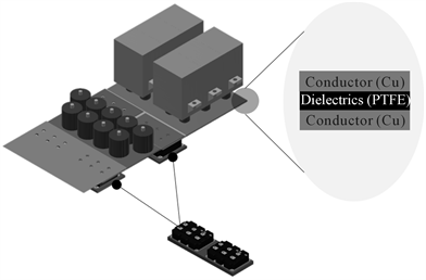
Figure 1. Schematic view of power busbars embedded inside a power electronics converter.
this study focuses on the estimation of partial discharges risks through electric field assessment in this triple point to characterize the insulation behaviour of busbars for this applied electric specification. Based on simulation results highlighted around this triple point, partial discharge risks incurred on this one would also reveal those expected on other triple points, since other triple points support lower electric potential differences.
2.2. Model Formulation and Simulation Conditions
A common way to evaluate if partial discharges occur between two conductor materials consists in comparison of Paschen theoretical and experimental curves obtained in considered gas where Paschen’s assumptions are applicable (uniformity of the electric field, plan/plan geometry of conductors, preponderance of electronic avalanche mechanism...) [12] . For air gaps greater than 1 mm (linear part of the Paschen curve), another alternative way would consist to assess the electric field distribution in a considered medium and to estimate the partial discharges risks by taking into account the breakdown threshold in air. This last way is the one used in this study. In accordance with the description of Figure 1, we consider two parallel copper busbars separated by a 1 mm-thick PTFE insulator (atmospheric pressure and room temperature), air is the surrounding medium. Figure 2 shows a schematization of the considered calculation domain.
The electric field is computed through finite elements method by solving Poisson’s equation in both air and dielectrics domains:
(1)
where is related to electric potential such as:
(2)
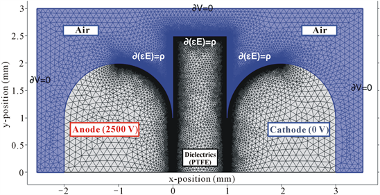
Figure 2. Calculation domain meshed (zoomed ´6) according to finite elements method. Neumann’s limit conditions were applied at air domain boundairies and Dirichlet’s limit conditions at electrodes. The remaining domain was submitted to poisson equation to solve electric field in all application domain. Meshing rafinement was reinforced at each domain boundary, with regular distribution. Stationnary calculation conditions.
is the space charge density, and the vacuum and relative permittivity, respectively. A zero flux was applied in air boundaries according to relation:
(3)
where is surface unit vector. The calculation domain was non-uniformly meshed. To increase calculation precision of electric field and charge at the interfaces, refinement was added to both boundaries and in triple points as shown in Figure 2. The total meshing was sized in 7.5 * 105 finite elements.
2.3. Numerical Implementation
The model was implemented in finite element numerical method through Comsol Multiphysics® 5.2a software (CM). The simulation was based on Partial Differential Equation (PDE) sub-module embedded in the mathematics module. Firstly, the 2D-geometry was built to reproduce calculation domain shown in Figure 2, followed by filling of all computational parameters. The Poisson-Equation module (poeq) was added to solve model equation from Equations (1) to (3). Neumann limit conditions were settled in air external boundaries, and Dirichlet limit conditions were inserted on busbars electrodes (i.e., grounded condition at cathode and +2.5 kV voltage condition at anode). The model is computed in stationary conditions. The calculation begins by the initialization of all simulation parameters. Then, all limit conditions were applied (electric potential, zero fluxes and net charge density) and knowing charge density, internal BDF solvers [13] compute the electric field in air and dielectrics by solving Poisson Equation (1). Results are then post-treated to plot space charge, electric potential and field cartographies.
3. Results and Discussion
3.1. Geometry Impact on Partial Discharge
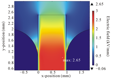
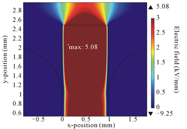
In a first step, the conventional configuration keeping dielectric and busbars in same lengths was compared with a curved busbars configuration (curving radius ~1 mm). Figure 3 shows cartographies of electric potential and electric field for both geometrical configurations.
The electrical potential cartographies show apparent similarities with both simulated configurations. The geometric change on busbars (see Figure 3(c)) do not seem to affect the electrical potential distribution in large extend (see Figure 3(a)). This observation is less the case for electric field cartographies. Electric field is highest in classic configuration compared to curving one. The maximum electric field decreases from 9.15 kV/mm (see Figure 3(b)) to 6.5 kV/mm (see Figure 3(d)) by curving busbars. For both configurations, an electric field enhancement is observed at two triple points (Air-Cu-PTFE regions). We also observe a better uniformity of the electric field within the dielectric in a classic busbar geometry.
 (a)
(a)
 (b)
(b)
 (c)
(c)
 (d)
(d)
Figure 3. Cartographies of electric potentials ((a), (c)) and electric fields ((b), (d)) simulated according to conditions described at Figure 2. ((a), (b)) classic busbars configuration, ((c), (d)) curving busbars configuration. Non-charged dielectrics (PTFE).
From a partial discharges point of view, for a DC 2.5 kV/mm applied voltage, both configurations lead to a much higher electric field than the breakdown field admitted in air at atmospheric pressure and at ambient temperature ( 3 kV/mm) [11] [12] . Implying that air is, among the three materials, the most exposed to partial discharge risks, because of its low permittivity, ionization processes more accentuated in air and avalanche mechanisms speed occurring inside which facilitate others electronic processes. The risks of partial discharge inception would seem inevitable in both geometrical configurations at triple points, at least because of favourable electric fields in air. Triple points would be the most sensitive region to these partial discharge risks and these would be more accentuated with classical configuration than the curved one. Next results will be therefore presented only based on curving configuration of busbars.
Taking into account the advantages (electric field decrease at triple points) obtained with curved geometrical configuration, another simulation was performed to more decrease electric field in air, and thus limit partial discharge risks at triple points, by ranging dielectric length relative to conductor length. Figures 4(a)-(d) show the electric field cartographies obtained for four distinct dielectric heights: 2.5 mm (Figure 4(a)), 2 mm (Figure 4(b)), 1.5 mm (Figure 4(c)) and 1 mm (Figure 4(d)).
Reducing length of dielectrics sandwiched between busbars is accompanied by a drastic reduction of the electric field in the air, and more sensitively within the triple points. By changing from a dielectric length of 2.5 mm (see Figure 4(a)) to 1 mm (see Figure 4(d)), the electric field is divided by 2.35. This decrease is greater for a dielectric length of 1 mm.
This electric field reduction also decreases the electric field confinement within triple points, thereby decrease potential gradient at these locations. Thus, by decreasing confinement regions, it is also possible to reduce electric field reinforcement in air. However, although this dielectric length reduction decreases, electric field between busbars, it represents a high partial discharge risk due to resulting electric field amplitude near of air breakdown threshold (2.76 kV/mm - 3kV/mm), since both conductors (busbars) will be separated only by air gap. This geometric configuration is therefore not better to prevent partial discharges around busbars. The elongation from Figure 4(a) will certainly remain the best
 (a)
(a)
 (b)
(b)
 (c)
(c)
 (d)
(d)
Figure 4. Cartographies of simulated electric fields for four dielectrics length: 2.5 mm (a), 2 mm (b), 1.5 mm (c) and 1 mm (d). Simulation conditions from Figure 2. Non-charged dielectrics (PTFE).
geometrical configuration, since the two conductors are separated by a solid insulator having a larger breakdown voltage threshold than air.
3.2. Space Charges Impact on Partial Discharge
3.2.1. Homocharges Impact
Now the assumption of a perfectly non-charged dielectric is replaced by a more realistic charged one, considering an initial charge state due to homocharges deposition (charges of same sign than electrode polarities) at busbars/dielectrics interfaces then polarized by a DC 2.5 kV/mm electric field. Figure 5 shows the simulated distribution of space charge. In first (Figure 5(a)), the homocharges were implanted at 50 μm from each surface of insulator and their amplitude is then ranged from 0 C/m3 to 2 C/m3. In second (Figure 5(b)), the implanted charge level was maintained at 0.01 C/m3 while their distribution was ranging in insulator bulk. These charge hypotheses are consistent with the experimental observations and aging studies for PTFE dielectrics dedicated to power electronics busbars isolation [14] [15] .
・ Simulated electric field due to gradual homocharges densities: Figure 6 shows the cartographies of simulated electric field obtained in the case of homocharges implantation near to dielectrics surface with charge densities ranging from 0 C/m3 to 2 C/m3. The maximum of calculated electric field in air and dielectrics material (PTFE), induced by homocharges, are presented in Table 1.
 (a)
(a)  (b)
(b)
Figure 5. Simulated homocharges implantation inside dielectrics material sandwiched between two busbars conductors (conditions described in Figure 2(a)) Homocharges implantation at 50 µm from surface, (b) homocharges trransportation through dielectrics volume for a fixed charge amplitude.

Table 1. Maximum of electric field in air and PTFE with homocharge.
 (a)
(a)
 (b)
(b)
 (c)
(c)
 (d)
(d)
 (e)
(e)
 (f)
(f)
Figure 6. Simulated electric field associated to homocharges shown in Figure 5(a). Absolute charge density of (a) 0 C/m3, (b) 0.01 C/m3, (c) 0.1 C/m3, (d) 0.5 C/m3, (e) 1 C/m3 and (f) 2 C/m3.
For densities of charges lower than 0.1 C/m3 (Figures 6(a)-(c)), simulated electric field is maximum in air and higher than the breakdown threshold (>3 kV/mm). Beyond that, for charge densities exceeding 0.5 C/m3 (Figures 5(d)-(f)), maximum of electric field is located within the dielectrics bulk. The maximum of electric field decreases by 450% when amplitude of charge density increases from 0.5 C/m3 (Figure 5(d)) to 2 C/m3 (Figure 5(f)). In summary, the higher the homocharges density the lower the electric field at the interface busbars/dielectrics and the higher the electric field within the PTFE. This charge behavior is in good agreement with usually reported experimental studies [7] [16] .
More homocharges accumulation near dielectric surface seems to decrease electric field at the triple points (for densities greater than 1 C/m3). Although such considered charge densities of homocharges accumulated in dielectrics bulk could prevent partial discharge risks in air, it could however generate a gradual accumulation of homocharges that would increase the electric field to upper dielectric/air interface. This increase could create premature electron/hole pairs and generate others ionization processes in favour of partial discharges.
・ Simulated electric field due to gradual homocharges distribution: Now the charge density was fixed to 0.01 C/m3. In this case, only spatial distribution of homocharges through the dielectrics bulk is ranged from 1 to 300 μm. Figure 7 shows the simulated electric field cartographies associated to charge densities illustrated in Figure 5(b).
Even with weaker distribution of homocharges, the electric field remains important within triple points whereas it is weak in the dielectrics bulk. When charge
 (a)
(a)
 (b)
(b)
 (c)
(c)
 (d)
(d)
Figure 7. Simulated electric field associated to homocharges shown in Figure 5(b). Fixed charge density of 0.01 C/m3 for four charge distribution (a) 1 µm, (b) 50 µm, (c) 100 µm and (d) 300 µm.
distribution through dielectric bulk increase from 1 μm to 300 μm, the maximum of electric field is almost halved. This decrease is observed especially at triple points while the electric field continues to grow in volume. The transport of homocharges from both dielectrics interfaces creates a recombination zone of heterocharges in dielectrics bulk, that increase electric field in insulator material. As observed with previous results under variation of homocharges densities presented in Figure 6, ranging of homocharges distribution also affects electric field as well at interfaces and within dielectrics bulk.
As well for static implantation near busbars/insulator interfaces as for spatial ranging of their distribution inside insulator, accumulation of homocharges within insulating material sandwiched between busbars would qualitatively and quantitatively affects distribution electric field in the dielectric. It would seem that for a charge density below 0.5 C/m3, the electric field due to homocharges would not be sufficient to impact the total electric field in material and consequently at the triple points, although this threshold would not be the unique conditions to generate a partial discharge in air since other physical and electronic processes should also be met [17] . However, it appears that partial discharge risks would be attenuated with higher homocharges accumulation (above 0.5 C/m3) at insulators/busbars interfaces.
From charge generation and transport mechanisms point of view, polarization of a polymeric solid insulators such as PTFE under a DC electric field between copper conductive busbars would favour a preponderance of homocharges injection on other generation mechanisms. This would seem theoretically favourable to reduce partial discharge risks if heterocharges zones are not generate at the interfaces of busbar/insulator. Increasing strong homocharges injection at busbar/insulator interfaces would thus be possible to decrease interfacial electric field, and consequently reduce electric field in triple points of circuits and systems, which are moreover areas most exposed to partial discharges risks under these topological conditions.
3.2.2. Heterocharges Impact
Based on a reverse reasoning, homocharges is now replaced by heterocharges implantation (charges of opposite sign to the electrode polarities). First, the heterocharges are implanted at the same place within the dielectric material, for six different densities (see Figure 8(a)). Then, charge density was fixed to 0.01 C/m3 and these heterocharges are spatially distributed within dielectrics bulk (Figure 8(b)). The simulations of the two heterocharges implantations type are shown in Figure 8.
・ Simulated electric field due to gradual heterocharges densities: The simulated electric field cartographies corresponding to heterocharges implantation with charge densities ranging (Figure 8(a)) are exposed in Figure 9. In presence of heterocharges close to the dielectric surface, the electric field rapidly grows in triple points and at dielectric surface. This increasing depends on charge density, while it decreases considerably in the volume of the insulator. This behaviour is the contrary of what observed with homocharges (Figure 6). The maximum of calculated electric field in air and dielectrics material (PTFE), induced by heterocharges, are presented in Table 2.
 (a)
(a)  (b)
(b)
Figure 8. Simulated heterocharges implantation inside dielectrics sandwiched between two busbars in conditions described in Figure 2. Symetrical situation compared to Figure 5. (a) Heteroharges implantation at 50 µm from dielectrics surface; (b) Heterocharges transportation through dielectrics bulk for a fixed charge density.
 (a)
(a)
 (b)
(b)
 (c)
(c)
 (d)
(d)
 (e)
(e)
 (f)
(f)
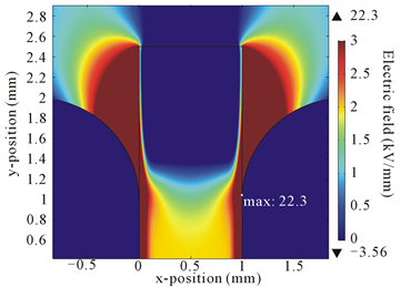
Figure 9. Simulated electric field associated to heterocharges shown in Figure 8(a). Absolute charge density of (a) 0 C/m3, (b) 0.01 C/m3, (c) 0.1 C/m3, (d) 0.5 C/m3, (e) 1 C/m3 and (f) 2 C/m3.
Table 2. Maximum of electric field in air and PTFE with heterocharge.
Electric field massively increase in air despite small implanted heterocharge densities. Resulting electric field in air is seven times higher than breakdown threshold necessary to initiate partial discharge [11] . Simulated electric field reaches up to 22 kV/mm for only 2 C/m3 of heterocharges density. A peak of electric field is always located in air at the triple points. Likewise, the electric field is more concentrated at the busbar/insulator interfaces, reinforcing the increase of electric field within and around the triple points. The distribution of electric field in dielectric bulk is also inhomogeneous, it seems to be distributed over two opposite zones along the horizontal axis of the dielectrics, with an electric field five times more intense in top air/insulator interface than above.
・ Simulated electric field due to gradual heterocharges distribution: In the last simulation, the heterocharges distribution within dielectric was changed according to Figure 8(b). Simulated results of electric fields for these conditions are shown in Figure 10.
When heterocharges are extended over 1 μm from busbar/insulator interfaces (Figure 10(a)), the resulting electric field at triple points is twice more than air discharge threshold. By extending distribution of the heterocharges over 50 μm (Figure 10(b)), 100 μm (Figure 10(c)) and 300 μm (Figure 10(d)), electric field induced by heterocharges increases continuously and remains greater than discharges threshold in triple points. It reaches more than triple of air discharge threshold for a heterocharge distribution over 300 μm (~9 kV/mm). So, the more the distribution of heterocharges, the higher the electric field at busbar/insulator interfaces and the lower the electric field in volume. This behaviour has already been reported [7] [9] .
 (a)
(a)
 (b)
(b)
 (c)
(c)
 (d)
(d)
Figure 10. Simulated electric field associated to heterocharges shown in Figure 8(b). Fixed charge density of 0.01 C/m3 for four charge distribution (a) 1 µm, (b) 50 µm, (c) 100 µm and (d) 300 µm.
Various mechanisms could cause heterocharges accumulation in such solid insulating material polarized between busbars in a DC electric field. These heterocharges could be generated through natural traps within insulator, trapping distribution in dielectrics bulk, electrode/dielectrics interface defaults but also directly by extraction of charges towards busbars conductors due to a favourable internal electric field, chemical defaults or by detrapping processes induced by thermal activation through potential barrier. All these physical mechanisms that would make possible heterocharges accumulation would therefore be favourable to partial discharges inception in busbars environment [18] [19] . For this reason, although polarization in busbars configuration presented in this power circuit topology would not permit direct injection of heterocharges, prediction of their accumulation at busbar/insulator interface would require to carefully rethink industrial chain of insulators design dedicated to power converters intended to hybrid aircraft, in order to prevent partial discharge risks as highlighted by this study.
4. Conclusions
These simulations are a contribution to the study of partial discharge appearance, through analyse of space charges impact in a solid dielectric (PTFE) used for insulation of power busbars dedicated to hybrid aeronautical systems. Not only this study confirms that presence of space charges within a solid insulator generates an internal increase of electric field that impacts total electric field distribution, but it also highlights that for an applied electric field of 2.5 kV/mm, accumulation of small charges density in dielectrics (~0.01 C/m3), induced by example by some chemical defaults, thermal, pressure or mechanical stress, would be sufficient to anticipate partial discharges in air recovering busbars. Moreover, according to the sign of these charges, the risks of discharges would be differently appreciable. In case of homocharges accumulation at the busbars/insulator interfaces, electric field would tend to strengthen in dielectrics. This is less advantageously the case when these homocharges are transported in the volume of the dielectrics. On the contrary, heterocharges accumulation at busbar/insulator interfaces would reinforce the total electric field at insulator surface, leading to the greater risks of partial discharges resulting to the confinement of electric field at triple points. This situation would be accentuated as well by surface heterocharges density as their transport within the insulator bulk. Although PTFE is considered among the lower charging insulators, this study, applicable to other polymer insulators, reveals above all that charge accumulation of a few C/m3 would generate various mechanisms sufficient to age or activate degradation of insulators [18] [19] . In the intended case of hybrid-propulsion aircraft, electrical insulation system will be more exposed to partial discharge risks if insulation systems operate in thermal, humidity and pressure environmental conditions. In such condition, heterocharges accumulation would offer favourable conditions for partial discharges inception whose material, human and financial consequences could be irreversible. It is necessary to design non-charged insulation system in accordance to electrical strength intended for busbars to avoid any discharge inception. An alternative solution could be to screen busbars to ensure non-penetration of electric field in air gap, although this solution would increase weight density [20] .
Complementary experimental study is simultaneously underway to better understand the charge generation and transport mechanisms which could better help to predict partial discharge inception in organic solid dielectrics used for the isolation power converters busbars dedicated to hybrid propulsion. Results of this study will be the topic of other forthcoming investigations.
Acknowledgements
This project has received funding from the Clean Sky 2 Joint Undertaking under the European Union’s Horizon 2020 research and innovation program under grant agreement No. 715483.
Conflicts of Interest
The authors declare no conflicts of interest regarding the publication of this paper.
Cite this paper
Banda, M.E., Malec, D. and Cambronne, J.-P. (2018) Simulation of Space Charge Impact on Partial Discharge Inception Voltage in Power Busbars Dedicated to Future Hybrid Aircrafts. Circuits and Systems, 9, 196-212. https://doi.org/10.4236/cs.2018.911018
References
- 1. Kuhn, H., Seitz, A., Lorenz, L., Isikveren, A.T. and Sizmann, A. (2012) Progress and Perspectives of Electric Air Transport. Proceedings of the 28th International Congress of ICAS, Brisbane, Australia, 23-28 September 2012, 6.
- 2. Cotton, I., Nelms, A. and Husband, M. (2008) Higher Voltage Aircraft Power Systems. IEEE Aerospace and Electronic Systems Magazine, 23, 25-32. https://doi.org/10.1109/MAES.2008.4460728
- 3. Khachen, W., Suthar, J., Stokes, A., Dollinger, R. and Dunbar, W.G. (1993) Aerospace-Specific Design Guidelines for Electrical Insulation. IEEE Transactions on Electrical Insulation, 28, 876-886. https://doi.org/10.1109/14.237748
- 4. Bergeron, K.D. (1977) Theory of the Secondary Electron Avalanche at Electrically Stressed Insulator-Vacuum Interfaces. Journal of Applied Physics, 48, 3073-3080. https://doi.org/10.1063/1.324077
- 5. Pillai, A.S. and Hackam, R. (1983) Modification of Electric Field at the Solid Insulator-Vacuum Interface Arising from Surface Charges on the Solid Insulator. Journal of Applied Physics, 54, 1302-1313. https://doi.org/10.1063/1.332204
- 6. Enloe, C.L. (1989) The Equilibrium Charge Distribution and Electric Field at a Vacuum/Dielectric Interface. Journal of Applied Physics, 65, 3329-3334. https://doi.org/10.1063/1.342644
- 7. Duy, C.T., Bonifaci, N., Denat, A., Lesaint, O., Caliap, L., Girodet, A., Gelloz, B. and Ponchon, P. (2008) Partial Discharges at a Triple Junction Metal/Solid Insulator/Gas and Simulation of Inception Voltage. Journal of Electrostatics, 66, 319-327. https://doi.org/10.1016/j.elstat.2008.01.011
- 8. Techaumnat, B., Hamada, S. and Takuma, T. (2002) Effect of Conductivity in Triple-Junction Problems. Journal of Electrostatics, 56, 67-76. https://doi.org/10.1016/S0304-3886(01)00219-4
- 9. Jordan, N.M., Lau, Y.Y., French, D.M., Gilgenbach, R.M. and Pengvanich, P. (2007) Electric Field and Electron Orbits Near a Triple Point. Journal of Applied Physics, 102, Article ID: 033301. https://doi.org/10.1063/1.2764211
- 10. Chung, M.S., Mayer, A., Miskovsky, N.M., Weiss, B.L. and Cutler, P.H. (2013) Dielectric Effect on Electric Fields in the Vicinity of the Metal-Vacuum-Dielectric Junction. Ultramicroscopy, 132, 41-47. https://doi.org/10.1016/j.ultramic.2012.12.014
- 11. Bilodeau, T.M., Dunbar, W.G. and Sarjeant, W.J. (1989) High-Voltage and Partial Discharge Testing Techniques for Space Power Systems. IEEE Electrical Insulation Magazine, 5, 12-21. https://doi.org/10.1109/57.19137
- 12. Christou, I., Nelms, A., Cotton, I. and Husband, M. (2011) Choice of Optimal Voltage for More Electric Aircraft Wiring Systems. IET Electrical Systems in Transportation, 1, 24-30. https://doi.org/10.1049/iet-est.2010.0021
- 13. Press, W., Teukolsky, S., Vetterline, W.T. and Flannery B.P. (2007) Numerical Recipes: The Art of Scientific Computing. Cambridge University Press, Cambridge, UK, 12-13.
- 14. Xia, Z., Wedel, A. and Danz, R. (2003) Charge Storage and Its Dynamics in Porous Polytetrafluoroethylene (PTFE) Film Electrets. IEEE Transactions on Dielectrics and Electrical Insulation, 10, 102-108. https://doi.org/10.1109/TDEI.2003.1176568
- 15. Perrin, C., Griseri, V., Laurent, C.H., Fukunaga, K., Maeno, T., Levy, L. and Schwander, D. (2008) Space Charge Detection in Kapton® and PTFE Polymer Films by the Open Pulsed Electro-Acoustic Method. High Performance Polymers, 20, 535-548. https://doi.org/10.1177/0954008308089714
- 16. Fu, M., Dissado, L.A., Chen, G. and Fothergill, J.C. (2008) Space Charge Formation and Its Modified Electric Field under Applied Voltage Reversal and Temperature Gradient in XLPE Cable. IEEE Transactions on Dielectrics and Electrical Insulation, 15, 851-860. https://doi.org/10.1109/TDEI.2008.4543123
- 17. Niemeyer, L. (1995) A Generalized Approach to Partial Discharge Modeling. IEEE Transactions on Dielectrics and Electrical Insulation, 2, 510-528. https://doi.org/10.1109/94.407017
- 18. Tanaka, T. (1986) Internal Partial Discharge and Material Degradation. IEEE Transactions on Electrical Insulation, 6, 899-905. https://doi.org/10.1109/TEI.1986.348999
- 19. Wang, W., Takada, T., Tanaka, Y. and Li, S. (2017) Space Charge Mechanism of Polyethylene and Polytetrafluoroethylene by Electrode/Dielectrics Interface Study Using Quantum Chemical Method. IEEE Transactions on Dielectrics and Electrical Insulation, 24, 2599-2606. https://doi.org/10.1109/TDEI.2017.006417
- 20. Pretzsch, G. (1983) Charge State of PTFE Thermoelectrets. Physica Status Solidi (a), 79, K139-K142. https://doi.org/10.1002/pssa.2210790248