Circuits and Systems
Vol.5 No.5(2014), Article ID:45689,8 pages DOI:10.4236/cs.2014.55014
VDTA-Based Wave Active Filter
Harshvardhan Singh1, Kunal Arora1, Dinesh Prasad2*
1Department of Applied Sciences and Humanities, Faculty of Engineering and Technology, Jamia Millia Islamia, New Delhi, India
2Department of Electronics and Communication Engineering, Faculty of Engineering and Technology, Jamia Millia Islamia, New Delhi, India
Email: dduharsh@gmail.com, lanuk.21@gmail.com, *dprasad@jmi.ac.in
Copyright © 2014 by authors and Scientific Research Publishing Inc.
This work is licensed under the Creative Commons Attribution International License (CC BY).
http://creativecommons.org/licenses/by/4.0/


Received 20 March 2014; revised 20 April 2014; accepted 27 April 2014
ABSTRACT
In this paper we present a wave active filter based on Voltage Differencing Transconductance Amplifiers (VDTAs). The synthesis of active filters basically based on processing of wave quantities. The wave method is presented for basic building blocks of active filters i.e. a series inductor and parallel capacitor through which realization of various active circuits is made by appropriate connections. The proposed wave active filter is verified by realizing a 4th order low pass Butterworth filter using SPICE simulation with 0.18 µm TSMC CMOS technology parameters.
Keywords:Voltage Differencing Transconductance Amplifier, Wave Active Filter, Voltage-Mode Filter

1. Introduction
The high order active filters can be realized by imitating the behavior of elements of LC ladder prototype filters and the approach for the designing of these filters has been already discussed in the literature [1] -[6] and the references cited therein. The purpose of the method was to derive active filters based on scattering parameters. Synthesis of active filters is based on the use of wave quantities, hence the scattering matrix will play an important role in the concept, as already discussed in the reference [1] and [2] . Wave active filters using various Active Building Blocks (ABB) are available in the literature [3] -[6] such as Current Feedback Operational Amplifiers [3] , Differential Voltage Current Conveyor Transconductance Amplifier [4] , Current Controlled Differential Difference Current Conveyor Transconductance Amplifier [5] and Operational Trans-Resistance Amplifier [6] .
This paper presents the realization of wave active filter using a recently introduced ABB VDTA. The advantages and usefulness of VDTA are discussed in references [7] -[12] .
Wave equivalent is developed for an inductor in series branch and for a capacitor in parallel branch using VDTAs. The workability of 4th order low pass Butterworth filter is thus verified through SPICE simulation using 0.18 µm TSMC CMOS technology parameters.
2. VDTA Description
The VDTA is a recently introduced active element which has two voltage inputs and two kinds of current output. The symbol of VDTA is shown in Figure 1 and its CMOS implementation is shown in Figure 2 [7] , where the input terminals are denoted as VP and VN and output terminals are Z, X+ and X−. The terminal relationship of VDTA can be described by the following set of equations:
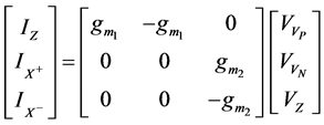 (1)
(1)
The CMOS realization of VDTA is shown in Figure 2 with,
 (2a)
(2a)
 or
or  (2b)
(2b)
where gi is the called as the Transconductance value of ith transistor defined by
 (3)
(3)
3. Basic Wave Equivalent Using VDTA
3.1. Basic Wave Equivalent
For defining the practicality of the filter the wave method is used and defined by the scattering matrix S. The incident and reflected voltage waves are illustrated as Ai and Bi respectively for two port network of Figure 3 and are related by the following relation:
 (4)
(4)

Figure 1. Symbol of VDTA.

Figure 2. CMOS implementation of VDTA [7] .

Figure 3. Incident waves A1, A2 and reflected waves B1, B2 for two port network.
Equation (4) can be expressed in terms of scattering matrix S as
 (5)
(5)
The series inductor L and parallel capacitor C can be described in terms of scattering parameter given by Equation (6) for L and C respectively.
 and
and  (6)
(6)
By going through the concept of wave filtering using the scattering parameter description, the incident waves (Ai) and the reflected waves (Bi) of an inductor (L) in series branch, are expressed as Equations (7) and (8).
 (7)
(7)
 (8)
(8)
where  is time constant and R is the characteristic resistance assigned at each port named port resistance [1] [2] . Similarly for a capacitor (C) in shunt branch the equations are (9) and (10) where
 .
.
 (9)
(9)
 (10)
(10)
Equations (7), (8), (9) and (10), can be realized by the use of following processes: 1) Lossy Integration-Subtraction, 2) Subtraction and 3) Summation.
3.2. Lossy Integration-Subtraction
A Lossy integration-subtraction configuration is shown in Figure 4. It uses a single VDTA, a parallel combination of resistor R2 and capacitor Cd at output terminal X+ and also a grounded resistor R1 at output terminal Z.
The input-output relationship is given by the following equation:
 (11)
(11)
where the realized time constant ,
,  and
and . On comparing Equation (11) with equations (7) and (8), it is accomplished that the following condition must be fulfilled:
 . Considering, port resistance R = R2, the value of capacitor in wave active realization is given by:
 (12)
(12)
Subtraction:
To implement the subtraction operation using VDTA, the configuration is depicted in Figure 5.
 (13)
(13)
Summation:
A VDTA based summation configuration is shown in Figure 6. It consists of two VDTAs. The first VDTA

Figure 4. Lossy integration-subtraction using VDTA.

Figure 5. Subtraction using VDTA.

Figure 6. Summation using VDTA.
reverses the input Vin2 which is then subtracted from input Vin1 by second VDTA to give,
 (14)
(14)
Using the blocks in Figure 4, Figure 5 and Figure 6, the resultant wave equivalent of an inductor in seriesbranch as given by Equations (7) and (8) is shown in Figure 7 and its symbolic representation is shown in Figure 8.
Similarly, the resultant wave equivalent of a capacitor in shunt-branch as given by Equations (9) and (10) is shown in Figure 9 and its symbolic representation is shown in Figure 10.
4. Complete Set of Wave Equivalents
According to the wave method, the wave flow diagrams that could be employed for designing active filters are summarized in Table 1. The required inversion blocks could be obtained by employing the subtraction block in Figure 5 with the condition that Vin1 = 0.
To accomplish the construction of whole filter circuit, the main points are: port resistances are assumed to be equal and the cross-cascade connection of the incident and reflected waves is applied because the incident wave at each port equals the reflected wave at the foregoing port [1] -[6] . Wave equivalents are substituted in place of individual capacitors and inductors and the complete structure is then achieved by cascading the respective wave equivalents.
5. Simulation Results
Simulations are performed by using SPICE program with TSMC CMOS 0.18 µm process parameters. The aspect ratios of various transistors used are given in Table 2. Supply voltages are taken as VDD = −VSS = 0.9 V and

Figure 7. VDTA based wave equivalent of an inductor in series branch.

Figure 8. Symbolic representation wave equivalent of series inductor.

Figure 9. VDTA based wave equivalent of a capacitor in parallel branch.

Figure 10. Symbolic representation of wave equivalent of parallel capacitor.
the transconductances of VDTA were controlled by bias currents IB1 = IB2 = IB3 = IB4 = 513.36 uA. Thus, the transconductance were found to be gm1 = gm2 = 1 mA/V. For verification of the suggested method defined in Sections 3 and 4, a 4th order low pass Butterworth filter (Figure 11) has been taken for experiment. The component values used are RS = RL = 1 KΩ, L1 = 0.2437 mH, L2 = 0.5884 mH, C1 = 0.5884 nF, C2 = 0.2437 nF.
The filter circuit is implemented using the wave equivalents of series inductor and parallel capacitor. The theoretically predicted value of cutoff frequency and also measured by the response of 4th order low pass Butterworth filter shown in Figure 12 is 511.48 KHz. The resistors R1, R2 are chosen to be 1 kΩ according to gm1R1 = gm2R2 = 1. The values of capacitor Cd for wave equivalent of series inductors (L1, L2) are 0.12185 nF, 0.294 nF and for wave equivalent of shunt capacitors (C1, C2) are 0.2942 nF, 0.12185 nF. The complete structure obtained by cascading the wave equivalents is shown in Figure 13 and has been simulated using VDTA based wave

Table 1. Wave equivalent of elementary two port consisting of single element.
Table 2. Transistors aspect ratios for VDTA.

Figure 11. 4th order low pass butterworth filter.
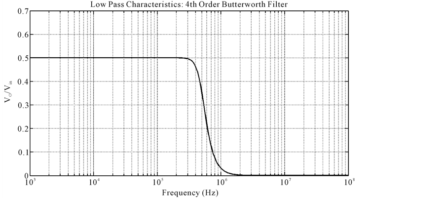
Figure 12. Frequency response of 4th order low pass butterworth filter.
equivalents. Figure 14 and Figure 15 display the simulated filter responses for 4th order low pass (VO) and its complementary high pass (VOC) respectively. The measured cutoff frequency of the filter was 503.52 KHz.
6. Conclusion
A new wave active filter is presented using recently introduced ABB VDTA. VDTAs are used to design lossy integration-subtraction, subtraction and summation blocks, which are the main steps in realizing the wave active filter. The wave method is verified by realizing the 4th order low pass and high pass responses. The proposed wave filter may be designed by using other ABBs which requires lesser power consumption than VDTAs. SPICE

Figure 13. Wave equivalent of 4th order butterworth filter.
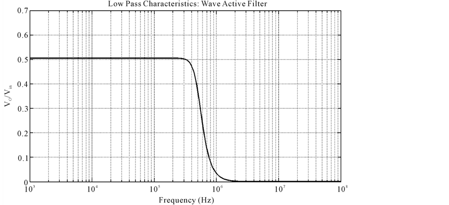
Figure 14. Frequency response of 4th order low pass filter: wave active filter.
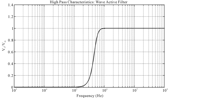
Figure 15. Frequency response of 4th order complementary high pass filter: wave active filter.
simulation results thus confirm the operation of wave active filter with 0.18 µm TSMC CMOS technology parameters.
References
- Wupper, H. and Meerkotter, K. (1975) New Active Filter Synthesis Based on Scattering Parameters. IEEE Transactions on Circuits and Systems, 22, 594-602. http://dx.doi.org/10.1109/TCS.1975.1084089
- Haritantis, I., Constantinides, A. and Deliyannis, T. (1976) Wave Active Filters. IEE Proceedings, 123, 676-682.
- Koukiou, G. and Psychalinos, C. (2010) Modular Filter Structures Using Current Feedback Operational Amplifiers. Radioengineering, 19, 662-666.
- Pandey, N. and Kumar, P. (2011) Differential Voltage Current Conveyer Transconductance Amplifier Based Wave Active Filter. Journal of Electronic Devices, 10, 429-432.
- Pandey, N., Kumar, P. and Choudhary, J. (2013) Current Controlled Differential Difference Current Conveyor Transconductance Amplifier and Its Applications. ISRN Electronics, 2013, Article ID: 968749.
- Bothra, M., Pandey, R., Pandey, N. and Paul, S.K. (2013) Operational Trans-Resistance Amplifier Based Tunable Wave Active Filter. Radioengineering, 22, 159-166.
- Yesil, A., Kacar, F. and Kuntman, H. (2011) New Simple CMOS Realization of Voltage Differencing Transconductance Amplifier and Its RF Filter Application. Radioengineering, 20, 632-637.
- Prasad, D. and Bhaskar, D.R. (2012) Electronically Controllable Explicit Current Output Sinusoidal Oscillator Employing Single VDTA. ISRN Electronics (USA), 2012, Article ID: 382560.
- Prasad, D. and Bhaskar, D.R. (2012) Grounded and Floating Inductance Simulation Circuits Using VDTAs. Circuits and Systems (USA), 3, 342-347. http://dx.doi.org/10.4236/cs.2012.34048
- Prasad, D., Bhaskar, D.R. and Srivatava, M. (2013) Universal Current-Mode Biquad Filter Using a VDTA. Circuits and Systems (USA), 4, 29-33. http://dx.doi.org/10.4236/cs.2013.41006
- Prasad, D., Srivatava, M. and Bhaskar, D.R. (2013) Electronically Controllable Fully-Uncoupled Explicit CurrentMode Quadrature Oscillator Using VDTAs and Grounded Capacitors. Circuits and Systems (USA), 4, 169-172. http://dx.doi.org/10.4236/cs.2013.42023
NOTES

*Corresponding author.