Circuits and Systems
Vol.4 No.5(2013), Article ID:36470,8 pages DOI:10.4236/cs.2013.45052
Design and Verification of a High Performance LED Driver with an Efficient Current Sensing Architecture*
1Peking University, Shenzhen SOC Key Laboratory, PKU HKUST Shenzhen Institution, Shenzhen Institute of Peking University, Shenzhen, China
2Shenzhen Huayue Terascale Chip Ltd. Co., Shenzhen, China
3Department of Electrical and Electronic Engineering, The Hong Kong University of Science and Technology, Clear Water Bay, Kowloon, China
Email: frankhe@pku.edu.cn
Copyright © 2013 Jin He et al. This is an open access article distributed under the Creative Commons Attribution License, which permits unrestricted use, distribution, and reproduction in any medium, provided the original work is properly cited.
Received January 10, 2013; revised February 10, 2013; accepted February 17, 2013
Keywords: LED Driver; Current Sensing; Capacitor Voltage; Feedback; Circuit
ABSTRACT
A high power buck-boost switch-mode LED driver delivering a constant 350 mA with a power efficient current sensing scheme is presented in this paper. The LED current is extracted by differentiating the output capacitor voltage and maintained by a feedback. The circuit has been fabricated in a standard 0.35 μm AMS CMOS process. Measurement results demonstrated a power-conversion efficiency over 90% with a line regulation of 8%/V for input voltage of 3.3 V and current output between 200 mA and 350 mA.
1. Introduction
High-power LED has been widely used as flashlight for camera phones and electric torch for night vision. The most commonly used high-power LED is driven at 350 mA, and LED manufacturers are constantly working on driving LED at higher output current, so that it can provide sufficient light output for broader lighting applications [1]. This brings about the need for high-power LED driver that can deliver and regulate LED-current. Switch Mode Power Converters (SMPCs) are common for high-power LED driver as they can deliver high output-current at high power-conversion efficiency. However, SMPCs are usually output-voltage-regulated, and thus the output current has to be converted to a voltage before it can be regulated. Commercial products use a sensing resistor placed in series with the high-power LED to sense the current directly and convert it to a feedback voltage [2-7]. For applications like flashlights in camera phones or torches where only one high-power LED is used, power dissipation for the sensing circuit can take up more than 20% of the total power delivered [4]. This seriously compromises power-conversion efficiency and shortens battery-life.
As Li-ion batteries with a voltage range from 2.7 V to 4.2 V, it’s commonly used as power source for handheld devices. A high-power LED driver has to step up or step down this supply voltage to drive a 350 mA high-power LED of forward voltage ranging from 3.4 V to 3.7 V. This makes buck-boost converter one of the most suitable candidates. In this paper, an LED-current sensing circuit that is suitable for buck-boost and boost converter is presented. In the following sections, the operation principle and implementation of the proposed LED-current sensing circuit will be presented together with the measurement results.
2. Design of Power Efficient Current Sensing Scheme
The most common approach [2-7] for sensing the LED current is illustrated in Figure 1 with a sensing resistor in series with the LED. In such approach, the power dissipation in the sensing circuit is given by
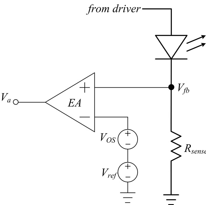
Figure 1. Common LED-current sensing scheme with a current sensing resistor.
 (1)
(1)
Typical reference voltage used is between 110 mV to 1.23 V [1-7] so that Rsense ranges 314 Ohm to 3.5 Ohm. The power consumption can then be estimated to be in the range of 38.5 mW to 430 mW, which is relatively high. An the same time, the power consumption of the sensing circuit increase with the square of output current as given in Equation (1), which is undesirable for high current circuits.
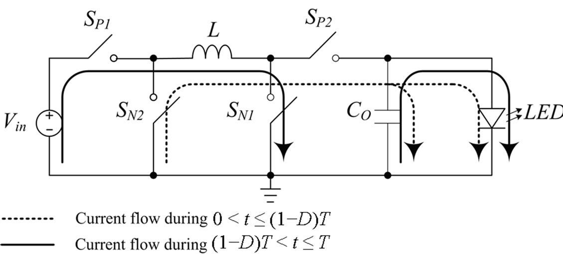
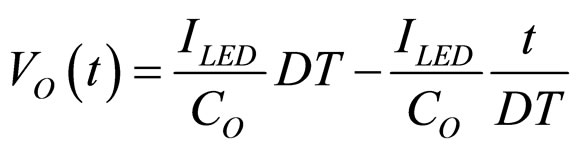
The output current of a buck-boost converter, however, can be directly extracted from the capacitor voltage at the output [8]. Figure 2(a) illustrates a buck-boost converter driving a high-power LED and the waveforms at a few important nodes are sketched in Figure 2(b). In the time interval  (the “reset” state), switches SP1 and SN1 are open and switches SP2 and SN2 are close. The driver is detached from the voltage source Vin. Energy stored in inductor is delivered to output capacitor CO and the high-power LED. In the time interval (1 − D)T < t ≤ T (the “set state”), switches SP1 and SN1 are close and switches SP2 and SN2 are open. Current flows from voltage source Vin to inductor L where the energy is stored. Meanwhile, the high power LED is disconnected from the inductor and output-current is solely provided by output capacitor CO. Therefore, current flowing out of output capacitor is equal to the LED-current in this time period, and this LED-current is equal to the slope of decreasing VO based on equation (2).
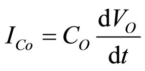 (2)
(2)
By differentiating the output voltage, the current information can be obtained without using a sensing resistor network and thus achieve significant power saving.
3. Circuit Implementation
The overall system of a Buck-boost LED driver with proposed LED-current sensing circuit is shown in Figure 3. The proposed LED driver makes use of leading-edge
 (a)
(a) (b)
(b)
Figure 2. (a) The current path of a buck-boost High-power LED driver at different phase in a period and (b) sketches of waveforms at some important nodes.
modulation in PWM control and is voltage-programmed. Power transistors SP1, SN1 SP2 and, SN2, inductor L and output capacitor CO form the power stage of the Buck-boost LED driver. Resistor Rfb1 and Rfb2 form the resistive feedback network to feedback a portion of the output voltage to the system control. There is a dead time control block to produce a delay between the switching of SP1, SN1 and SP2, SN2 during each switching cycle to prevent shoot-through current in the power stage. There are also drivers to turn on and off the power transistors as they are very large in size. An oscillator OSC is used to generate a ramp and clock signal for both PWM control blocks. A dimming control block is implemented to allow PWM dimming of LED. There is also a start-up current limiting block to limit the power transistor and inductor current during system start up, and a shut-down current limiting block to perform similar function when the system is under dimming operation.
3.1. LED-Current Sensing Circuit
System diagram of the proposed LED-current sensing circuit is shown in Figure 4. The first amplifier, Rdiff and Cdiff form the differentiator to generate Vdiff. Sampling

Figure 3. The system diagram of the proposed buck-boost LED driver.
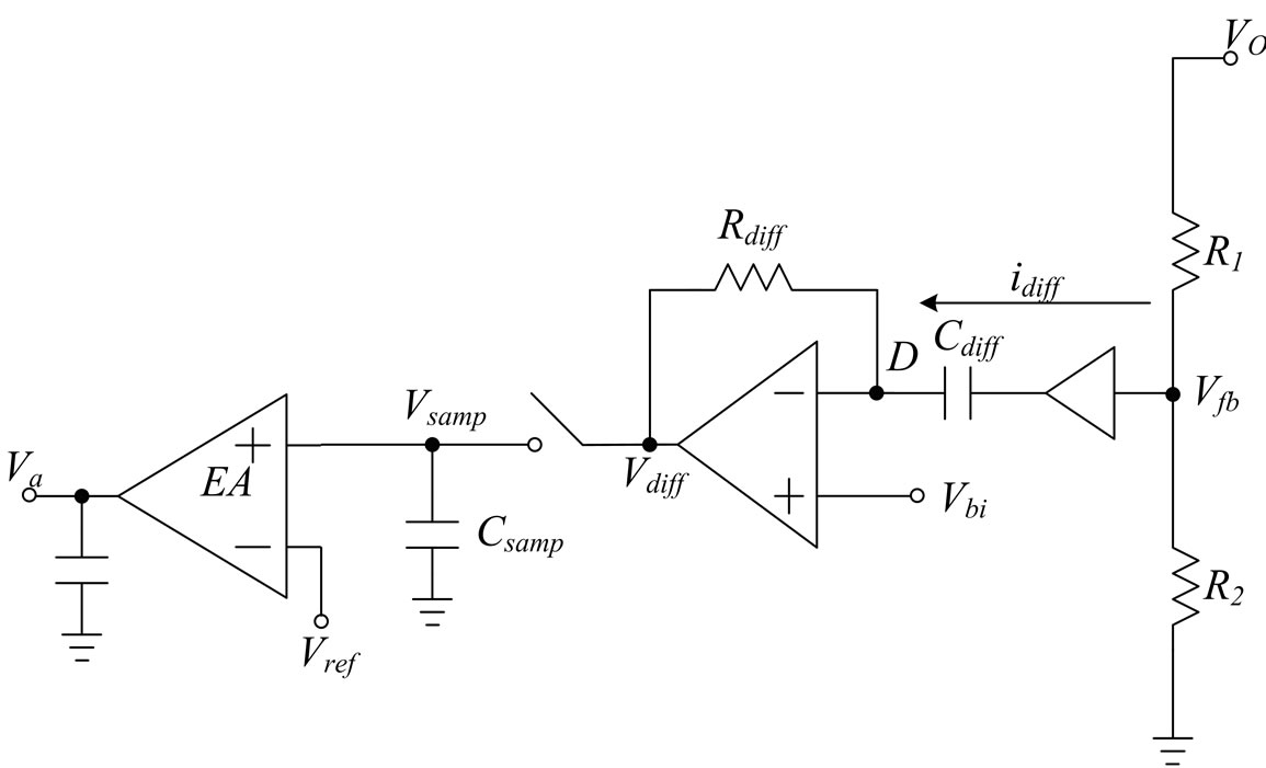
Figure 4. The system diagram of proposed LED-current sensing circuit.
switch and capacitor form the sample and hold circuit that sample the output of the differentiator during the ‘set’ period and hold it for the remaining time. The second error amplifier compares the sampled voltage Vsamp and compare with reference voltage Vref to record the LED-current.
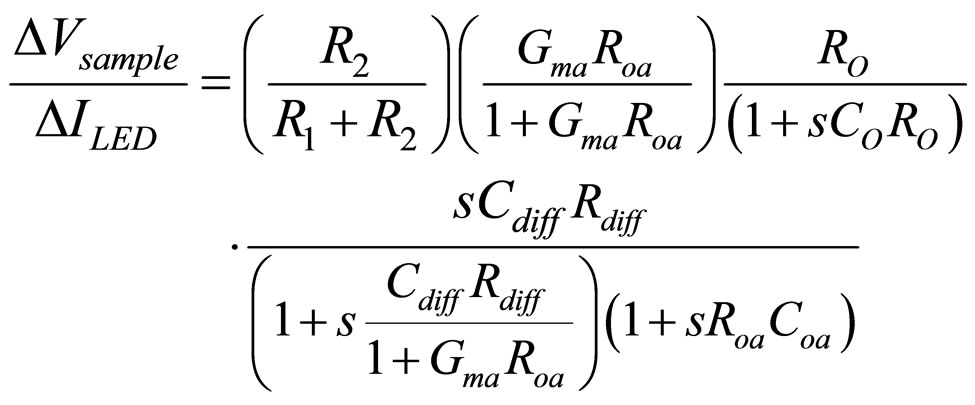
To simplify the analysis, the sampling switch and voltage buffer are assumed to be ideal. The gain of error amplifier is assumed to be GmaRoa and the current drawn by feedback resistor is negligible. The sample voltage of the proposed LED-current sensing circuit during (1 − D)T < t < T is given by:
 (3)
(3)
From Equation (3), the relationship that the sampled DC voltage is proportional to the slope of the capacitor voltage only holds at relatively high frequency such that the “1” in the denominator of (3) become negligible.
Also from the pole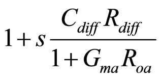 , we can see that the bandwidth of the proposed sensing circuit is limited by the differentiating capacitor, resistor and the gain of the error amplifier. The Bode plot of the proposed LED-current sensing circuit is shown in Figure 5. Such a transfer characteristics between ILED and Vsamp implies that the DC value and slow changes in LED-current is completely filtered out from the system control loop by the differentiator, and thus is not regulated. Intuitively it seems that ILED is not regulated. However, the information of LED-current actually appears in two frequency ranges: 1) the DC value of ILEDRO that is filtered out by the proposed LED-current sensing circuit and 2) the differentiated value of capacitor voltage over time during each switching cycle. It is the second frequency range that is of interested because we are not regulating VO but from the slope of VO that gives the LED-current. The output capacitor has to be chosen carefully in this case such that the cut-off frequency of the LED-current sensing circuit cannot be too low; otherwise, the sampled voltage Vsamp may become output voltage dependent.
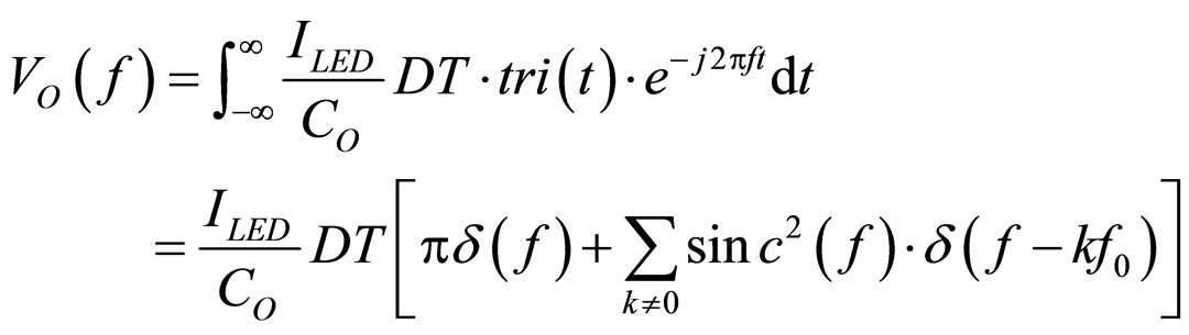
The behavior of the differentiator can be studied by performing Fourier analysis on the output voltage during (1 − D)T < t ≤ T which is assumed to be triangular with the form
 (4)
(4)
The result from the Fourier analysis (on the full triangular wave) is given by
 (5)
(5)
Including all harmonics of the fundamental frequency of the output voltage will require a differentiator with unlimited bandwidth and is not practical. In general, including up to the second harmonics of the signal will be enough [9]. Therefore the bandwidth of the differentiator is designed to be 3 times that of , and thus the maximum required −3 dB bandwidth is about 3.4 MHz. However, to achieve this is very difficult as parasitic poles would appear very close to the dominant pole even for a single stage amplifier. In the proposed LED driver, a current mirror amplifier is used and some gain is traded for stability that results in the transfer function given by Equation (3) and Bode plot in Figure 5. Rdiff = 1.25 MΩ and Cdiff = 4.7 pF have been chosen in our circuit implementation. Transient simulation has been performed and the result shown in Figure 6. In the simulation, a current source is used to simulate the current of SP2 during each switching cycle, which is also the current passed to the LED and output capacitor. It is shown that the differentiator can give reasonably accurate sensing result and Vdiff is about 1.33 V for an LED-current of 350 mA.
As Vdiff is sampled during (1 − D)T < t ≤ T in every switching cycle, the transfer function of the LED-current sensing circuit should not be directly multiplied to the transfer function of the whole converter. The sampling circuit acts as a continuous to discrete converter and at the same time a reconstruction filter that convert the continuous signal Vdiff(t) into a discrete signal and reconstruct it by a zero-order hold interpolation in between each sample [9]. The sampled signal Vsamp[n] can be represented by
 (6)
(6)

Figure 5. Bode plot of proposed LED-current sensing circuit.
As the sampling frequency is equal to the frequency of the differentiator output, Vsamp extracts the output value of the differentiator when (1 − D)T < t < T [9], hence the transfer function of the overall system can be obtained by simply multiplying the conversion ratio between ILED and Vsamp. The resulted transfer function is given by [10]
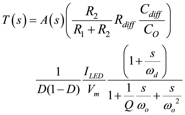 (7)
(7)
3.2. Compensation and System Stability
The proposed LED driver has the same configuration as a

Figure 6. Transient simulation of the differentiator at a fixed load.
typical Buck-boost converter with leading-edge-modulation except for the feedback network. From the transfer function given by Equation (7), a right-half-plane (RHP) zero ωd exists and can be moved to left-half-plane (LHP) when the condition below is fulfilled.
 (8)
(8)
For the proposed design, it is very hard to fulfill such criterion and thus the RHP zero is placed after UnityGain-Frequency (UGF). RHP zero ωd occurs at around 12.4 kHz, and the natural frequency ωo of the LED driver occurs at around 13.3 kHz with Q estimated to be about 1. As the RHP zero locates quite close to the natural frequency, extending bandwidth with a zero is not very effective, hence dominant pole compensation is used to ensure stability.
To achieve the compensation, the transfer function A(s) of the compensation network used should place the UGF of the system at around 1 kHz. A simple differential amplifier and an off-chip compensation capacitor are used to implement the compensation network. The Bode plot of the overall system and that of the power stage alone is shown in Figure 7 indicating reasonable stability has been achieved.
4. Measurement Result
The proposed LED-current sensing scheme is applied to a voltage-mode PWM Buck-boost LED driver and implemented in AMS 0.35 μm process. The chip micrograph is shown in Figure 8 and the area is 2.4 mm by 2.5 mm. Measurements have been performed on sensing accuracy, line and load regulation, and power efficiency of the chip.
In steady state measurement, a supply voltage is 3.6 V and preset output-current is 350 mA. Switching frequency is 1 MHz. Figure 9 shows the waveform of the inductor current and the output current. It can be seen that the driver is stable with the preset output-current. Measured inductor current ripple is 400 mA with an average inductor current of about 600 mA. Measured average output voltage is 3.47 V and the ripple is about 50 mV. The corresponding output current is 350 mA with a ripple current of about 5 mA. Discontinuity in output voltage waveform between the two states in switching cycles indicates that there is a parasitic resistance in series to the output capacitor. When inductor current ramps up, current is drawn from output capacitor to the load leading to a drop in output voltage. On the other hand, when inductor current ramps down to charge up output capacitor, there is a sudden jump in output voltage. There are also spikes during switching instants, which is originated from the switching noise coupled from switching nodes to output node through parasitic capacitances of power MOSFETs.
Figure 10 shows the buffered output of differentiator Vdiff and the buffered sampled voltage Vsamp with a supply voltage is 3.6 V. Because of the switching noise coupled from switching nodes of the driver, there is distortion in the waveform of Vdiff. However, as the value of Vdiff is sampled in instants when the driver is not switching, and the value is held constant thereafter, the switching noise induced distortion that appears in Vdiff is not passed to Vsamp, as shown in the figure. The measured Vsamp is 1.39V for an output current of 350 mA.
A plot of output-current for different reference voltages Vref is shown in Figure 11. The measured feedback

Figure 7. Bode plot of the power stage and overall system of the proposed Buck-boost LED driver.
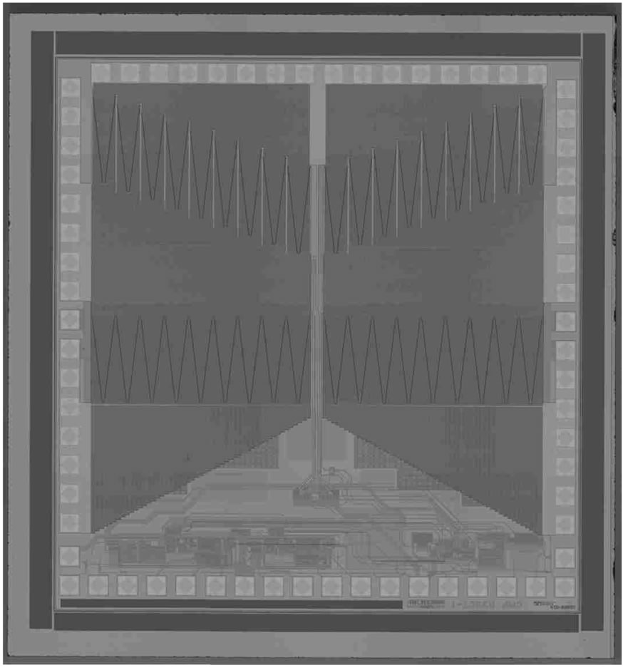
Figure 8. Micrograph of the Buck-boost LED driver with proposed LED-current sensing circuit.

Figure 9. Measured inductor current (top) and output voltage ripple (bottom) at 3.6 V VDD.
factor  is 1.85 mV/mA. When supply voltage Vin is changed from 2.7 V to 3.6 V, the output current for the same reference voltage Vref does not change significantly.
The output current of the circuit is also measured in response to line variation and load variation. As the actual resistance of the high power LED depends on the manufacturing company, two resistors of 10 Ω and 4.7Ω are used. The preset output current is 350 mA, and input voltage VDD is swept from 2.7 V to 3.6 V. Measurement result is shown in Figure 12 indicating that the driver provides a relatively constant output current under different loading resistance. The maximum difference in output current between the two resistance values is 6 mA, which occurs at an input voltage of 3.2 V. For line regulation, the driver provides a relatively constant output current under different supply voltages and the line regu-
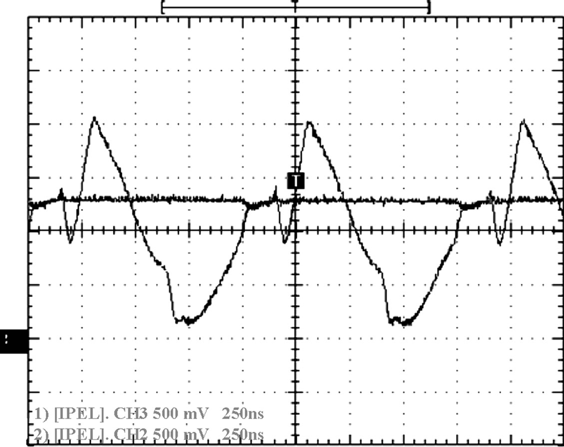
Figure 10. The buffered differentiator output and the sampled voltage of the system with 3.6 V VDD.

Figure 11. Output current versus reference voltage at VDD = 2.7 V and 3.6 V.
lation measured is below 30 mA/V.
Figure 13 shows the efficiency of the driver at 250 mA and 350 mA output current under different supply voltages. The loading resistor used is 10 Ω for both cases. The minimum efficiency is 87%, and is measured at an input voltage of 2.7 V and an output current of 350 mA. The maximum efficiency for 350 mA output current is 92% and is measured at supply voltage of 3.6 V. It can be observed that efficiency is increasing with input voltage. When input voltage increases, average inductor current decreases for the same output, and so thus the conduction loss. It can be interpreted that the main loss of the converter at 350 mA output is the conduction loss. For 250 mA output current, the efficiency is relatively constant and ranges between 90% - 91%. The output voltage for a 250 mA load is about 2.5 V, and the LED driver is in step-down operation for the entire input range. The inductor current is lower compared to the case of
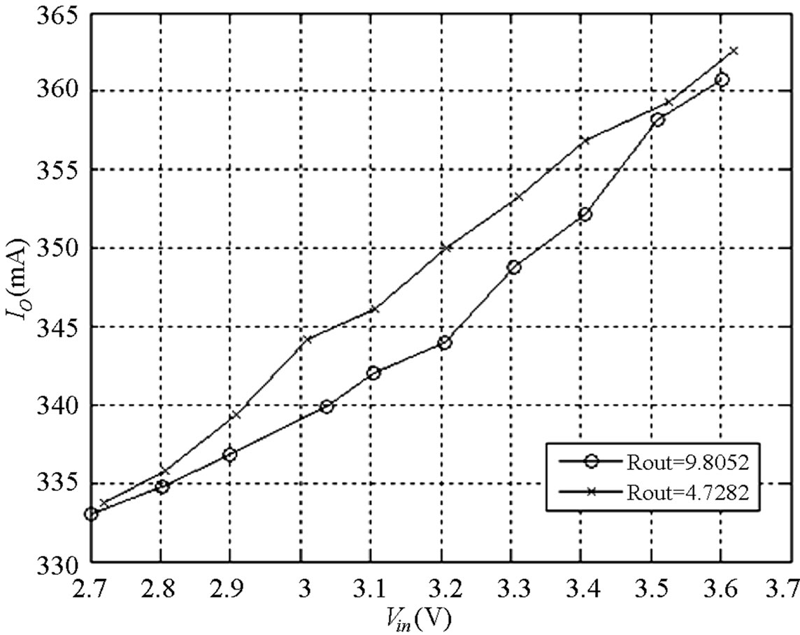
Figure 12. Measured current regulation with different loading resistor values and input voltages.
350 mA output current, hence efficiency is not very seriously degraded even when input voltage is close to its minimum value.
Figure 14 shows the efficiency for output current between 150 mA to 250 mA. Three curves are obtained with input voltages at 2.7 V, 3.3 V and 3.6 V. It can be observed that efficiency first increases and then decreases when the output current increases. At low output current, switching loss is dominant and it is relatively independent of the output conditions. Therefore, efficiency is low at low output power because the same amount of power is used to convert the input power to the output power. When the output power and the output current increases, the efficiency also increases. When the output current increases further, the efficiency is dominated by conduction loss and thus decreases with the output current. We can see from the figure that for an input voltage of 2.7 V, the efficiency is the highest when the output current is about 200 mA. The highest efficiency can be obtained with an output current of 300 mA for Vin = 3.3 V or 350 mA for Vin = 3.6 V. When the output current is low, the efficiency is lower for high input voltage due to the increase of switching loss with increasing input voltage.
5. Conclusion
In this paper, an LED-current sensing circuit that consumes minimal power is proposed. The proposed sensing circuit senses LED-current by differentiating the voltage of the output capacitor and consumes less than 420 μW power. It is implemented in a Buck-boost LED driver and the design is fabricated in AMS 0.35 μm process. Measurement results confirm a reasonable sensing accuracy and line/load regulation. The maximum power efficiency is measured to be 92%. As the power consumption of the proposed LED-current sensing circuit does not

Figure 13. Measured efficiency at different supply voltages.
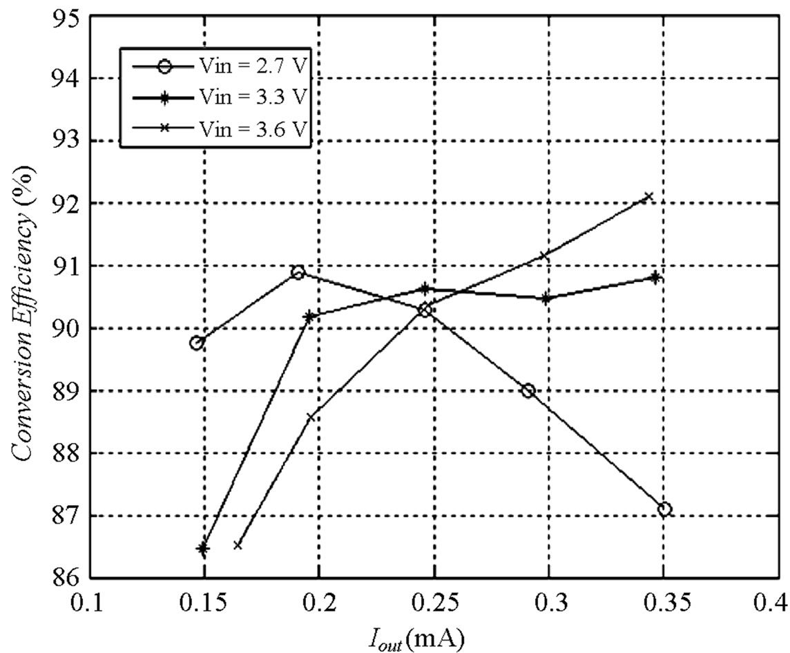
Figure 14. Measured efficiency at different output currents and supply voltages.
increase proportionally with the LED-current, the circuit is particularly useful when LED-current continues to increase in the future.
6. Acknowledgements
This work is supported by Industry Education and Research Foundation of PKU-HKUST Shenzhen-Hongkong Institution (sgxcy-hzjj-201204), by the Guangdong Natural Science Foundation (S2011040001822) and the Fundamental Research Project of Shenzhen Science & Technology Foundation (JCYC20120618163025041). This work is also supported by the National natural Science Funds of China (61204033, 61204043).
REFERENCES
- Philips Lumileds Lighting Company, “Philips Lumileds LED Technology Breakthrough Fundamentally Solves Efficiency Losses at High Drive Currents,” Press Information, Philips Lumileds Lighting Company, San Jose, 2007.
- Linear Technology Corporation, “1A Synchronous BuckBoost High Current LED Driver,” Datasheet LTC3454, Linear Technology Corporation, Milpitas, 2005.
- Maxim Integrated Products, “Offline and DC-DC PWM Controllers for High Brightness LED Drivers,” Datasheet MAX 16802, Maxim Integrated Products, San Jose, 2006.
- LLC, “NCP5030: Buckboost Converter to Drive a Single LED from 1 Li-Ion or 3 Alkaline Batteries,” Datasheet NCP 5030, Rev. 0, Semiconductor Components Industries, LLC, Denver, 2006.
- Maxim Integrated Products, “1.5MHz, 30A, High-Efficiency LED-Driver with Rapid Current Pulsing,” Datasheet MAX 16818, Maxim Integrated Products, San Jose, 2006.
- Texas Instrument Incorporated, “Synchronous Boost Converter with Down Mode High Power White LED Driver,” Datasheet tps61058/tps61059, Texas Instrument Incorporated, Dallas, December 2005.
- National Semiconductor, “1.2A High Power White LED Driver, 2MHz Synchronous Boost Conveter with I2C Compatible Interface, Constant Current Buck Regulator for Driving High Power LEDs,” Datasheet LM 3402, National Semiconductor, Santa Clara, 2006.
- W. Y. Leung, T. Y. Man and M. Chan, “A High-PowerLED Driver with Power-Efficient LED-Current Sensing Circuit,” 2008 European Solid-State Circuits Conference, Edinburgh, 15-19 September 2008, pp. 354-357.
- McClelland, Schafer and Yoder, “Signal Processing First,” Prentice Hall Inc., New Jersay, 2003, pp.71-79.
- W. H. Ki, “Signal Flow Graph in Loopgain Analysis of DC-DC PWM CCM Switching Converters,” IEEE Transactions on Circuit and System I: Fundamental Theory and Applications, Vol. 45, No. 6, 1998, pp. 664-655.
NOTES
*This is an extended version of “A High-Power-LED Driver with Power-Efficient LED-Current Sensing Circuit”, Proceeding of SolidState Circuits Conference, 2008, ESSCIRC 2008, 34th European, pp. 354-357, DOI:10.1109/ESSCIRC.2008.4681865.
More content refers to Wing Yan Leung’s graduated thesis from Department of Electronic and Computer Engineering., Hong Kong University of Science and Technology.