Circuits and Systems
Vol. 4 No. 2 (2013) , Article ID: 29847 , 10 pages DOI:10.4236/cs.2013.42019
Design of Secure Microsystems Using Current-to-Data Dependency Analysis
1The Edwards S. Rogers Sr. Department of Electrical and Computer Engineering, University of Toronto, Toronto, Canada
2School of Engineering, University of Guelph, Guelph, Canada
Email: haleh.vahedi@utoronto.ca, rmuresan@uoguelph.ca, sgregori@uoguelph.ca
Copyright © 2013 Haleh Vahedi et al. This is an open access article distributed under the Creative Commons Attribution License, which permits unrestricted use, distribution, and reproduction in any medium, provided the original work is properly cited.
Received February 24, 2012; revised December 26, 2012; accepted January 3, 2013
Keywords: Secure Microsystems; Differential Power Analysis Attack; Countermeasure; Current Flattening Circuit
ABSTRACT
This paper presents a method for designing a class of countermeasures for DPA attacks based on attenuation of current variations. In this class of countermeasures, designers aim at decreasing the dynamic current variations to reduce the information that can be extracted from the current consumption of secure microsystems. The proposed method is based on a novel formula that calculates the number of current traces required for a successful DPA attack using the characteristics of the microsystem current signal and the external noise of the measurement setup. The different stages of the proposed method are illustrated through designing an example current flattening circuit. Meanwhile validity and applicability of the proposed formula is verified by comparing theoretical results with those obtained experimentally for the example circuit. The proposed formula not only estimates the required level of attenuation for a target level of robustness defined by design requirements, it also predicts the effectiveness of a countermeasure using simulation results therefore dramatically reducing the time to design of secure microsystems.
1. Introduction
Microsystems such as smart cards are at the heart of applications where security is a major concern. In secure microsystems, generally the secret key cannot be accessed directly because of its embedded nature, however, it can be revealed through side-channel attacks that use information extracted from the physical implementation. The most effective side-channel attacks are differential power analysis (DPA) attacks, which use statistical analyses for extracting information from variations of the power-supply current of a cryptographic device [1].
Countermeasures against DPA attacks [2-4] are either software-based or hardware-based, which, in turn, are based on circuit-level or system-level solutions [5]. Typically, system-level solutions assume that attenuating the variations of the power-supply current makes DPA attacks more difficult [5-7]. The number of current traces required for a successful DPA attack (hereafter NCTDPA) is used to evaluate the robustness of a secure microsystem against DPA attacks or the effectiveness of a countermeasure. In the existing literature, such number of traces is found experimentally by running DPA attacks on an increasing number of current traces and repeating the process until the attack is successful.
In this paper a formula is introduced for calculating NCT-DPA of secure microsystems. Here, the NCT-DPA is presented by the characteristics of the current variations of the microsystem while executing a cryptography algorithm and the external noise of the current measurement setup in DPA attacks (i.e. the ac rms value of these two signals). In [8] (p. 54), a formula has been extracted that shows the relationship of the signal to noise ratio, SNR, and NCT-DPA. However, there is an unspecified parameter in the formula (related to the algorithmic noise). Also in [9] (p. 147), a formula has been suggested for the relationship between the SNR and NCT-DPA. In this paper, there will be a cross check between our formula and the relationship suggested by authors of [9].
The proposed formula is used to develop a method for designing countermeasures that aim at attenuating dynamic current variations of microsystems. The resulting method has two main benefits: 1) it allows designers to estimate the required level of current attenuation for a certain level of protection, therefore it can be used as a starting point of design for any countermeasure based on the current variations reduction; 2) it can be used for assessing the robustness of countermeasures in the simulation stage therefore significantly reducing the time to design of secure microsystems.
The remainder of this paper is organized as follows: Section II focuses on deriving the formula for calculating NCT-DPA. In Section III, the attenuation level is estimated by using a specific countermeasure requirement. Section IV briefly discusses a countermeasure circuit as an example for validation of the method. In Section V, the robustness of the proposed design and the credibility of the proposed formula are demonstrated. Section VI discusses the effect of noise on the efficiency of the example circuit and shows the role of the proposed formula in revealing the efficiency of the circuit in conditions where experimental methods are not possible. Concluding remarks appear in Section VII.
2. Deriving a Formula for Calculating NCT-DPA
In a ciphertext-based DPA attack targeting a data encryption standard (DES) algorithm, for each guessed sub-key, e.g. the n-th sub-key, the collected current traces are partitioned into two groups G1 and G0 (using the target bit of a given selection function D). The averages of the partitioned current traces are calculated and their difference gives the differential current trace
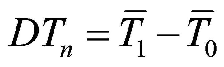 , (1)
, (1)
where  and
and  are the averages of the current traces partitioned in groups G1 and G0 respectively. For example, if a 6-bit sub-key of a DES encryption is chosen, there are 64 possible sub-key guesses, which form a set of differential current traces
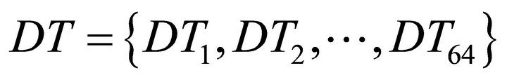 . The correct guessed sub-key is the one that corresponds to the differential trace with the maximum peak [1].
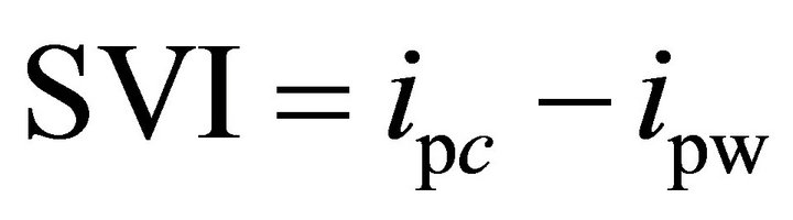
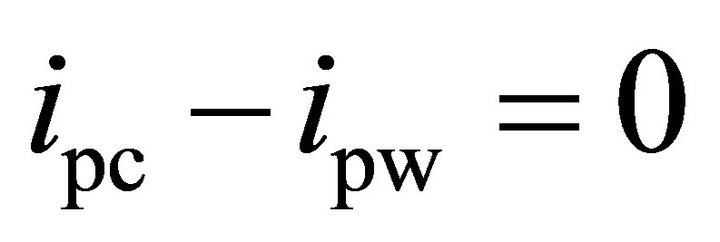
As a figure of merit for evaluating the robustness of a cryptographic device, the difference between the maximum peak of the differential trace for the correct key (ipc) and the maximum peak appearing on the differential traces for the wrong keys (ipw) is called success value indicator [10]
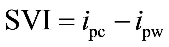 . (2)
. (2)
In a DPA attack with a small number of current traces, some spikes of differential traces corresponding to wrong sub-keys may be higher than the spike of the differential trace for the right sub-key; in this case SVI < 0 and the correct sub-key cannot be guessed. By increasing the number of current traces, the spike of the trace corresponding to the right sub-key increases and those corresponding to wrong sub-keys decrease and eventually, when SVI > 0, the right sub-key can be guessed correctly. The minimum number of traces NCT-DPA for which the value of the maximum peak of the differential trace corresponding to the right sub-key is equal to the highest peak value of the differential traces corresponding to wrong sub-keys gives a quantitative indication of the time required by a DPA attack to be successful.
Obviously, in order to identify the correct sub-key with acceptable confidence, the spike in the differential trace for the correct sub-key must be bigger than the spikes in the differential traces for the wrong sub-keys. To quantify how much bigger it should be, the probability distributions of the spikes and their dependency on electric noise have to be considered.
The sources of noise are modelled as algorithmic and non-algorithmic [8] (p. 53). The algorithmic noise depends on the type of DPA attack being executed and on the number of bits exploited [8] (p. 57), [9] (p. 75). The non-algorithmic noise includes external noise, intrinsic noise, and quantization noise. The external noise is generated by power supply, clock generator, and interference with other parts of a microsystem [9] (p. 55). The intrinsic noise is due to the fundamental properties of electronic devices and it includes thermal, shot, and flicker noise. The quantization noise depends on the quality of the analog-to-digital converter used for sampling the current traces. The dominant non-algorithmic noise is typically the external noise since intrinsic noise is controlled at the design stage and quantization noise is minimized with an appropriate measurement setup [9].
The deviation of the spikes of the differential traces for wrong sub-keys is mainly due to external noise, which can be modelled with a normal distribution [9] (p. 65). The deviation of the spikes of the differential traces for the correct sub-key is mainly due to external noise and algorithmic noise. The algorithmic noise depends on the probability distribution of data, which is binomial and can be modelled as a normal distribution for large number of events. Since algorithmic noise and external noise are independent, their variances can be added up. Figure 1 represents the spike of the differential trace corresponding to the correct sub-key, ipc, and the maximum spike of the differential traces for wrong sub-keys, ipw,
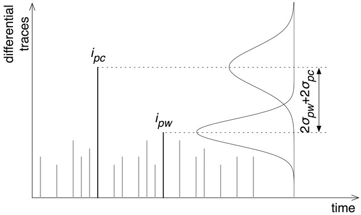
Figure 1. Probability distributions of the spikes of differential traces for the correct sub-key and for wrong sub-keys.
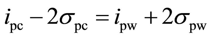
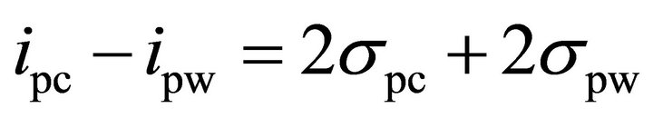
and their distributions. The confidence on revealing the correct sub-key depends on the spacing of the two distributions. As an example, assuming that the standard deviation of the spike of the correct key is much larger than the standard deviation of the spike of the wrong keys are the same, i.e.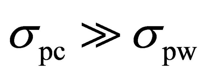 , if the difference of the two mean values is
 (3)
(3)
then the probability of revealing the correct sub-key is over 97%.
If a DPA attack is run for N number of traces, when N is large enough, one can assume that for half of these traces the target bit of the selection function D is equal to 1 and for the other half the target bit is equal to zero. Therefore, if 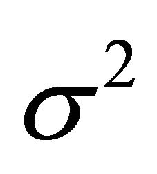 is the variance of a current trace, the variance of each group of
 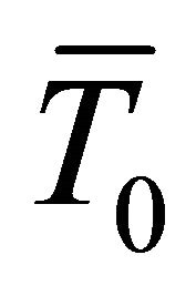 and
and 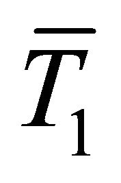 is approximated to
  and the variance of the differential trace will be the sum of the variances of these two independent groupsthat is
  [8] (p. 55). Therefore, (3) can be rewritten as:
 . (4)
. (4)
As mentioned earlier, the variance of the spike of the correct key is due to the external noise and the algorithmic noise (which are independent) and the variance of the spike of the wrong keys is due to the external noise. Therefore:
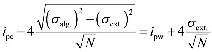 (5)
(5)
where  and
and  are the standard deviations of the algorithmic noise and the external noise, respectively.
The values in (5) should be related to the characteristics of the current traces and noise. Comparing the rms value of the population of x with N samples, 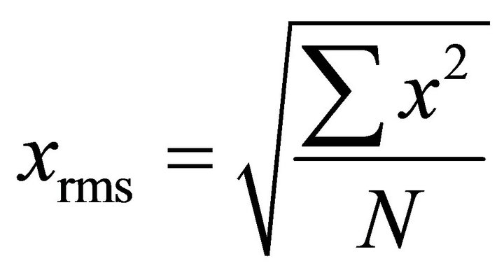 , with the standard deviation of the population x with the mean value µ,
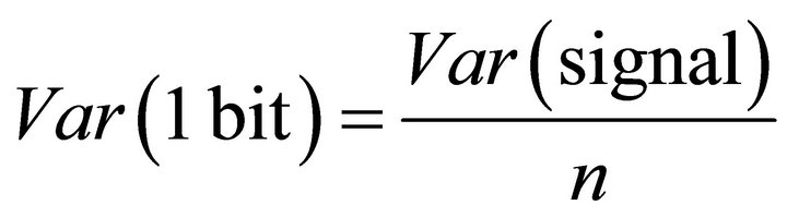
 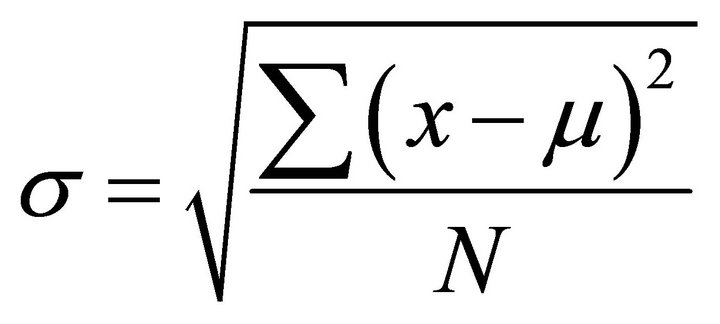 shows that if the mean value is zero, then the rms value and the standard deviation are the same. In other words, the standard deviation is obtained by removing the DC component and measuring the ac rms value. This property is used to measure the standard deviation of the algorithmic noise and the external noise. If in the cryptographic algorithm an n-bit word is processed and the number of collected current traces are large enough, it can be assumed that the deviation of the microsystem current signal is due to n bit transitions. In DPA attacks, if the changes of m bits are exploited, the changes of the remaining n − m bits are considered the algorithmic noise. Therefore, the variance of the algorithmic noise is (n − m)/n times of the variance of the current signal. If the variance is expressed in terms of the standard deviation, and hence in terms of the ac rms value, (5) can be rewritten as:
 (6)
(6)
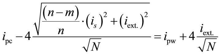
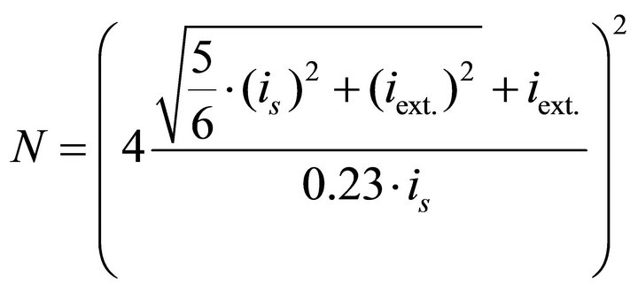
where is and iext. are the ac rms values of the microsystem current signal and the external noise respectively. The required number of traces, N, can be derived by solving (6) to obtain:
 . (7)
. (7)
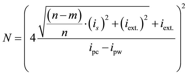
For the DPA attack used in this research, the variations of one bit of a 6-bit word are exploited. Hence, (7) reduces to:
 . (8)
. (8)
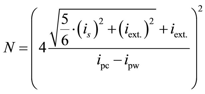
Assuming that the ipc – ipw term is proportional to the rms value of the microsystem current signal (see Section V-B), (8) can be rewritten as:
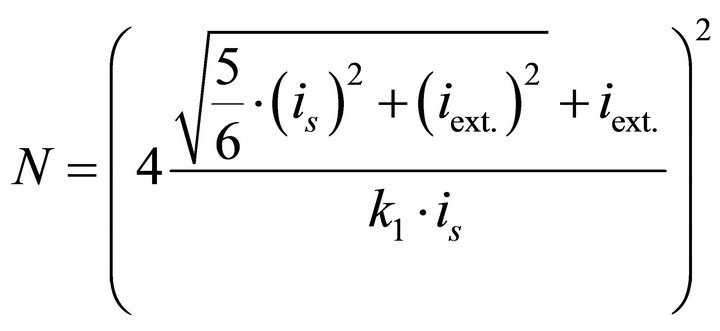 (9)
(9)
where k1, is and iext. are parameters determined by the characteristics of the current signal of a microsystem and the DPA attack measurement setup. In this paper we use (9) to estimate the required level of attenuation for obtaining a certain level of robustness (expressed in terms of NCT-DPA) for a specific microsystem. To that end, we should measure iext. and k1 for the microsystem. Finding k1 requires measuring NCT-DPA for the unprotected microsystem. Finding iext., requires measuring the external noise of the DPA attack measurement setup. The following sub-sections will discuss these measurements.
2.1. Measurement of NCT-DPA for a Specific Unprotected Microsystem
First a set of current traces were measured at the supply pin of an unprotected microsystem while the microsystem was executing DES encryptions. The chosen microsystem device was an 8-bit AVR microcontroller (ATmega16, from ATMEL) operating at 4 MHz clock frequency with a 3.3-V power supply voltage [11]. This is a typical microcontroller used in smart card applications. While the ATmega16 microcontroller was executing DES encryptions on randomly generated plaintexts, 1000 current traces of the microcontroller were collected at the supply pin. The setup for the measurement is shown in Figure 2. It consists of a resistor (R), high frequency differential probes, a signal generator for providing the clock signal, a high-precision power supply, and a highspeed digital sampling oscilloscope for collecting the current traces.
A ciphertext-based DPA attack for a DES algorithm [1] was performed over the collected current traces. For the unprotected microcontroller, the correct sub-key was revealed within 400 traces. This result was obtained by measuring the Success Value Indicator (SVI). Figure 3 shows the SVI graph for DPA attacks with different number of current traces. When SVI (on y axis) is less than zero, the peak value of the differential trace of the correct sub-key is less than the peak value of the differential traces corresponding to the remaining sub-keys; hence, the correct sub-key can not be distinguished. As shown in Figure 3, for the number of traces less than 400, SVI is less than zero. When the number of traces is
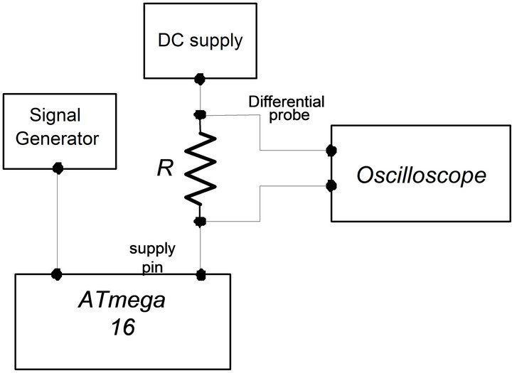
Figure 2. Setup for measuring the current consumption of ATmega16 microcontroller.
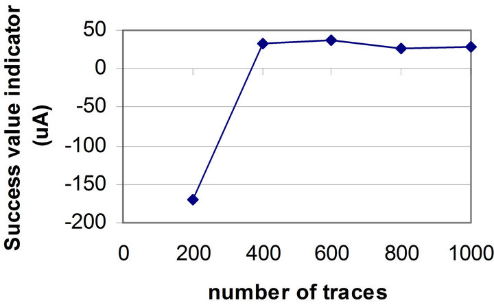
Figure 3. SVI versus the number of current traces for the unprotected microcontroller.
greater than 400, SVI is greater than zero and the correct sub-key may be revealed. This number will be used later for calculating k1.
2.2. Measurement of the External Noise of the Microcontroller Setup
In order to find out the characteristics of the external noise influencing the setup, a DES algorithm was executed over a fixed plaintext for 1000 times. Since the operation and the data were not changed, one would expect that the collected current traces would remain the same. However, because of the external noise, the current traces were not exactly the same. The mean of these 1000 traces was measured and then the external noise was obtained by subtracting the mean from one of the signals. This experiment was performed 5 times and the least noise was chosen. Figure 4" target="_self"> Figure 4 shows the external noise and the mean of the current traces. The rms value of the external noise was 2.015 × 10⁻⁴ A and the rms value of the current signal was 8.5 × 10⁻⁴ A.
2.3. Deriving k1 for the ATmega Microcontroller
By substituting N, is and iext. (from previous sub-sections) into (9), we obtain k1:
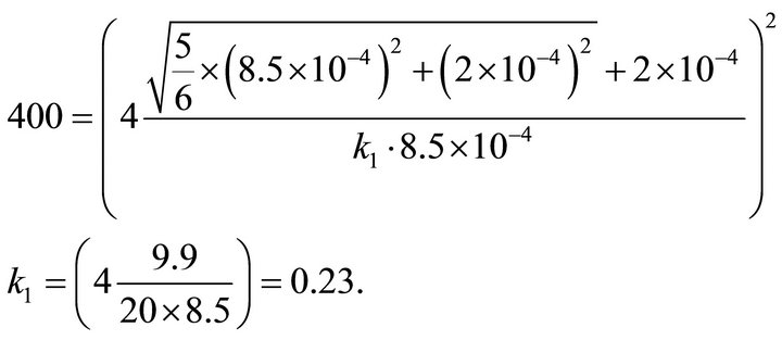 (10)
(10)
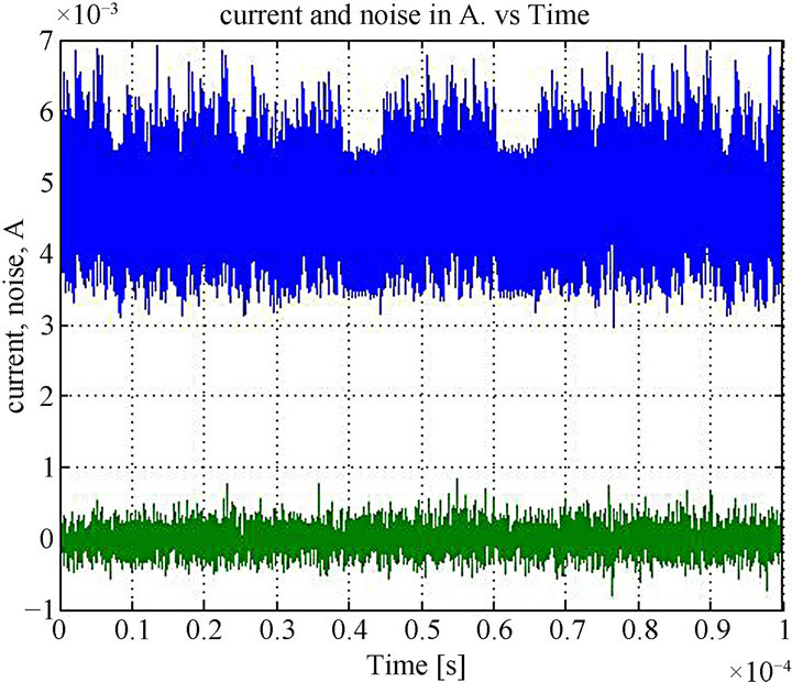
Figure 4. The mean of the ATmega current trace and the external noise of the setup used for collecting current traces of ATmega microcontroller.
By substituting this value of k1 in (9), a formula is obtained for NCT-DPA that is only based on the ac rms values of the current signal and the external noise (for ATmega16).
 . (11)
This formula can be derived for any type of microsystems and will be used as a starting-point of a design methodology discussed in the next sections.
3. Estimating the Required Attenuation Level
As an example, let us consider the design of a countermeasure to protect the ATmega16 microcontroller so that the DPA attack is not successful for less than 10,000 current traces. The rms value of the external noise is assumed to be 2 × 10⁻⁴ A (i.e., the least value of noise seen in the experiment). The required rms value of the current traces can be calculated using (11):
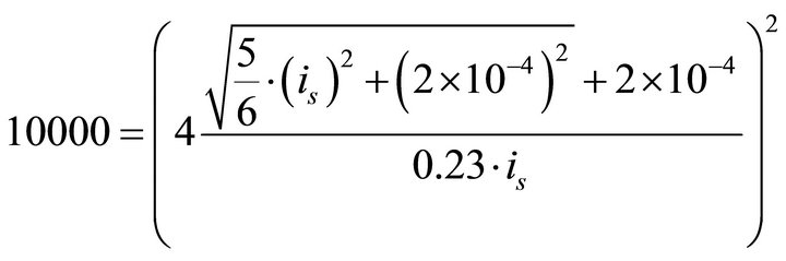 .
.
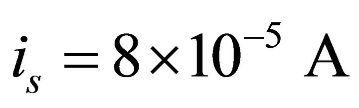 .
.
This current can be translated to a level of attenuation of:
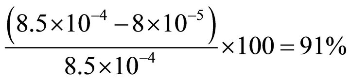
where 8.5 × 10⁻⁴ A is the ac rms value of the current of the unprotected microcontroller while running a DES algorithm.
Having this number in mind, we designed a current flattening circuit that attenuates the dynamic current variations with more than 90% [12]. In the next sections, this example circuit will be introduced briefly, and its efficiency will be investigated and compared with what was expected through the proposed formula (8).
4. Designing a Countermeasure for the Required Level of Attenuation
Figure 5 shows the block diagram of the example circuit. We wish to keep the current through the supply pin (VDD) at a constant level by using a current injection technique.
In Figure 5, the current sensor measures IS at VDD. The output of the sensor,  , an attenuated version of IS, is subtracted from
 , an attenuated version of reference
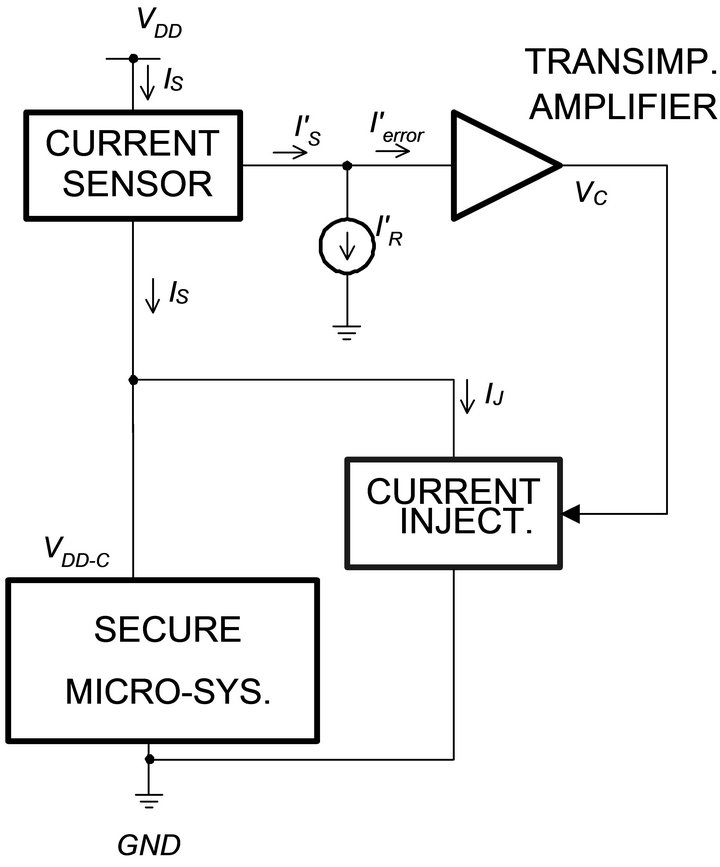
Figure 5. Block diagram of the current flattening circuit.
current (IR); the resultant is fed to a transimpedance amplifier. The output of the amplifier VC controls the current injection block. When IS < IR, this block absorbs an extra current IJ and maintains IS close to IR.
Figure 6 shows the schematic of this circuit. The current sensor is a customized current mirror (M1 and M2) which produces , an attenuated version of the current of the secure microsystem. The current
![]() , the difference between
, the difference between  and
and , is fed to a transimpedance amplifier.
 ![]() is amplified and converted to the voltage VC, the output of the amplifier. This voltage is used for controlling transistor M6, which implements the current injection. This circuit is the design described in [12] and its functionality in reducing the dynamic current variations was verified through extensive simulations and testing the fabricated chip.
is amplified and converted to the voltage VC, the output of the amplifier. This voltage is used for controlling transistor M6, which implements the current injection. This circuit is the design described in [12] and its functionality in reducing the dynamic current variations was verified through extensive simulations and testing the fabricated chip.
5. Investigation of the Robustness of the Example Circuit
To see how robust the example circuit is, NCT-DPA was calculated for different levels of the current attenuation using both the experimental method and the formula (8). This can be considered as a third stage of the design method. In addition, this will be used as a solid experiment for investigating the credibility of the proposed formula.
5.1. NCT-DPA for the Example Circuit
In order to investigate the robustness of the example circuit and also observe the relationship between the current attenuation and NCT-DPA, the current traces collected from the unprotected ATmega16 microcontroller (Section II-A) were imported into the Cadence environment.
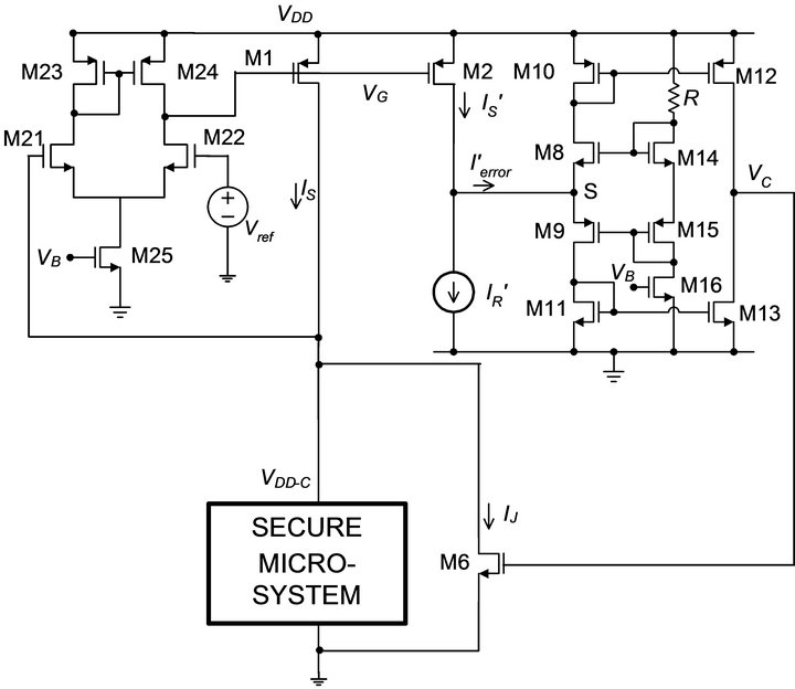
Figure 6. Schematic diagram of the current flattening circuit.
These current traces were applied as the input signal to the current flattening circuit in order to emulate the current variations of a smart card microcontroller performing a DES encryption. Setting the reference input of the current injection loop, the original current traces were flattened with different levels of attenuation. Table 1 summarizes the simulation results. As seen in Table 1, the simulation was run for five different current reference values and five sets of current traces with different level of attenuations were obtained. The attenuation of each set was calculated in terms of the rms value of the current signal.
Next, DPA attacks were run over each set of current traces. Figure 7" target="_self"> Figure 7 and the last column of Table 1 show how the flattened signals with different levels of attenuation responded to a DPA attack. The y axis in Figure 7 is SVI for the DPA attack. One can see that by reducing the ac rms value of the flattened current signal, NCT-DPA increases. When the rms value of the flattened current is 6.3 × 10⁻⁶ A, which is translated to 99.26% attenuation, NCT-DPA reaches 9600.
Since the experiments were performed over the noisefree output of the simulator, our experimental results show different attenuation value compared to the attenuation obtained through the formula in Section III; that is 99.26% attenuation required for a NCT-DPA of 9600 in the experimental method compared to 91% attenuation estimated for a NCT-DPA of 10,000 in the first stage of the design. Repeating the calculation presented in Section III and using (11) with only the attenuated external noise added to the input signal, 4 × 10⁻⁶ A, is will be equal to 1.4 × 10⁻⁶ A. This value can be translated to 99.8% expected attenuation, which is close to what was obtained through the Cadence experiment. Hence the
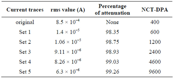
Table 1. Rms value, attenuation, and NCT-DPA for signals with different levels of attenuation.
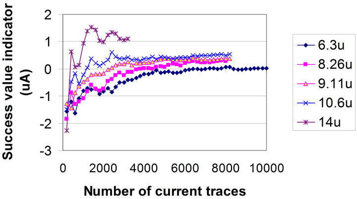
Figure 7. SVI versus number of current traces for flattened currents with different rms values.
validity of the estimation in the previous section is verified.
For verifying the validity of the formula (8), the NCTDPA values for the 5 sets introduced in Table 1 were calculated by using this formula. For this purpose, the spike values of the differential current traces for the correct sub-key and wrong sub-keys were obtained by running a DPA attack with 10,000 traces. The spike values and their corresponding current rms values are shown in Table 2. Since simulation results are used here, the external noise can be considered zero. By substituting the values is, ipc, and ipw from this table into the formula (8), the NCT-DPA is obtained as shown in the 4-th column of Table 2. The NCT-DPA obtained experimentally (Table 1) is repeated in the 5-th column of this table. Comparing these two columns shows that the NCT-DPA obtained through these two methods are very close to each other, which verifies the credibility of (8).
The difference in the last two columns can be quantified by comparing (2) and (3), which are repeated here:
 .
.
 .
.
Decision point for the experimental method is the point where SVI is equal to zero:
 (12)
(12)
and the decision point for the formula is where:
 . (13)
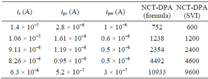
Table 2. NCT-DPA using the formula and the experimental method for the flattened current traces with different rms values.
By comparing (12) and (13), one can see that the difference between the decision points of the two methods is the term  . As discussed in Section II, the deviation of the spike of the correct sub-key is due to the external noise and the algorithmic noise and the deviation of the spikes of the differential traces of the wrong sub-keys is due to the external noise. Since, experimental results are obtained from the simulator output, where the external noise is negligible,
  is zero and
  is mainly determined by the algorithmic noise. Also, the variance, and therefore, the standard deviation of the algorithmic noise, is related to the rms value of the current signal. Since the current signal is flattened and its rms value is reduced significantly, the algorithmic noise is very small and therefore, the term of
  is negligible. This point justifies the similarity of the numbers in the last two columns of Table 2 and demonstrates the validity of (8).
5.2. Verifying the Assumption Made in Deriving (9)
In deriving (9), we assumed that ipc – ipw is proportional to the rms value of the current signal. In order to verify this assumption, the difference between ipc and ipw was drawn versus the rms value of the current signal. As shown in Figure 8, this relationship was contrasted with a linear function and the comparison demonstrated that this relationship is linear and the assumption made in Section II is valid.
The slope of the line in Figure 8 is equal to the parameter k1 in (9). This slope is 0.2 and close to the value of k1 calculated from the DPA characteristics of the unprotected ATmega16 (see (10)).
NCT-DPA obtained in this section for the example circuit was based on simulation results where the external noise was negligible. In the next section, we present more realistic NCT-DPA results by running the experiments considering the external noise.
6. NCT-DPA in the Presence of Noise
In this section the relationship between NCT-DPA and the level of current attenuation in the presence of external
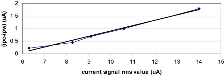
Figure 8. The difference between ipc and ipw versus the rms value of the current signal.
noise is investigated. First, a formula will be derived for the signal to noise ratio in DPA attacks. Then NCT-DPA is examined for a flattened current in the example circuit with a low level of attenuation in the presence of noise.
6.1. Signal to Noise Ratio in DPA Attacks
Signal to noise ratio is defined as the ratio of the power of signal to the power of noise. If Pexp.signal is the part of the power exploited for the DPA attack and Pnoise is the power of the noise, the signal to noise ratio (SNR) is:
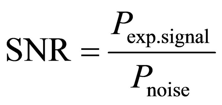 . (14)
Since we are only interested in the dynamic part of the power, the power can be translated to the variance of the signal and SNR becomes:
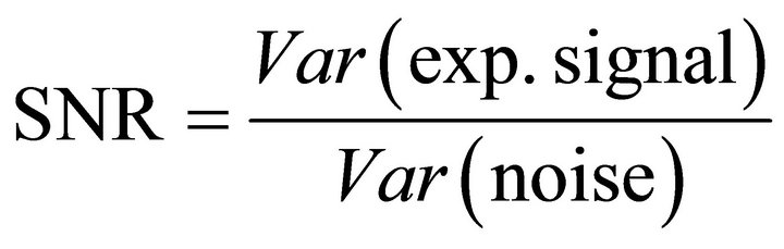 (15)
(15)
where, Var(exp. signal) is the variance of the exploitable signal and Var(noise) is the variance of noise. As mentioned earlier, the main components of noise are the external noise and the algorithmic noise. These two terms are independent and their variances will add up. Hence, (15) can be rewritten as [9] (p. 73):
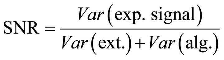 (16)
(16)
where Var(ext.) and Var(alg.) are the variances of the external noise and the algorithmic noise respectively.
We assume that an n-bit word is processed in a cryptographic algorithm and the variance of the current signal is Var(signal). If the number of current traces used for a DPA attack is large enough and the random ciphertext allows the transitions of all n bits of the word, then the deviation of the current signal belongs to n bit transitions. Since the variations of different bits are random and independent, then the variance for each bit can be estimated as:
 . (17)
If the information of the m bits of n-bit word is exploited for breaking the security in a DPA attack, the variance of the exploitable signal can be estimated as:
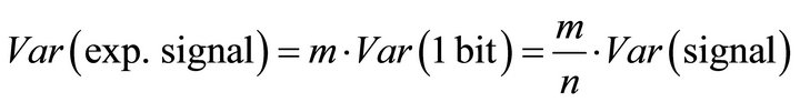 (18)
(18)
The variance of the algorithmic noise, i.e. the variance of the non-exploited bits, is:
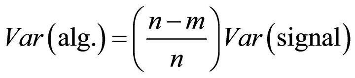 . (19)
Substituting (18) and (19) in (16), we obtain:
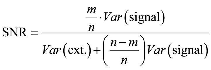 . (20)
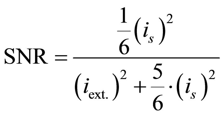
For the DPA attack used in this research, where the variations of 1 bit of the 6-bit word are exploited (i.e. m = 1 and n = 6), the SNR can be estimated as:
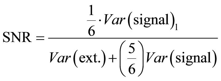 . (21)
6.2. NCT-DPA of the Example Circuit in the Presence of Noise
A set of current traces collected at the supply pin of the ATmega16 microcontroller was imported into the Cadence environment. By applying the current injection feedback, the current traces were flattened. The considered current flattening situation had a flattened current with 79 µA peak-to-peak and 1.4 × 10⁻⁵ A rms value, and 98.35% reduction in rms value (see Table 1).
Running a DPA attack over the output of this flattened current set showed that the DPA attack was successful with less than 600 current traces (Table 1). These traces were collected from the simulator where there was no external noise. In order to see the effect of the external noise on the success of DPA attack on the protected microcontroller (with the current flattening circuit), a set of simulations were run by adding different levels of noise to the output of the simulator. The added noise was a random current noise with the frequency of 8 MHz, i.e., the first harmonic of the clock signal of ATmega16. One should note that most of the power of the external noise is generally concentrated at the clock frequency and its harmonics [9]. DPA attacks were performed and NCTDPA values were derived. The results are shown in Figure 9.
As an alternative to the experimental method, one can calculate NCT-DPA by using (8) along with the characteristics of the flattened current and the noise. For finding the maximum spike values, a DPA attack with a large
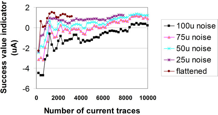
Figure 9. SVI for a flattened current and the combination of the flattened current traces and different levels of noise.
number of traces was run on the flattened current with 1.4 × 10⁻⁵ A ac rms value. When running DPA with 10,000 traces, it was observed that ipc was 2.8 × 10⁻⁶ A and ipw was less than 10−6 A. NCT-DPA was calculated by substituting these values in (8). Table 3" target="_self"> Table 3 shows NCTDPA for different values of noise calculated in two ways: the experimental method and the formula.
Table 3 shows that when noise increases, the values of NCT-DPA calculated from two methods diverge. This is due to the fact that when the standard deviation of noise increases, the term  is not negligible any more (see Section V-A) and SVI no longer shows the accurate number of traces. In this case, more traces are required to remove the ambiguity between the spike of the differential trace of the correct sub-key and those of the wrong sub-keys.
6.3. A Cross-Check of the NCT-DPA Formula with a Previously Developed Relationship
Mangard et al. have calculated NCT-DPA by using a correlation factor and derived a rule of thumb. Their approach suggests that for small SNRs, NCT-DPA is inversely proportional to SNR [9] (p. 147):
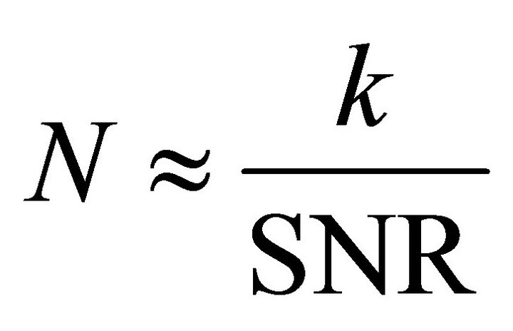 . (22)
In order to compare our derived formula (8), with the relationship suggested by Mangard et al., SNR can be calculated for different values of noise by using (21). Since the ac rms value of the current signal is equivalent to the standard deviation, (21) can be rewritten as:
 . (23)
Using this formula, the inverse of SNR was calculated for different values of noise. The results are shown in Table 4 along with NCT-DPA obtained from two methods. NCT-DPA is drawn versus the inverse of the SNR for both methods in Figure 10.
Figure 10 shows that for the numbers obtained by our
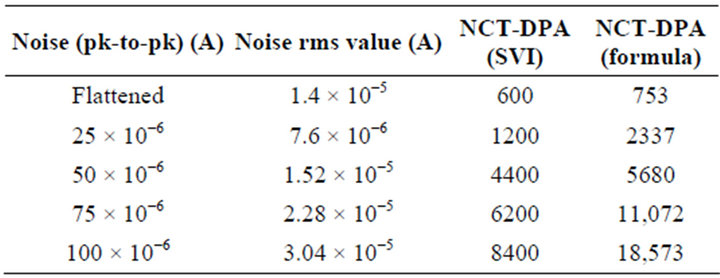
Table 3. NCT-DPA for different levels of noise using the experimental method and the formula.
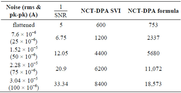
Table 4. The inverse of SNR and NCT-DPA for two methods.
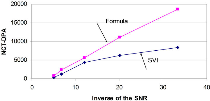
Figure 10. NCT-DPA versus the inverse of SNR.
formula, there is a linear relationship between NCT-DPA and the inverse of SNR as suggested by Mangard et al. (see (22)). This is another evidence for the validity of our formula. For the experimental method when noise increases, the number of current traces obtained does not show a linear relationship with SNR. One may conclude that while SVI is a reliable figure of merit for measuring NCT-DPA in the absence of noise, it does not show the accurate number of traces in the presence of large levels of noise. This confirms the conclusion made at the end of the last sub-section, i.e. the term 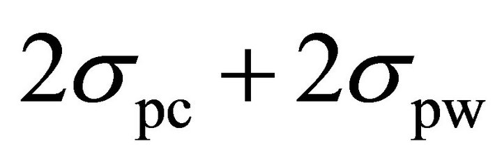 is not negligible any more and the experimental method results are not accurate.
The linear relationship depicted in Figure 10 and suggested by our formula provides an opportunity to find an empirical value for the parameter k in (22). This parameter is the slope of the line in Figure 10:
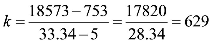 . (24)
We call the parameter k the efficiency gain of the countermeasure. This parameter can be used to estimate the NCT-DPA for the flattened currents with higher levels of attenuations (when the NCT-DPA cannot be obtained experimentally). This application is shown in the next subsection, where NCT-DPA is calculated for the current traces with different levels of attenuation.
6.4. Using Efficiency Gain for Finding NCT-DPA
In this sub-section, NCT-DPA is calculated for several sets of current traces with different levels of attenuations in the presence of the external noise measured for the setup used for collecting current traces of the ATmega16 microcontroller (Section II-C). First, using (23), SNR is calculated for these different sets, considering the measured external noise with the rms value of 2.015 × 10⁻⁴ A (Section II-C). Then using (22) and the efficiency gain k, (24), NCT-DPA is calculated for all these sets. Table 5 summarizes the results for five sets of the flattened current traces introduced in Table 1.
As seen in Table 5, for a flattened current with a high level of attenuation, NCT-DPA is extremely large. In other words, the DPA attack does not appear feasible within the present computational performance capacities.
Using the efficiency gain to evaluate the robustness of the example circuit for the situations where experimental methods are not possible, shows the significance of the proposed formula for evaluating DPA countermeasure designs.
7. Conclusions
In this paper, a method was proposed for designing DPA countermeasures based on current attenuation. This methodology has three stages: 1) estimating the required current attenuation for a specific level of robustness against DPA attacks; 2) designing a countermeasure circuit that attenuates the current signal within the expected value suggested in the first stage [5]; and 3) investigating the efficiency of the proposed countermeasure. This methodology is based on a new formula suggested for calculating NCT-DPA using the characteristics of the current signal used in a DPA attack and the external noise of the
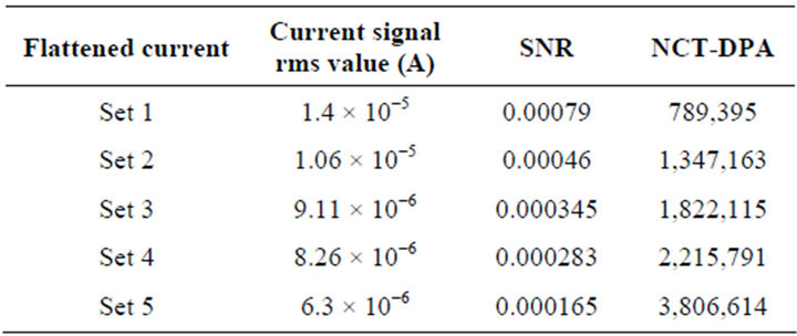
Table 5. NCT-DPA for different levels of current attenuation in the presence of the external noise.
DPA attack measurement setup. The practicality of the methodology was investigated through a case study, i.e., designing a countermeasure for which DPA can not be successful with less than 10,000 current traces. In this process, the validity of the proposed formula was also investigated by comparing NCT-DPA values obtained by the formula with those obtained experimentally.
Additionally, the SNR of DPA attacks was formulated in a new format and the relationship between NCT-DPA and the level of current attenuation was investigated in the presence of external noise. Furthermore the validity of the NCT-DPA obtained by the formula was confirmed by the rule suggested by Mangard et al. Using our formula and obtaining the linear relationship between NCTDPA and the inverse of SNR allowed us to define the efficiency gain of the countermeasure. It was shown that this parameter can be used to estimate the NCT-DPA for the flattened currents with higher levels of attenuations, where the NCT-DPA cannot be obtained experimentally.
In summary, the proposed formula is useful in two stages: 1) In the design stage, the designer can estimate the required level of attenuation for a predefined level of robustness; 2) in the simulation stage, where the situation is ideal and there is no external noise, the formula predicts the efficiency of a countermeasure in the presence of the external noise.
REFERENCES
- P. Kocher, J. Jaffe and B. Jun, “Differential Power Analysis,” LNCS Proceedings of International Cryptology Conference, Vol. 1666, 1999, pp. 388-397.
- K. Tiri and I. Verbauwhede, “Dynamic and Differential CMOS Logic with Signal-Independent Power Consumption to Withstand Differential Power Analysis,” US Patent No. 7692449, 2010.
- S. Rammohan, V. Sundaresan and R. Vemuri, “Reduced Complementary Dynamic and Differential Logic: A CMOS Logic Style for DPA-Resistant Secure IC Design,” Proceedings of International Conference on VLSI Design, Hyderabad, 4-8 January 2008, pp. 699-705.
- S. Guilley, L. Sauvage, F. Flament, V. Vong, P. Hoogvorst and R. Pacalet, “Evaluation of Power Constant Dual-Rail Logics Countermeasures against DPA with Design Time Security Metrics,” IEEE Transactions on Computers, Vol. 59, No. 9, 2010, pp. 1250-1263. doi:10.1109/TC.2010.104
- H. Vahedi, S. Gregori and R. Muresan, “On-Chip PowerEfficient Current Flattening Circuit,” Journal of Circuits, Systems, and Computers, Vol. 18, No. 3, 2009, pp. 565-579. doi:10.1142/S0218126609005332
- S. K. Kim, “Smart Cards Having Protection Circuits Therein That Inhibit Power Analysis Attacks and Methods of Operating Same,” US Patent Application, 2004/ 0158728, 2004.
- G. B. Ratanpal, R. D. Williams and T. N. Blalock, “An On-Chip Signal Suppression Countermeasure to Power Analysis Attacks,” IEEE Transactions on Dependable and Secure Computing, Vol. 1, No. 3, 2004, pp. 179-189. doi:10.1109/TDSC.2004.25
- T. S. Messerges, “Power Analysis Attacks and Countermeasures for Cryptographic Algorithms,” University of Illinois, Chicago, 2000.
- S. Mangard, E. Oswald and T. Popp, “Power Analysis Attacks: Revealing the Secrets of Smart Cards,” Springer Science, 2007.
- R. Muresan and S. Gregori, “Protection Circuit against Differential Power Analysis Attacks for Smart Cards,” IEEE Transactions on Computers, Vol. 57, No. 11, 2008, pp. 1540-1549. doi:10.1109/TC.2008.107
- ATMEL Corporation, ATmega16 Data Sheet. http://www.atmel.com/dyn/resources/prod_documents/2466S.pdf
- H. Vahedi, S. Gregori and R. Muresan, “The Effectiveness of a Current Flattening Circuit as Countermeasure against DPA Attacks,” Microelectronics Journal, Vol. 42, No. 1, 2011, pp. 180-187. doi:10.1016/j.mejo.2010.08.011