Circuits and Systems
Vol. 3 No. 4 (2012) , Article ID: 23638 , 8 pages DOI:10.4236/cs.2012.34042
Challenges in Quality Certification of I/O Libraries
Freescale Semiconductor, Moscow, Russia
Email: *osemenov@freescale.com
Received May 28, 2012; revised July 9, 2012; accepted July 16, 2012
Keywords: I/O Library; Electrostatic Discharge; Quality Certification; Latch-Up; I/O Driver
ABSTRACT
Cooperation between manufacturing and other functional groups is critical to improve the success of new products. However, integrating operations and development methodologies is often challenging due to conflicting priorities and organizational structures. Improving the quality of product development and the transition to manufacturing is not a new venture. Organizations have been incorporating planning and continuous improvement to their product development initiatives for decades. This paper summarizes the experience of I/O libraries quality certification within Freescale Semiconductor and describes the certification flow developed by Corporate Quality and I/O Design teams.
1. Introduction
The increased power consumption and higher clock frequency compromise ICs reliability and quality. More than ever, Quality has become a primary differentiator in the semiconductor industry, especially in the automotive and high performance microprocessor markets. It is important that each and every one of us understand the challenges and how to contribute to our Quality objectives.
Freescale’s goal of world-class quality demands that New Product Introductions (NPIs) are launched successfully in a robust and consistent manner. For each technology, the successful NPI requires that all elements of the technology to be brought up in a concerted manner. The Technology Certification Process (M0 (Maturity Level #0) → M1 (Maturity Level #1) → M2 (Maturity Level #2) → M3 (Maturity Level #3)) offers a method to establish interdependency of the constituent technologies and build in quality up front, thereby promoting risk-free NPI. The requirements for each constituent technology element must be met and maturity levels are granted through the review of detailed checklists generated after the silicon validation of IPs (Intellectual Property).
This paper is focused on the I/O libraries silicon validation steps that are required by the Technology Certification Process for M1, M2 and M3 maturity levels. The list of parameters of I/O cells that should be verified in silicon is common for all technologies. The provided examples are specified for cmos45soi (c45soi) I/O cells used in many Freescale products. The developed test structures are intended to measure the key parameters of I/O cells:
• Leakage current of IO cell.
• DC parameters.
• AC parameters.
• Latch-up testing (not used for SOI technologies).
• Qualification of ESD (electrostatic) protection for Human Body Model (HBM), Machine Model (MM) and Charge Device Model (CDM).
The paper is organized as follows: Section 2 presents an overview of Quality and Validation definitions. The description of concept of Technology Certification process and its major components are given in Section 3. In Section 4, the I/O test structures and measurement techniques are discussed. Section 5 deals with the resources allocation for measurements and cooperation with the test and silicon validation teams. Finally, the successful implementation of quality qualification flow and certification process for c45soi I/O libraries developed for Freescale products are presented in Section 6.
2. Quality and Validation Definitions
As the complexity of the design increases and the required time to market decreases, the need to integrate manufacturing with design becomes even more important. Integration and collaboration among development groups is suggested as one factor that improves the success of new products. Generally, a customer regards a product to be of high quality if the product is meeting their requirements at lowest possible cost. Quality can be expressed as the number of customer returns per million or Parts Per Million (PPM):

Or, in another view, quality is related to the population of faulty devices that escape detection at the supplier’s plant. The simplest Quality definition that frequently cited by Program Management is “Quality is consistently delivering products that meet customer requirements”. Verification, validation and certification are needed to confirm “meeting customer requirements”. Repeatable processes ensure “consistent” quality. Appropriate communication in the form of user documentation, training and application support, assist the supplier to deliver their products with a high quality.
When I/O team is tasked with development and delivery of a product, it needs to know how the product will be used and the success criteria before the defining what to develop. Prerequisites of successful development of any I/O library include a good requirements gathering, documentation and verification practices that address how to verify the product quality. I/O teams should put a strong emphasis on validation of all deliverables, both as standalone entities and in conjunction with other IP deliverables. The close cooperation with Corporate Quality team is absolutely needed.
3. Technology Certification Process for I/O Libraries
The term “Technology Certification” as used here includes all major elements required to execute an NPI I/Os, and goes well beyond the traditionally emphasized die processing and packaging aspects. The Technology Certification process determines the maturity/readiness of I/O library according to four maturity levels (M0, M1, M2, & M3), which are awarded after achieving the milestones consistent with the NPI flow from Planning, Prototype, Pilot and Production stages, respectively. These 4 levels (level 0 - 3) reflect the key milestones of readiness from “Technology Specification Defined” through “Ready for Product”. The requirements for the entire platform must be satisfied in order to achieve a given certification level for I/O library. Maturity levels are granted through the detailed checklists of intermediate deliverables that are reviewed across all functional areas. The typical checklists for I/O libraries are given below.
1) Maturity Level 0—Specification Defined
• Level 0 PDK (Process Development Kit) is available with required components for IP design and implementation.
• Statement of Work (SOW) is complete and under revision control. SOW signed by stakeholders.
• Silicon validation plan is in place.
• All flows and methods have been identified and are aligned with PDK supported tools list.
• Product groups define initial ESD requirements for products including I/O operating specs, voltage ranges, device configurations to be protected, ESD stresses required for qualification, and any special application requirements.
2) Maturity Level 1—Ready for Design
• PDK release has passed level 1 Milestone specification.
• I/O library design review sign-off (conformity to SOW specification).
• Front End (FE) and Back End (BE) view validation tests have been implemented in IP environment.
• I/O IP available for test vehicles (TV).
• ESD parameters are characterized based on test vehicles and results are available.
• DFM (Design for Manufacturing rules) score requirements are verified.
3) Maturity Level 2—Ready for Prototype
• PDK used for IP development reached M2.
• Actual silicon available for M2 validation with all critical parameters in the following range: typical ± 3 sigma.
• M2 Silicon Validation report completed (Test and Characterization report).
• For all I/O library specifications, actual results within CAD data for WCS (Worst-Case process corner) to BCS (Best-Case process corner) envelop.
• ESD validation report from TV complete and released by the ESD team, product group, and Quality organization (including F/A (Failure Analysis) results for failures).
4) Maturity Level 3—Ready for Product
• PDK used for IP development reached M3.
• Actual silicon available for M3 silicon validation with all critical parameters in the following range: targeted process corner ±3 sigma.
• ESD testing and qualification results available from NPI silicon and corrective actions identified on key issues.
• M3 Silicon Validation report completed.
Finally, the Technology Certification Process has a direct impact on reducing defects at customer site, customer quality incidents (CQI) return rate, reduce average CQI cycle time and reduce customer reported PPM.
4. I/O Test Structures and Measurement Techniques
The list of parameters of IO cells that should be verified in silicon is common for all technologies. However, the provided examples in this paper are mostly specified for c45soi IO cells. Test structures are intended to measure the following key parameters of IO cells library:
• Leakage current of IO cell.
• DC parameters.
• AC parameter.
• Latch-up testing (not used for SOI (Silicon-on-Insulator) technologies).
• Qualification of ESD protection for HBM, MM and CDM ESD stresses.
Figure 1 presents the test structures for c45soi LVCMOS I/O library validation, as an example. Similar test structures can be developed for other technologies based on the ESD Integration Guidelines/Rules specified by ESD team. It includes the following functional blocks:
1) The worst case of I/O segment (Pad1 - Pad5) with respect to ESD stress as shown in Figure 1, Segment 1. This I/O segment has a minimal number of distributed ESD clamps needed to discharge the required ESD current following the ESD integration rules.
2) I/O cell banks for leakage current measurements: (Pad1 - Pad5) and (Pad6 - Pad14) as shown in Figure 1 of Segment 1 and Segment 2, respectively.
In Figure 1, “Term”, “Clamp” and “Trigger” mean the Termination cell, I/O cell with ESD clamp and I/O cell with ESD trigger, respectively.
4.1. ESD testing
ESD protection should be typically sufficient for:
• Human Body Model (HBM)—2 kV.
• Machine Model (MM)—200 V.
• Charge Device Model (CDM)—500 V.
HBM/MM testing is performed in accordance with the ESD association specification:
• Each I/O pin should be stressed against each power supply pin and GND pin.
• Each power supply should be stressed with respect to other power supplies.
• Three repeated ESD zaps in sequence in ESD tester are required, and there should be at least a 300 ms interval between consecutive zaps. It is recommended to run the set of HBM zapping first and then run the set of MM zapping.
The worst case of I/O segment (Pad1 - Pad5) with respect to ESD stress is shown in Figure 1 (Segment 1).
Item #1 The ESD spec that should be used for ESD testing is the JEDEC standard [1-3].
Item #2 The ESD failure is determined as a significant difference in leakage current between before and after ESD stress on OVDD & IVDD power domains or input leakage current (Iih, Iil) on inputs of IO cells in Segment 1. The ESD failure is occurred if the leakage current difference is exceeded 1mA.
Item #3 The matrix of voltages for ESD testing that should be used is the following:
HBM: 500 V, 1000 V, 1500 V, 2000 V, 2500 V (positive and negative pulses).
CDM: 250 V, 350 V, 500 V, 550 V.
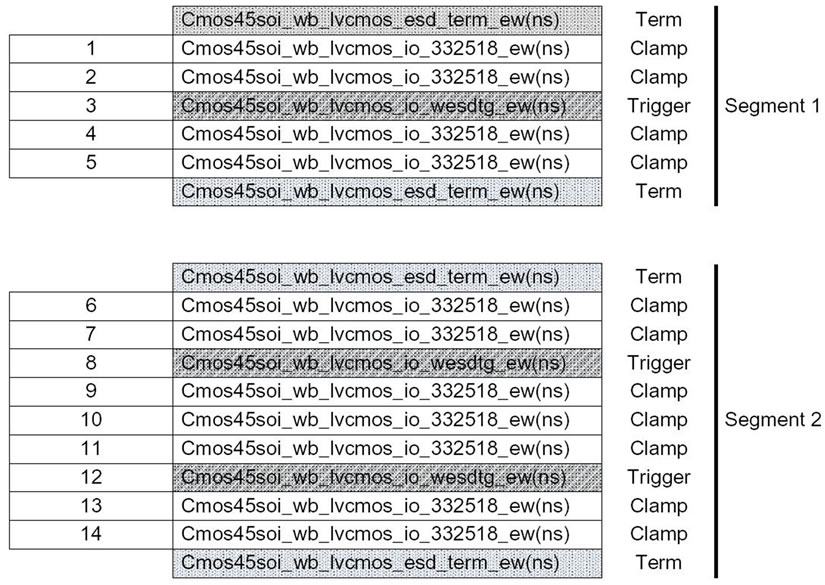
Figure 1. The test structures for c45soi LVCMOS I/O library validation.
MM: 100 V, 200 V, 250 V.
Item #4 Each of the above mentioned ESD stresses should be applied to each input pad (chip_pad) of I/O cell in I/O segments when GND pad is grounded.
For Segment #1, each of five input pins should be stressed with respect to grounded GND pad and floated OVDD & IVDD.
And, each of five input pins should be stressed with respect to grounded OVDD pad and floated GND & IVDD.
And, each of five input pins should be stressed with respect to grounded IVDD pad and floated GND & OVDD.
Three repeated ESD zaps are required for each test case.
The ESD procedure and pin grouping mentioned above is also defined in JEDEC spec. The pins that are not used in a particular ESD stress should be floated.
Note: It’s not necessary to repeat the ESD tests for Segment #2, which is used for leakage current measurements only.
Item #5 Power domain to power domain stresses within Segment 1 should be performed. It includes OVDD to VSS, IVDD to VSS and OVDD to IVDD ESD stresses.
Item #6 The segment to segment power domain ESD stressing is required. It should be OVDD of Segment 1 to OVDD of Segment 2 ESD stressing. It means that ESD stress is applied to OVDD of Segment 1 and OVDD of Segment 2 are grounded and vice versa.
4.2. Measurement of Leakage Current
Figure 1 shows the circuit that should be used for leakage current measurements of IO cell. “Term” cell is the ESD termination cell. This circuit consists on two segments. Segment 1 and Segment 2 should have separated OVDD and IVDD. All IO cells in these segments should be used in the same operating mode “input”, “output” or “tri-state”.
Measurements of leakage current are performed for OVDD and IVDD supplies.
Ileakage current (for one IO cell) = (Isegment 2 – Isegment1)/4
4.3. Measurement of DC Parameters
DC parameters include
• VOH and VOL.
• IOH and IOL.
• Tri-state input current.
Generally, DC parameters should be measured for 3 units (packaged chips) for all power supplies (OVDD ±10%) specified in Specification and three temperatures for each OVDD. The details are given in Table 1 for c45soi 49 μm pitch LVCMOS IO library or GPIO (General Purpose) IO library, as an example. Measurements should be performed for all process corners (Best, Typical, Worst) available from the Fab.
4.4. Measurement of AC Parameters
Generally, AC parameters for IO libraries are including the operating frequency or delay and Rise & Fall times.
4.4.1. Measurement of Ring Oscillator Frequency of IO Cells
The block diagram to measure the ring oscillator frequency of IO cells is shown in Figure 2. The ring oscillator includes twelve IO cells and nand2 cell. The first implementation of ring oscillator (top part) is placed inside of chip to eliminate the parasitic capacitances of wire bonding and packaging. The second implementation of ring oscillator (bottom part) is placed in the IO segment to estimate the impact of package parasitics. The signals “en_osc1” and “en_osc2” are the control signals to switch on/off the ring oscillators: ON (if en_osc<1:2> ='0') or OFF (if en_osc<1:2>='1').
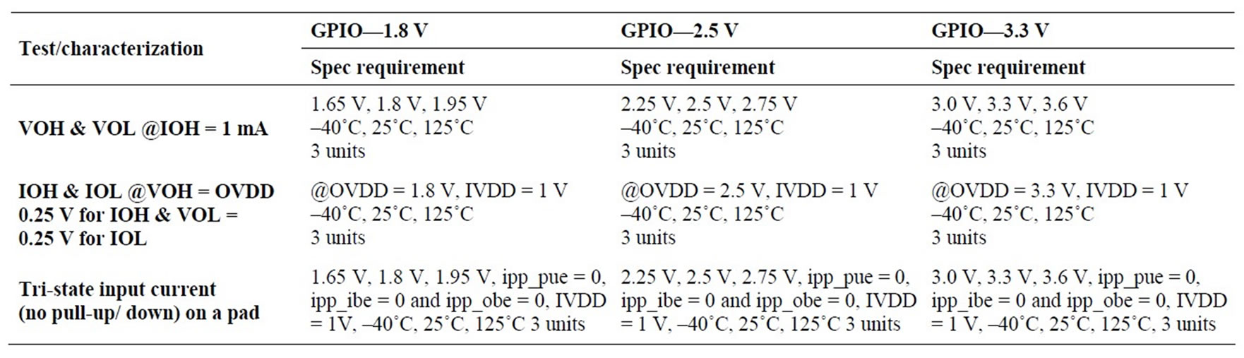
Table 1. DC parameters for c45soi LVCMOS IO library.
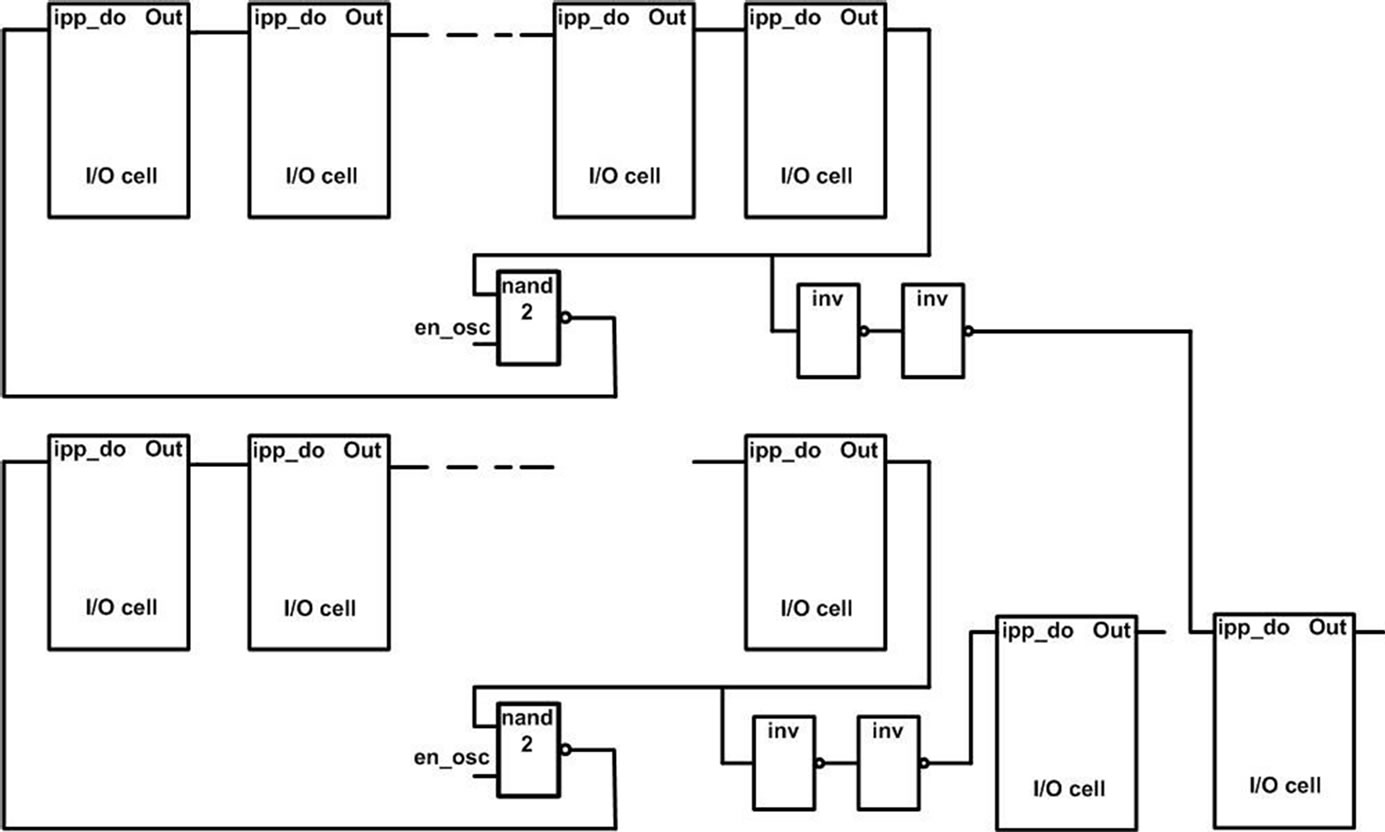
Figure 2. Block diagram to measure frequency of ring oscillator for IO cells.
4.4.2. Measurement of Rise and Fall Times of IO cell
Generally, the Rise and Fall times should be measured for all OVDD and core voltages (IVDD) given in the Specification for IO Library at three temperatures and all process corners available from Fab.
Table 2 presents the example of Rise and Fall times requirement for 49 um pitch LVCMOS IO library. Rise and Fall time measurements should be performed at each OVDD & IVDD = 1 V for three temperatures 125˚C, 25˚C and –40˚C.
4.5. Latch-Up Testing for IOs
Latch-up testing should be performed for IO cells implemented in bulk technologies. Latch-up testing is not required for IO libraries fabricated in SOI technologies.
Latch-up testing of IO cells should include the I-test and Over-voltage latch-up tests for Class I (Level A) performed at room temperature. Note: Class II (high temperature latch-up tests) can be required for some special applications as well.
I-test: A latch-up test that supplies positive and negative current pulses to the pin under test.
Over-voltage test: A latch-up test that supplies overvoltage pulses to the Vsupply pin under test.
4.5.1. I-Test
For I-test, the trigger current should be ±100 mA applied for all pins for product level testing. In case of latch-up testing for Test Vehicle (TV), the IO pins should be grouped by functionality and at least one pin from each group should be tested. IO pins should be tested in all possible operating states or the worst case operating state. IO pins should be tested in the high impedance state or in the valid logic state. After latch-up testing, all devices must pass the functional testing. The equivalent circuits for positive and negative I-test latch-up testing are shown in Figures 3 and 4, respectively.
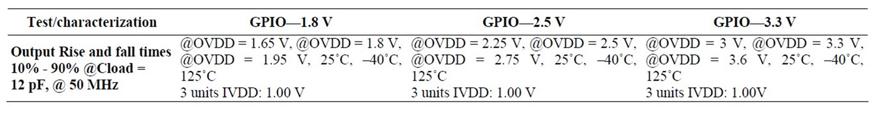
Table 2. Rise and fall times measurement requirements for 49 μm LVCMOS IO library.
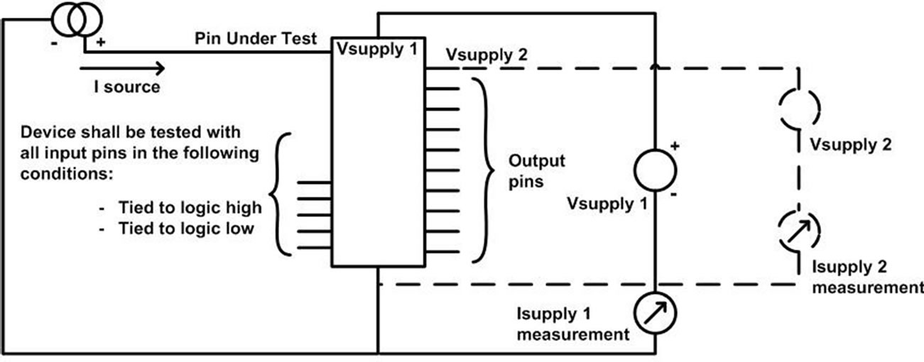
Figure 3. The equivalent circuit for positive I-test latch-up testing [4].
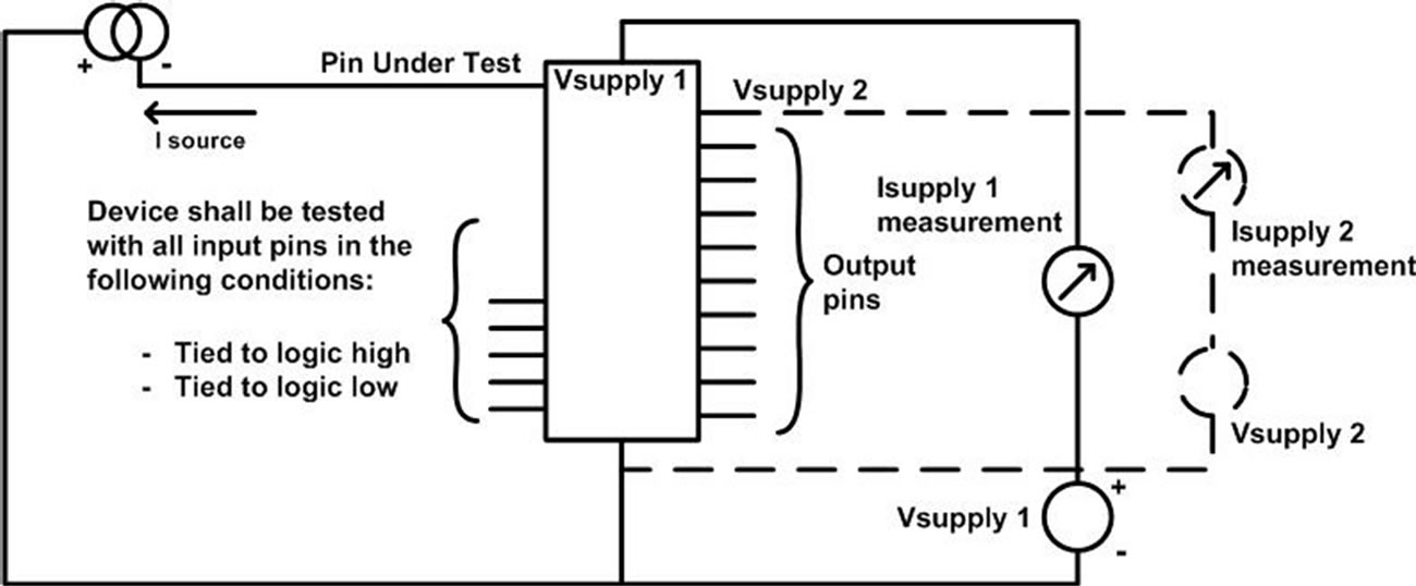
Figure 4. The equivalent circuit for negative I-test latch-up testing [4].
4.5.2. Over-Voltage Latch-Up Test
The Vsupply over-voltage test should be performed on each Vsupply pin or pin group. To provide a true indication of latch-up for the given test conditions, the input pins are configured as logic-high states. They should remain within the valid logic-high region as defined in the device specification. In case of over-voltage latch-up testing, the voltage trigger source equaled to 1.5 × Vsupply max should be applied for each Vsupply pin. In case of over-voltage latch-up testing for Test Vehicle (TV), the Vsupply pins should be grouped by voltage nominal and at least one pin from each group should be tested. The equivalent circuit for over-voltage latch-up testing is given in Figure 5. After the trigger source has been removed, return the Vsupply pin under test to the state it was in before the application of the trigger pulse and measure the Isupply for each Vsupply pin (or pin group). If any Isupply is greater than or equal to the failure criteria, the latch-up has occurred and power must be removed from the DUT. The failure criteria is the absolute Isupply after test >1.4 × Inom before test.
5. Execution of Validation Flow— Stakeholders and Communication
The process of the library development has to be aligned with the NPI process. The Quality audit checklist requires validation resource allocation at the very early development phase (Planning). During Planning period, the SoW (Statement of Work) has to be created and approved by customer, including scope, schedule, and resources. Resources allocation can be done using RAFT or Primavera tools. Technical specification has to be created, however, at this phase it does not have to be finalized yet. At the end of this phase, the IP validation plan is required. It should include the list of library views and pre-silicon simulation results. In addition, the Initial Silicon validation plan has to be created. It consists of two parts defining What has to be measured, Who has to measure it and When, the list of critical parameters of I/O cells taken from specification, and resource allocation approved by stakeholders. Usually, at this early phase the NPI roadmap is not finalized yet and the First silicon and NPI certification dates will be determined at the next library validation phase. Each level of Maturity audit assumes Technology, Models, and PDK to be at the same Maturity level, so all collateral plans are mutually dependent. Every one audit must close all the risks identified by the previous audit.
Prototype, followed by the Pilot, is a part of Execution phase. The gate between Prototype and Pilot is M1 audit and the approval of PSC meeting. When the I/O library development process is completed, the final library is delivered to customer during the Prototype phase. At the time of M1 audit, the silicon data may be or may not be available for the given IP, so the quality assessment of the IP can be done based on simulations and view validation process, which include DRC/LVS checking, unit testing, simple integration tests and other tests. Before M1 audit, the silicon validation plan has to be finalized, approved and committed by the Test engineering team.
For I/O libraries, the Silicon Validation plan usually contains sections for DC, AC and ESD data. If NPI follows the complete lifecycle process, all three groups of parameters can be measured both on Test Vehicle (TV) and product. The TV usage is a good opportunity to get early silicon data with a complete set of measurement structures at different process corners. As opposed to the TV, the measurement of I/O data on product has a limited capability. For example, the packaged products do not allow to measure I/O buffer delay. As a workaround, SGPC ring oscillator can be used for this kind of measurements. Unfortunately, frequently the development program skips the TV phase for some reason, for example limited budget. Usually, DC data measurements are performed using the Automated Test Equipment (ATE). AC data are measured on Lab test bench. ESD tests require special equipment. Hence, different Test engineering teams are involved in the measurement process. The getting validation data on time requires certain communication and coordination efforts from all stakeholders.
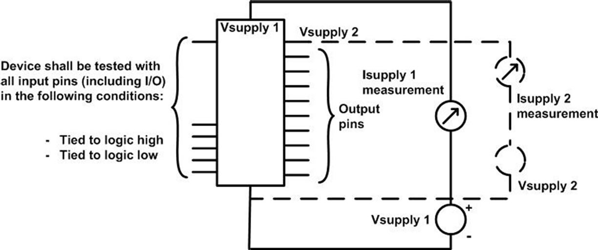
Figure 5. The equivalent circuit for Vsupply over-voltage latch-up testing, adopted from [4].
M2 audit is a gate from Pilot to Certification phase. For M2 audit, silicon validation data have to be available. The respective checklist requires to have the measurement results within ±10% of typical simulation results. To get a good match, the test environment parameters have to be carefully estimated, such as a load capacitance, tester or oscilloscope parasitics, package and transmission line parameters.
M3 audit completes the Certification step and leads to the Production phase. M3 silicon validation deals with the IP performance, functionality and reliability over the process window, so the matrix lot measured data are needed.
There are certain potential difficulties with the practical implementation of described above scheme. 1) They come from the fact that IP is permanently improving during the development process. Every drawback found from any source (simulation data, test vehicle development, or the sample product) is being followed up with IP changes. As a result, the IP versions used on different certification phases are different. The changes in IP have to be tracked down, and their impact on the quality has to be understood and estimated; 2) I/O library re-usage in new products provides more opportunities to get silicon validation data, so the I/O IP may need to be re-validated on every new product.
6. Conclusion
The emphasis of product quality planning is the way to prevent the development and manufacturing problems. There is no way to plan for every possible issue that may happen with a complicated new product development process of semiconductor devices. Maturity qualification flow of semiconductor IPs is not simply a quality planning tool, more importantly it is a philosophy that must be integrated throughout the organization. The maturity qualification methodology described in this paper was successfully applied for different bulk and SOI I/O libraries used in many Freescale products. The silicon validation and quality verification of I/O IPs at early development stages allow us to cut the product costs, to improve the time to market for Freescale products and to reduce the number of engineering re-designs.
REFERENCES
- JEDEC CDM, 2012. http://www.jedec.org/sites/default/files/docs/22C101E.pdf
- JEDEC HBM, 2012. http://www.jedec.org/sites/default/files/docs/js001-2011.pdf
- JEDEC MM, 2012. http://www.jedec.org/sites/default/files/docs/22A115C_0.pdf
- JEDEC Latch-Up, 2012. http://www.jedec.org/sites/default/files/docs/JESD78D.pdf
NOTES
*Corresponding author.