Circuits and Systems
Vol. 3 No. 3 (2012) , Article ID: 20199 , 6 pages DOI:10.4236/cs.2012.33029
Design and Implementation of an Analogue Tester Board*
Electrical Engineering Department, Engineering College, University of Anbar, Al-Anbar, Iraq
Email: yousif_phd@hotmail.com
Received February 16, 2012; revised March 21, 2012; accepted March 28, 2012
Keywords: Tester Board; Electronic Components; Electronic Diagnostic Systems
ABSTRACT
The recent rapid development of electronics and continual increase of the complexity and variety of electronic circuits (chips, packets, microand embedded systems) creates a demand for viable test and diagnostic methods. These recent developments have led to a great deal of research interest in electronic diagnostic systems, especially of effective diagnosis methods of detection, localization and identification levels of hard (catastrophic) and soft (parametric) faults in analog circuits. At present, the majority of electronic devices (embedded systems) are designed based on digital circuits; however a lot of them also contain analog components that require more complicated testing techniques. This paper presents a novel, electronic components tester board with inside, outside of circuit under tested. The design is first simulated by using the electronic work-bench software Multisim 11 in order to obtain satisfactory theoretical results for each standalone element of the design. Thereafter, the design is practically implemented and experimentally verified to show agreement with the simulated results.
1. Introduction
The different type of electronic equipment that has invaded our offices and homes these days is mind boggling. Numerous appliances we use at home and office are remote-controlled, for example, television (TV), air-conditioners, audio equipment, telephone, etc. It almost seems like magic how even a child, can switch channels, or increase and decrease the volume on a TV set at home by just clicking on a few buttons sitting at the comfort of a sofa away from the television apparently without any physical wiring or connection [1]!
Again, it is astonishing how easy it is to communicate with people living several thousands of kilometers away, from any place at home, office, on the road in a car, or in a classroom by just clicking a few numbers on palm sized cellular phones. One of the most important concerns related with electrical and electronic gadgets and equipment is their power consumption. Nowadays, consumers would like to know the specifics of every electrical and electronic item before buying a product for residential or commercial purposes. So, commercial electrical and electronic devices must match international quality standards in terms of operation, efficiency and functionality to be able checking with standard [2,3].
For construction of the tester board discussed in this paper, it was a requirement that all the components should be able to be mounted on a small PC. There are a number of different suitable cases and even a small one will fit the board. Despite initial reluctance to use a soft casing for fears that it would not be suitable, subsequent testing proved that it was the best choice for the board the soft plastic is more durable and will not fracture if dropped or bumped. Rigid styrene cases tend to crack very easily and during development, one styrene case was crushed under foot when it fell on the floor [4].
The case is the first item to be purchased as it dictates the maximum height for the components. If some of the parts are too high, they can be bent over during assembly and it’s important to know this before designing the remaining of the board. Next, the slide switch needs to be selected for the right size of the board. The switch supplied in the kit fits exactly into the holes and any mounting flanges must be cut off so that the board will slide neatly into the case. It should be noted during soldering of the switch that a long soldering job may cause flux leakage along the switch leads causing contact faults. Assembly should be started at one end of the board and each component fitted in sequence. The LED, transistors, diodes and electrolytic must be fitted around the correct way following the layout on the board. Finally, the probe tip is made from a small nail and soldered to the underside of the board. The two cells are soldered to the board with short lengths of tin [5,6].
The various types of electrical and electronic tester boards are classified according to the electronic components being tested. Any electronic component may be classified as passive or active. The formal physics definition treats passive components as ones that cannot supply energy themselves; whereas a battery would be seen as an active component since it truly acts as a source of energy. However, electronic engineers performing circuit analysis use a more restrictive definition of component power consumption. When the concern is with the energy due to signals it is convenient to ignore the DC circuit and pretend that the power supplying components such as transistors or integrated circuits are absent (as if each such component had its own battery built in), although it may in reality be supplied by the DC circuit which is being ignored. Then, the analysis only concerns the so, called AC circuit; an abstraction which ignores the DC voltages and currents (and the power associated with them) present in the actual circuit. This technique, for instance, allows the modeling of an oscillator as “producing energy” even though in reality the oscillator consumes even more energy from a power supply, obtained through the DC circuit which has been ignored. Under such restrictions the following terms used in circuit analysis can be defined as follows [7-9]:
• Passive components are ones which cannot introduce net energy into the circuit they are connected to. They also cannot rely on a source of power except for what is available from the (AC) circuit they are connected to. Consequently, they are unable to amplify (increase the power of a signal), although they may well increase a voltage or current such as is done by a transformer or resonant circuit. Among passive components are familiar two-terminal components such as resistors, capacitors, inductors, and most sorts of diodes.
• Active components rely on a source of energy (usually from the ignored DC circuit) and are usually able to inject power into a circuit. This includes amplifying components such as transistors, triode vacuum tubes (valves), and tunnel diodes. Passive components can be further divided into lossless and lossy components [10-12].
• Lossless components do not have a net power flow into or out of the component. This would include ideal capacitors, inductors, transformers, and the (theoretical) gyrator.
• Lossy or dissipative components do not have that property and generally absorb power from the external circuit over time. The prototypical example is the resistor. In practice all non-ideal passive components are at least a little lossy, but these are typically modeled in circuit analysis as consisting of an ideal lossless component with an attached resistor to account for the loss.
Most passive components with more than two terminals can be described in terms of two-port parameters satisfying the principle of reciprocity. In contrast, active components generally lack the property of reciprocity. Such distinctions only apply to components modeled as elements within circuit analysis. Practical items, which act as transducers or have other connections to the outside world such as switches, cannot be subject to this form of classification since they defy the view of the electronic circuit as a closed system. This work consists of introduction, design of model of tester board, the hardware design of board, results and discussion of results and conclusions.
2. Design the Model of Tester Board
The design and implementation of the developed model has two phases. The first presents the theoretical design by software which consists of simulating the circuit to verify the correctness of the design and the second step presents the practical implementation and testing of the model with different components. Both these steps are explained in detail in the following sub-sections.
2.1. Simulation
The theoretical design of the electronic tester and its simulation is achieved by using the electronic workbench software MultiSim Ver. 11.0.1. Initially, the circuit was designed in order to test the operation of each component in a standalone fashion. Two types of checks are implemented for components: in context of the electric circuit and outside of the circuit (without any connection). Some of these circuits are shown in Figures 1 and 2. Thereafter, these circuits are reduced to a single circuit (as shown in Figure 3) that is used for the purpose of testing within the context of the circuit. The procedure of checking the electronic components can be carried out with this circuit by the following steps that are related to the type of component which is taken under test. An example that will be considered is that of a MOSFET. The operation of a MOSFET (N-channel and P-channel) when it is connected in the circuit or individually can be checked by the following procedure:
• Connect the transistor with the tester board with the source at position (a), gate at position (c) and drain at position (b).
• Connect plugs to J5 and J4 for N-channel MOSFET, or J2 for P-channel MOSFET.
• Press the push switch and check the two LED’s. For an operative N-channel transistor, LED2 will flash repeatedly; and for an operative P-channel transistor, LED1 will flash repeatedly. If the opposite LED’s flash, then the transistors are inoperative. If both LED’s flash, then the transistor is in open circuit; and if both LED’s are off, the transistor is in short-circuiting.
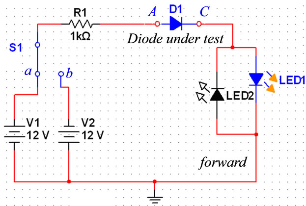

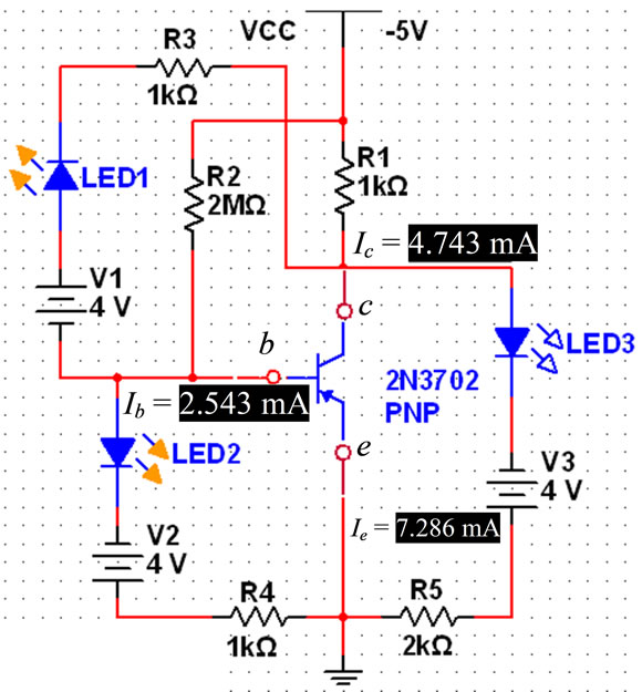

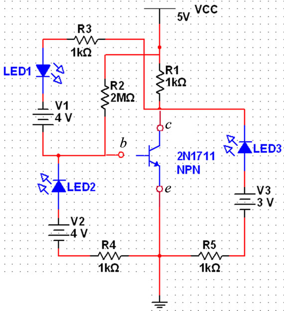
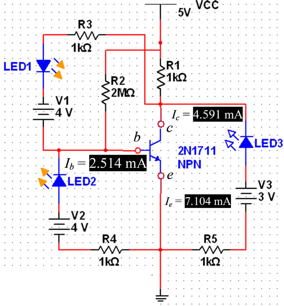
Figure 1. The first part of circuits for checking the electronic components individually form.
A summary of the procedure for checking all analogue electronic components in the circuit shown in Figure 2 as well as the various expected outputs and their indication is given in Table 1.
2.2. The Hardware Design
After the simulation results proved the circuit in Figure 3 could be used as a general design and the input-output configuration and connection procedure was derived for us in Table 1, it only remained to implement the circuit design in a practical way. The circuit was implemented with suitable biasing configuration and two options of power supply (an internal 9 V battery or any external power supply). Images of the practical model are shown in Figure 4.
The procedure for connection and testing with the practical model are similar to the procedure as explained in the simulation setup. For example when we need check any component such as P-ch JFET (Junction field effect transistor) for operation can be done by the following procedure:
• Set the board that is shown in Figure 4 for any select of power supply (external power supply or internal).
• Made the connection of JEFT piece according to connect table shown in Table 1. The point connection


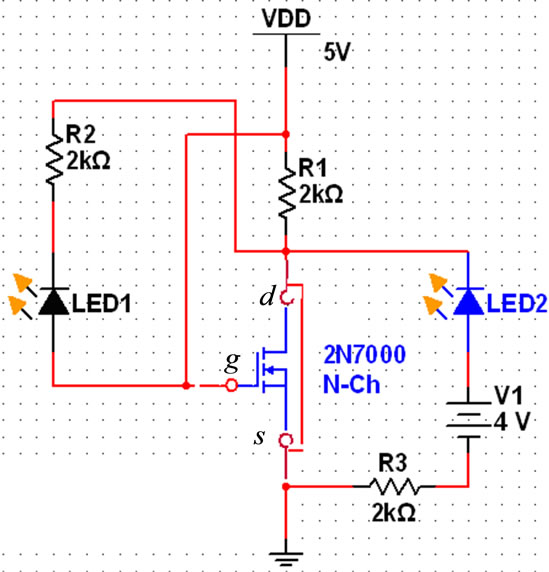
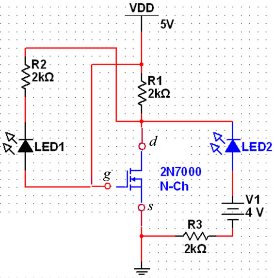

Figure 2. The second part of circuits for checking the electronic components individually form.
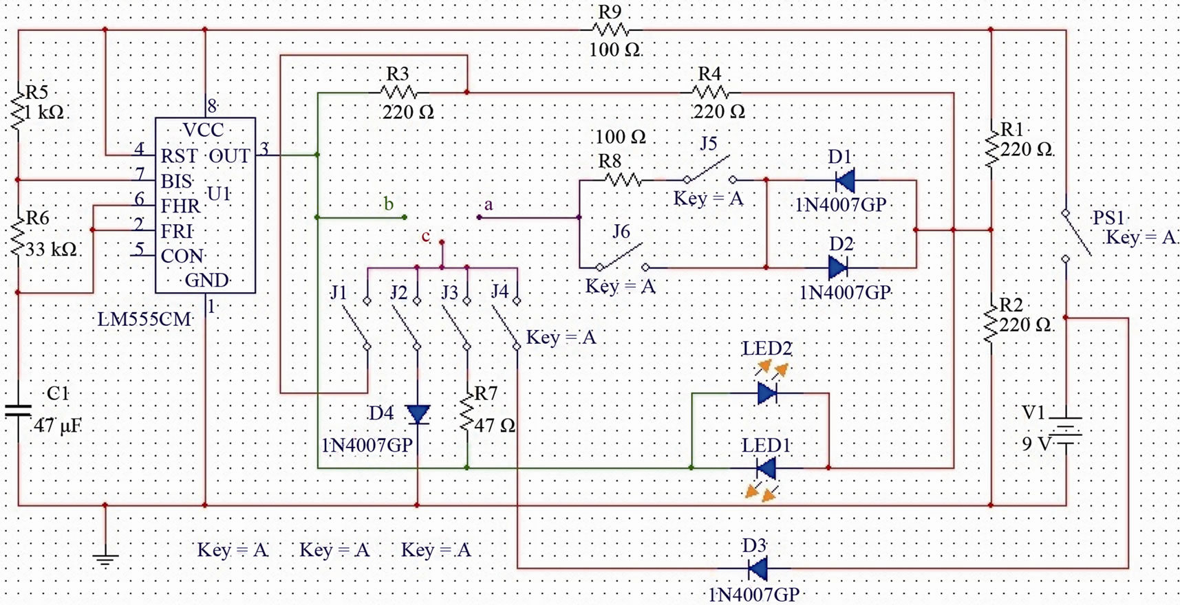
Figure 3. Simulation of model by software (Multisim 11.0).
is J3 and J6 to connect the terminals of JEFT at the points A, B and C according to Table 1 and Figure 4.
• Check your connection then, press the push button S1 to get the results (see Figure 4). According to Table 1. When the JEFT is operating the LED1 is flash otherwise no response indicates to the JEFT is short cct
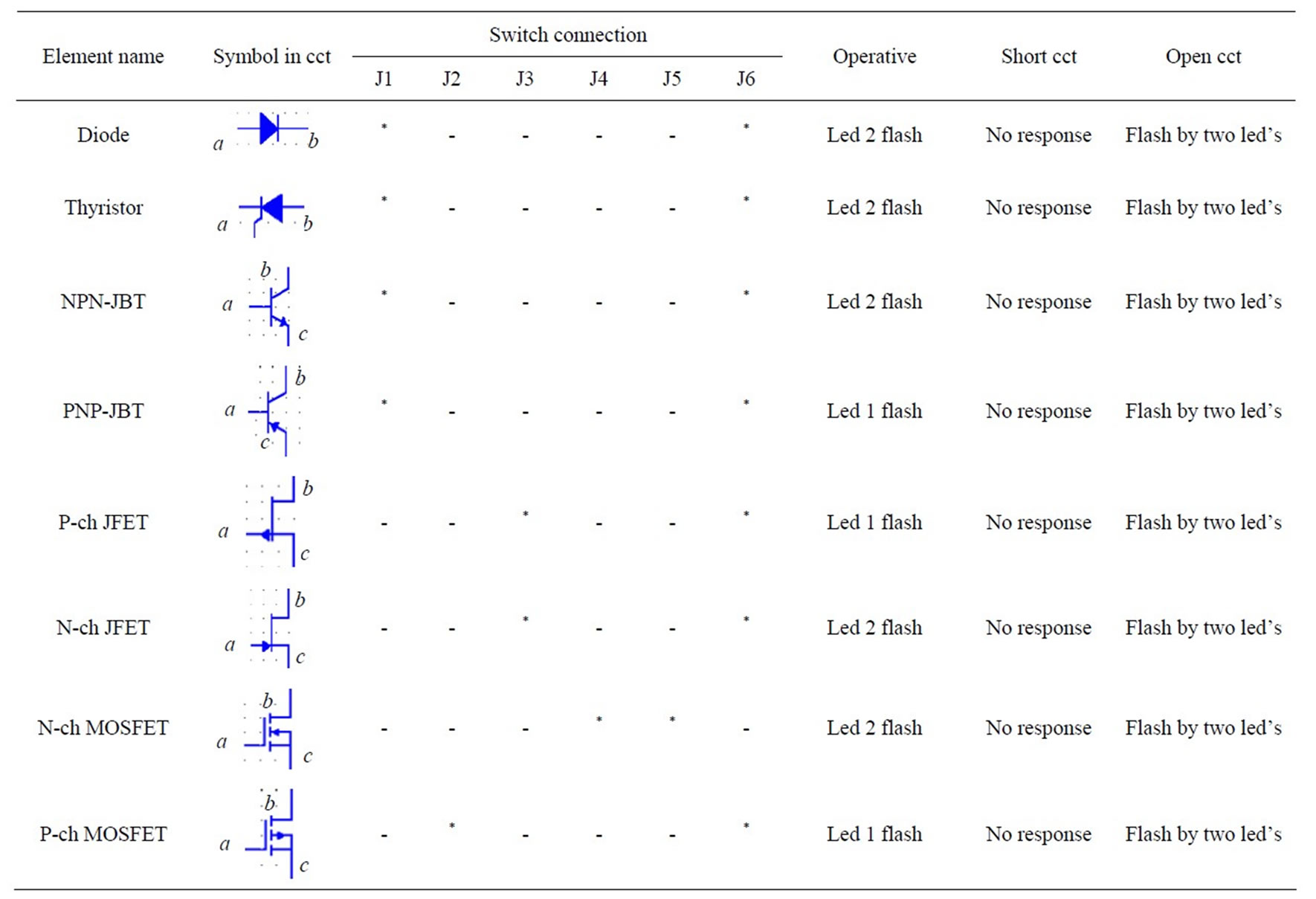
Table 1. The connection of components and testing decision (* ≡ Switch ON).
(damage) and flash by two LDE’s is open cct.
The general procedure for using this trainer by checking the operation of any electronic piece by theoretical study after that made the procedure which shown above to take the suitable discussion about the piece under test.
3. Results and Discussion
Depending on the individual operation principles of the electronic components, the tester board was designed for checking the components outside of the circuit. However, as increased faults happen during the operation of the electronic components, this necessitated the requirement to design a tester to perform within a circuit that used the component under test. The first design that tested electronic components within a circuit was limited to diode and BJT. Since an electric circuit has many types of these components like ssSCR, MOSFET and JFET’s, the general tester model was designed. After the initial design of Figures 1 and 2, was used in testing it became clear that it needed R9 (100 ohm) to limit the current which passes through the 555IC when the electronic device under test is shorted.
In addition, for MOSFET testing, it also became clear that if the MOSFET is shorted, the circuit would be shorted at the source. This prompted the use of a diode on the gate to prevent the source from being shorted. This design offers a very important facility for any designer in electronic circuits where by using the model for testing transistors it has ability to estimate the type of the transistor with the output configuration as follows:
• If only LED2 flashes, the type of the transistor is NPN for a BJT and P-channel for a JFET.
• If only LED1 flashes, the type of the transistor is PNP for a BJT and N-channel for a JFET.
To more explain the procedure of checking the types of transistor and its operation. The following example will discuss the Bipolar Junction Transistor (BJT) by the following steps:
• Connect the transistor in tester board where collector in position (a), base in position (c) and emitter in position (b), as shown in Figure 4.
• Connect the J1 and J6.
• Press bush switch, then check the two LED’s. For NPN transistor if only LED2 will flash intermittently, this means that the transistor is operative, otherwise, it is in operative.
• If the transistor is PNP only LED1 will flash inter-

Figure 4. The practical model of electronic tester board.
mittently, this means that the transistor is operative.
• Otherwise, it is in operative. If the transistors are open-circuit the two LED’s will flashes intermittently. If the transistors are short-circuiting the two LED’s won’t flash.
4. Conclusions
This paper presents a design for an electronic tester board and provides details of its development. From the simulation results and the practical implementation and experimentation of the board with many components it can be seen that the circuit implemented in the tester model offers several electronic component testing abilities as follows:
• It has the ability to check the electronic components as listed in Table 1 independent of the external circuit.
• It has the ability to check the elements within the context of the electric circuit without removing the element from circuit. This option easily facilitates repairing of electrical boards by minimizing the cost and time for the designer.
• In transistor applications the board has the ability to determine the specific type of transistor being used and classify it in the appropriate category of (ssSCR, MOSFET, JFET) transistor.
Finally, an additional advantage is that this design is small and light enough to be used in portable form, or also in the laboratory where it offers two power supply options.
REFERENCES
- Z. Czaja, “Testing of Analog Parts of Electronic Embedded Systems with Limited Access to Internal Nodes,” 12th IMEKO TC1 & TC7 Joint Symposium on Man Science & Measurement, Annecy, 3-5 September 2008, pp. 305-312.
- I. Memis, “Testing to Eliminate Reliability Defects from Electronic Packages,” 43rd Annual Proceedings of Reliability Physics Symposium, 17-21 April 2005, pp. 462- 465.
- B. Betts, “Diagnosing and Fixing Motherboard Faults,” 1997. http://people.richland.edu/dkirby/mbdfaults.pdf
- Company Manual, “Front Panel I/O Connectivity Design Guide,” Intel Corporation, Copyright 2000, Order Number A29286-001.
- L. Wang and M. S. Abadir, “On Efficiency Producing Quality Tests for Custom Circuits in Power PCTM Microprocessors,” Journal of Electronic Testing: Theory and Applications, Vol. 16, No. 1-2, 1999, pp. 121-130.
- Dell South, “Basic Electronics Testing Study Guide,” USA an Equal Opportunity Employer, 2005.
- K. Warren, D. Roth, J. Kinnison and B. Carkuff, “Single Event Latchup and Total Dose Testing of Spacecfat Electronic Components,” Radiation Effects Data Workshop, 2001, pp. 100-105.
- H. Livingston, “Avoiding Counterfeit Electronic Components—Part 2 Observations from Recent Counterfeit Detection Experiences,” BAE Systems Information and Electronic Systems Integration Inc., 2007, pp. 1-4.
- J. Yong, “7 Ways on How to Save Your Time for Electronic Repairing Line,” 2011. http://www.Testingelectroniccomponents.com
- Altera DE2 Board, “Development and Education Board Getting Started Guide,” Document Version 1.2, 2005.
- Instruction Sheet, “Thermo Scientific Orion Electronic Test Kit”, 2011. http://www.thermo.com/eThermo/CMA/PDFs/Various/File_9126.pdf
- J. Yong, “How to Solve No Power Problem in HP f1723 LCD Monitor,” 2011. http://ezinearticles.com/?HP-F1723-LCD-Monitor-Repair---No-Power&id=914512
NOTES
*Design and Implement analogue electronic tester board.