Circuits and Systems
Vol. 3 No. 2 (2012) , Article ID: 18530 , 10 pages DOI:10.4236/cs.2012.32017
Analytical and Numerical Model Confrontation for Transfer Impedance Extraction in Three-Dimensional Radio Frequency Circuits
1R3 Logic Inc., Monbonnot-Saint-Martin, France
2Université de Lyon, Villeurbanne, France
3Faculty of Engineering, Ain Shams University, Cairo, Egypt
Email: Christian.Gontrand@insa-lyon.fr
Received November 9, 2011; revised December 9, 2011; accepted December 19, 2011
Keywords: Through Silicon Via (TSV); Green’s Function; Transmission Line Model; Radio Frequency (RF); Transfer Impedance Extraction
ABSTRACT
3D chip stacking is considered known to overcome conventional 2D-IC issues, using through silicon vias to ensure vertical signal transmission. From any point source, embedded or not, we calculate the impedance spread out; our ultimate goal will to study substrate noise via impedance field method. For this, our approach is twofold: a compact Green function or a Transmission Line Model over a multi-layered substrate is derived by solving Poisson’s equation analytically. The Discrete Cosine Transform (DCT) and its variations are used for rapid evaluation. Using this technique, the substrate coupling and loss in IC’s can be analyzed. We implement our algorithm in MATLAB; it permits to extract impedances between any pair of embedded contacts. Comparisons are performed using finite element methods.
1. Introduction
As the complexity of mixed digital-analog designs increases and the area of the current technologies decreases, substrate noise coupling in integrated circuits becomes a significant consideration in the design. Nowadays, nanotechnology and the development of semiconductor technology enable designers to integrate multiple systems into a single chip, not only in 2D (planar), but also in 3D (in the bulk). This design technology reduces cost, while improves performance and makes the system on chip possible. Through Silicon Vias (TSV) or through wafer interconnection is most likely the solution to go to 3D device stacking [1-3]. The potential benefits of 3D integration can vary depending on approach; they include multifunctionality, increased performance, reduced power, small form factor, reduced packaging, increased yield and reliability, flexible heterogeneous integration and reduced overall costs. A key study in a recent paper of ourselves [4] comes from the fact that, when, for instance, the MOS bulk-electrode is floating, the bulk potential becomes a function of the substrate perturbations and this affects, for instance, the value of the MOS threshold voltage which in turn varies the MOS drain current. Also, the switching of the MOS drain current due to an applied square signal is a strong function of the MOS and the bulk capacitances. So, our aim was to determine the source of the bulk variation: the CMOS input voltage or the TSV HV (High Voltage: ~42 V) signal and hence evaluate the impact of the TSV on the CMOS inverter (Figure 1). The CMOS devices are implemented using the standard layers of the 0.35 µm BiCMOS ST Microelectronics-like technology and with threshold voltages of 0.65 V for nMOS and –0.6 V for pMOS.
2. CMOS Compact Model
To achieve this aim, basic simulations are performed using the SPICE models for the CMOS devices, the finite element method (FEM) for the bulk regions of the devices, and this mixed-mode simulation is performed using TCAD program packages. In the mixed mode simulation, we use the SPICE model parameters which are extracted by means of the ICCAP RF extraction program [5]. In this section the technological process steps of the CMOS in 0.35 µm BiCMOS technology is presented.
We start up with a lightly-doped P-type wafer (2E 15 cm3) and form the buried N+ layer by ion implantation of

Figure 1. 3D cross-section of TSV-CMOS mixed mode coupling.
arsenic into the respective mask pattern. Afterwards, a high temperature anneal is performed to remove damage defects and to diffuse the arsenic into the substrate. During this anneal an oxide is grown in the buried N+ windows to provide a silicon step for alignment of subsequent levels. Therefore, the nitride mask is selectively removed and the remaining oxide serves as blocking mask for the buried P+ layer implant. After finishing the alignment of the buried layer and the deposition of the epitaxial-layer a twin well process is used to fabricate the N-well of the pMOS and the P-well of the nMOS. As compared to conventional CMOS a relatively short well drive-in (100 min) is performed at 1150˚C. After the wells are fabricated, the whole wafer is planarized and a pad oxide is grown. The oxide is capped with a thick nitride. After patterning the active regions of the devices, an etch step is used to open up the field isolation regions. Prior to field oxidation, a blanket channel stop is implanted. Oxidation is used to fabricate a 300 nm thick field oxide. To minimize buried layer diffusion, the oxidation temperature is quite moderate (900˚C). Then the nitride masks are removed from the active regions. We proceed with the resist strip and perform a pre-gate oxide etch to clean the oxide surface. A 7.6 nm thick gate oxide is grown on top. Then a polycrystalline silicon layer is deposited. This polysilicon layer is implanted with arsenic for the nMOS and boron for the pMOS; the dopants will diffuse out from the polysilicon layer at the final source-drain anneal. The polysilicon layer is patterned to define the CMOS gates. Phosphorus and boron are implanted to form shallow LDD regions for the nMOS and pMOS devices. Then the sidewall spacer formation is initiated. Therefore, an oxide layer is deposited and anisotropically etched back. Next, the source-drain regions are heavily doped by phosphorus and boron, which is depicted. Finally, the fabrication of the active regions is finished by the source-drain anneal. Hence, a 30 s long RTA anneal at 850˚C is performed.
The schematic cross-section of the CMOS including the active area doping concentrations is shown in the Figure 2. The retrograde well utilizes high-energy implant to produce a self-aligned channel stop and an extremely shallow, low sheet-resistance while maintaining controllable, low channel threshold voltages. It shunts the vertical device which is the key to successfully harnessing the parasitic vertical bipolar transistor. Short channel effects can be minimized by increasing the background doping concentration and decreasing the gate oxide thickness. Shallow source/drain (≈0.2 µm) is used to reduce short channel effects and overlap capacitance. The hot carrier effects are controlled by introducing the lightly-doped drains (LDD). In the light of the above mentioned technological steps, the simulated CMOS 2D cross-section is shown in Figure 3 and the technological process steps are summarized in Figure 4. Extracted from typical characteristics (Figure 5) compact model electrical parameters for NMOS and PMOS are shown in Table 1 (using LEVEL3 SPICE model). As an example, a 2D structure is shown in Figure 6(a), with the TSV placed near the nMOS device with TOXTSV = 0.5 µm and V+ = 1.2 V. In this structure, the pMOS bulk and source electrodes are shorted and only the impact on the nMOS
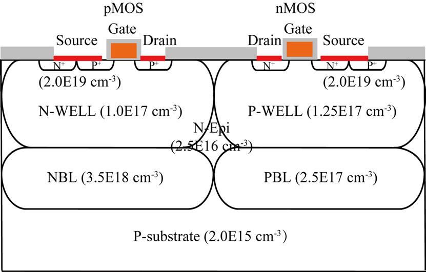
Figure 2. The schematic cross-section of the CMOS.
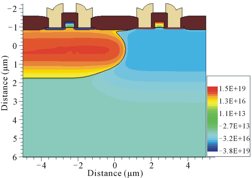
Figure 3. 2D cross-section of CMOS.
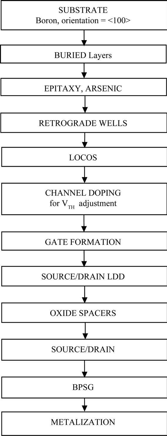
Figure 4. The process steps of a 0.35 µm BiCMOS technology.

Figure 5. nMOS and pMOS; e.g. Id-VdS characteristics.
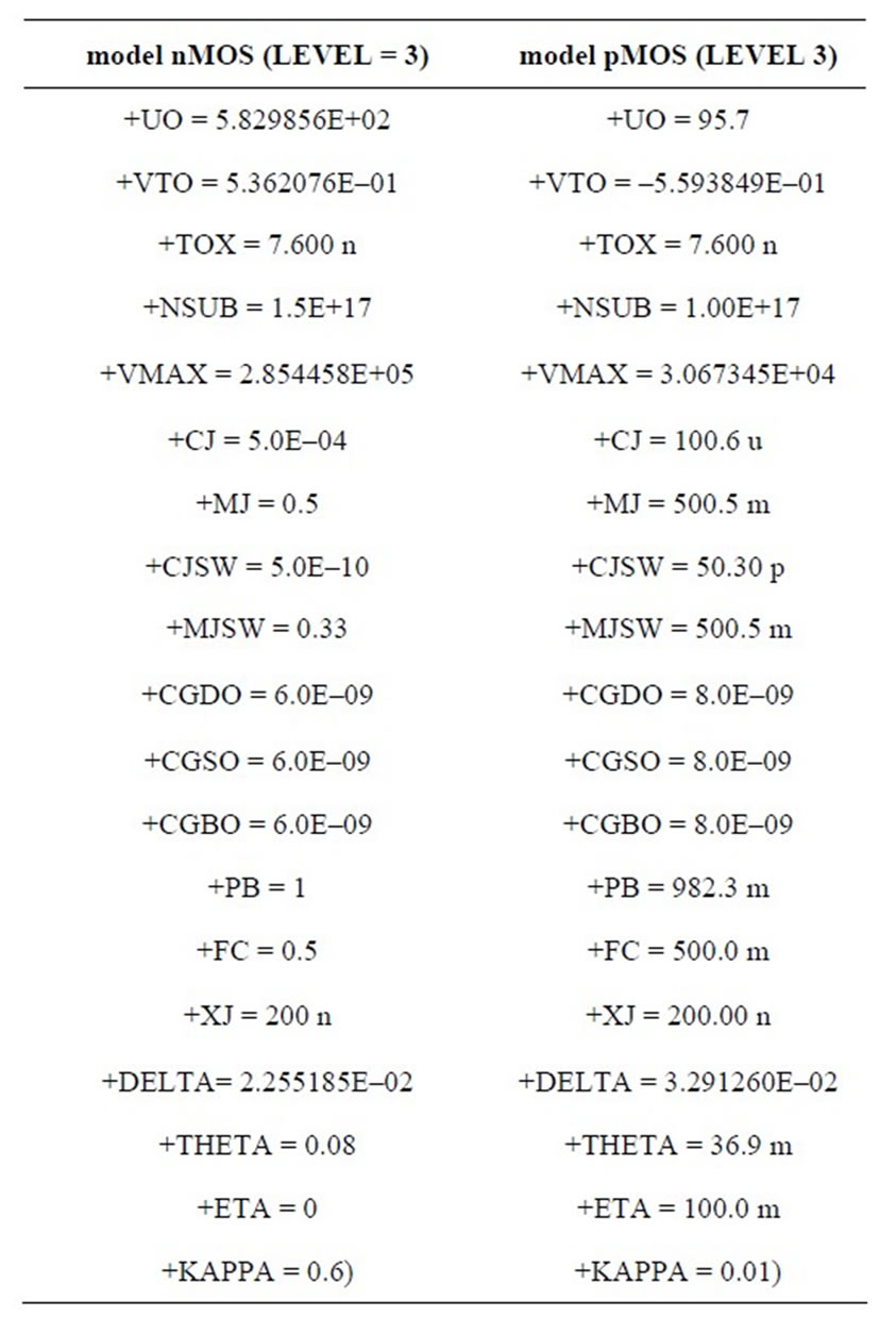
Table 1. The SPICE model parameters of CMOS devices.
is supposed as shown in Figure 6(a). The potential distribution in the TSV-CMOS structure is shown in Figure 6(a); it is clearly observed that nearly half of the TSV voltage is dropped across the TSV oxide (at the left) and the other half across the depleted region in the substrate and there is a few potential contours are observed in the active regions of the MOS devices. The waveforms of the TSV, CMOS input and output voltages and the output current wave form (the current through the load capacitor) are shown in Figure 6(b). It is cleared from the figure that the current is switching w.r.t the CMOS input waveform and there is no effect of the digital HV signal of the TSV.
In order to accelerate the devices and circuit design without significant loss of accuracy and reliability, designer should not model the substrate with numerical methods.
Especially in the high-frequency cases, the loss of the circuit performance caused by the silicon substrate is very important. Considering the radio frequency (RF) range, the substrate could have, at some nodes of interest, an “RLC” behavior (approximately an “RC” one for low frequencies); it is important to prevent the whole system
 (a)
(a)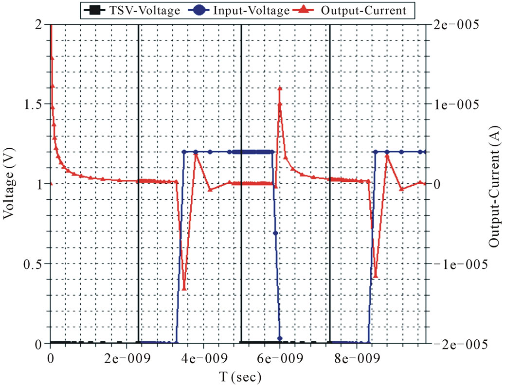 (b)
(b)
Figure 6. (a) The Potential distribution, and (b) the voltages and output-current waveforms for Vin = 0.0/1.2 V and VTSV = 0.0/42.0 V.
(die, with its packaging) from surges, bounces, or parasitic oscillations. So we need effective tools to analyze the practical layout, to calculate the electric performance of the circuit. We need calculate the impedance matrix and partial inductance matrix to analyze the substrate coupling.
Here, Green function will be applied for homogeneous layers to the substrate circuit model extraction, as opposed to numerical method; the resolution speed of this method is much faster. Some basic recalls and concept are first introduced. The use of discrete cosine transforms (DCT) or Fast Fourier transforms (FFT) in this model will accelerate the compute speed obviously. Then an improved model which can be applied on substrate with in-depth contacts is shown; it can treat the case of contacts lying in different layers. As a check, we compare with a FEM method [6].
3. Substrate Extraction
3.1. Green Kernels
In this paragraph, we present a technique for modeling the substrate. This algorithm relies on the electrostatic Green function in the substrate medium and the Fast Fourier Transform; it is well known when contacts are on the die surface [7,8].
Green Function and Poisson’s Equation [9,10]
Posing and solving problems that are described by the Poisson equation is one of the cornerstones of electrostatics. Poisson’s equation is handled as:
 (1)
(1)
where, V is the electrical potential, ρ is the charge density and ε the dielectric permittivity of the medium.
The algorithm is the same for the electrostatic or quasi-static case where Poisson’s equation is replaced by the Ohm’s Law (neglecting the diffusion currents):
 (2)
(2)
with , for the harmonic domain.
Where, J is the current density in A∙m–2, E the electric field in V∙m–1 and σ the conductivity of the medium in S∙m–1. A different form of the law’s ohm is given by:
 (3)
(3)
where V is the potential (V), div(J) is not null since an extent current (density) is imposed.
Finding V for some given  and ε is an important practical problem, since this is the usual way to derive the electric potential for a given charge distribution.
The above equation may be turned into an integral equation of the form:
 (4)
(4)
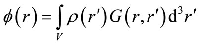
G is the potential due to a point charge placed at a point r' and G is known as Green function (or Kernel).
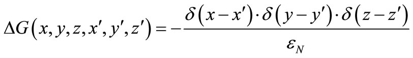
The Green function can be got by solving the following equation:
 (5)
(5)
If the Green function is known, this equation does provide a technique for determining the potential at any point in the volume V due to a known arbitrarily distributed charge density.
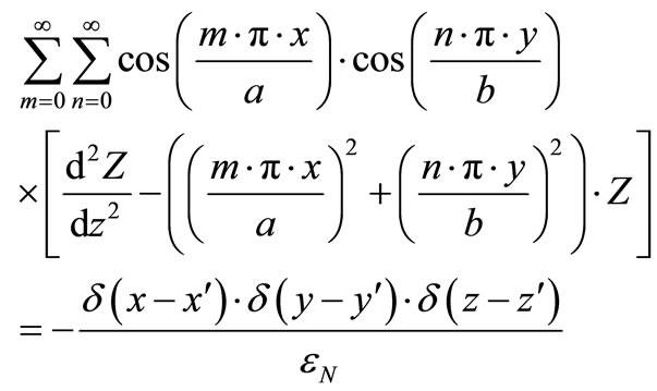
Consider a localized charge at the point P (x', y', z') in the upper layer of stacked dielectric layers as shown on the Figure 7(a). Here, we assume the substrate as an equivalent system composed of stacked layers; each of them has a dielectric constant and a resistivity of the corresponding resistive substrate layer.
The potential in Q (x, y, z) induced by the charge in P is the solution of Poisson’s equation and is given by:
 (a)
(a)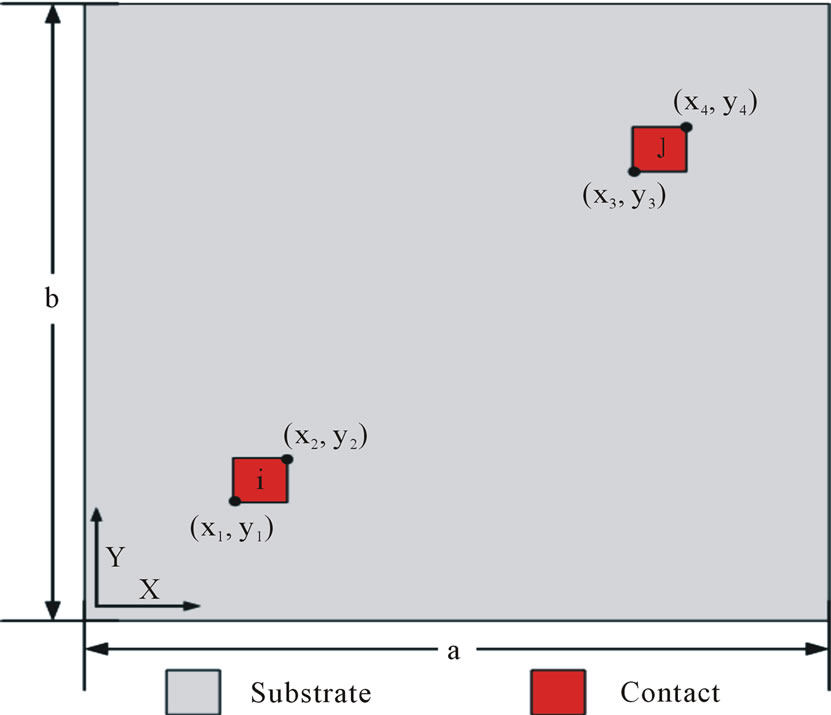 (b)
(b)
Figure 7. (a) Stacked layers model of the substrate and (b) Top view: contact altitudes: –d < zi, zj < 0.
 (6)
(6)
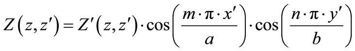
If we assume that G = X (x, x'). Y (y, y'). Z (z, z'), we can rewrite the Poisson’s equation, thus resulting in:
 (7)
(7)
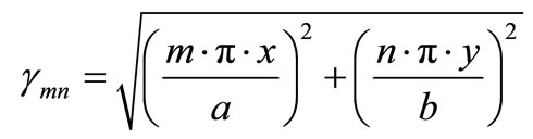
Noting a and b the die dimensions, we get:
 (8)
(8)
(m and n are integers)
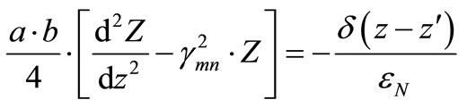
The Green’s function-equation-involves an infinite series of sinusoidal functions:
 (9)
(9)
By defining:
 (10)
(10)
we get a simple equation:
 (11)
(11)
 .
.
For z ≠ z', δ (z – z') = 0. The above equation has the well known general solution:
 (12)
(12)
This equation invokes a transmitted wave and a reflected one. Then, after deriving formal mathematical solution for Equation (12), with boundary conditions, we will discuss hereafter on a more physical approach of the problem, using the so-called Transmission Lines Method (TLM).
A general solution, for m > 0 and n > 0 of the Green electrostatic function is given as:
 (13)
(13)
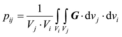
Then we can get, or instance, the expression of the capacities from the matrix of capacitive coefficients [C] by using this equation. In order to have [C] or [G] (conductance matrix), we only have to calculate [P], i.e.:
 (14)
(14)
Now, the Green function becomes the only unknown. As long as we get G, then the contact-to-contact capacitance (or admittance) will be easily calculated.
Here we only consider the case of both the point charge and the point of observation are in the same dielectric layer, on the surface with z = z' = 0. The Green function then changes to,
 (15)
(15)
where Cmn = 0 for (m = n = 0), Cmn = 2 for m = 0 or n = 0 but m ≠ n and Cmn = 4 for all others mn (m > 0) and (n > 0).
The function fmn is given by:
 (16)
(16)
where
 (17)
(17)
βN and ΓN can be computed recursively from:
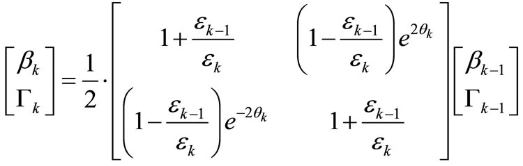 (18)
(18)
where .
.
Substituting by the Green function and considering two rectangular contacts i and j whom the geometric data are given by x1, x2, y1, y2 and x3, x4, y3, y4.
The “coefficient-of-potential” matrix is calculated with the following equation, giving the potential of contact i, induced by an elementary charge spread all over the contact:
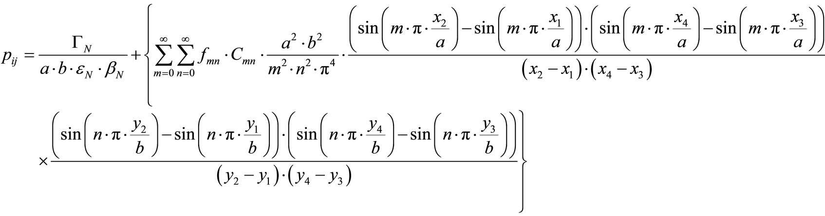 (19)
(19)
And then we invert [P] to generate [C] and extract contact-to-contact parasitic.
In practice, we adjoin a new calculation grid to the initial one (of a M·N dimension), in such a way that we can apply directly a discrete cosine transform (DCT) to accelerate the algorithm resolution.
To calculate the substrate resistance, the Green’s method is formally equivalent. We have only to replace ε by 1/σ (= ρ) in the former analytical expressions and to consider the admittance matrix [G] replacing the capacitance matrix [C] to determine the different substrate resistances. A current spreading along all the contact is then consider instead of a Q (charge).
For instance, stating from some region of interest of the 0.35 µm CMOS technology cited above, first we approximate the actual profile by uniformly doped stacked layers.
3.2. Transmission Line Analogy for Multilayered Media
In its simplest form, a transmission Line (TL) is a pair of conductors linking together two electrical systems (source and load, for instance), with a forward (f) and return (r) paths; for cases where the return path (and the forward) is floating, a third conductor (or more) is introduced as the grounding shield. For microwaves, they are waveguides. In our case, the propagation of EM waves, their interferences, through the silicon substrate, is among the most serious obstacles in the steady trend towards integration of present day microelectronics. In fact the TL method (TLM) is well established; it can be seen as a more physical interpretation of the mathematical developments presented above, but equivalent.
The principal strength of this method is it is well dedicated to embedded contacts, in any number; for instance in Figure 7(b), keeping the same location of the contacts in the < x, y > plane, we have been changing ad libitum their zi and zj contact altitudes. In practice, a region of interest of the 0.35 μm process is selected, and decomposed in twelve layers (see Figure 8 and Table 2).
Let us consider a plane wave, which its plane of incidence parallel to the
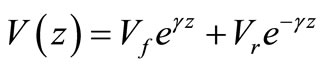
Then, we consider the general case in which the line’s impedance is not the same as that of the load. Wave front A hits the load ZL: a part of its energy is absorbed by ZL, the remaining energy is reflected; in this case, voltage and current wave-fronts are not in phase. This reflected wave can meet another incident wave form B.
The direction of current flow depends on the polarity of the waveform at the time of observation; if two positive directed waveforms (one forward an one reflected) meet, the current waveforms subtract but the voltage
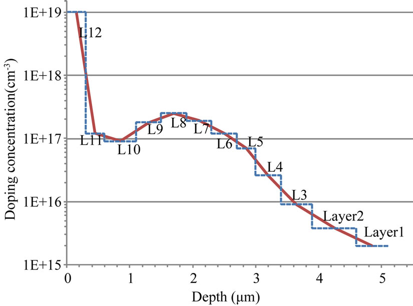
Figure 8. A specific depth profile of the 0.35 μm technology (p-region).

Table 2. Schematic doping profile values in the default pregion of the standard BiCMOS process.
waveforms add. Likewise, if a positive directed waveform meets a negative directed waveform, the current will add and the voltage will subtract (Figure 9).
The expression for the apparent impedance is given below:
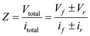 (20)
(20)
staring for the general solution for voltages and currents:
 (21)
(21)
 (22)
(22)
where the propagation coefficient is the square root of Z

Figure 9. Two possible interactions between the voltage (current) of the forward wave and the voltage (current) of the reflected wave.
and Y product, respectively the linear impedance and admittance;
The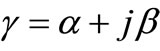 ;
; ![]() attenuation,
attenuation,  = 360°/λsi are derived directly from the chain matrix:
 (23)
(23)
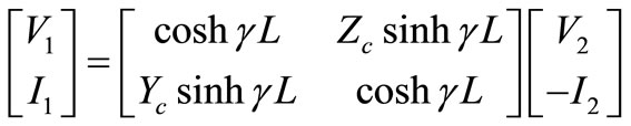
and from the output branch: V2 = –ZLI2
 (24)
(24)
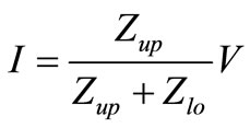
where Zc = 1/Yc (square root of Z and Y ratio) is the characteristics impedance (Electric and magnetic fields modulus ratio), ZL is the charge impedance, L is the distance from the load. We can extract an input impedance, said Zl (= V1/I1), function of the load impedance Zl+1 (l: layer number) as:
 (25)
(25)
This very well known (TLM) equation Zl is directly related to Equation (16).
In fact, restarting from Equation (12), taking into account the limit or boundary conditions—continuity of potential, and the discontinuity of the electric field if there is a surface charge at the considered layer interface —it is quite easy to program this iterative solution (versus substrate depth, or layers) of Equation (12).
Regarding the injected current source point (contact), there are two classes of layers, upper (up) and lower (lo) ones. Then we introduce in our program [11] the derivation current (for instance, in the upper layer):
 (26)
(26)
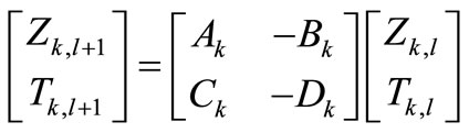
In our simulator, we use a matricial formalism, extending the impedance and the current transmission from a layer l to its adjacent (cf. Equation (16) or Equation (25)), starting from a k layer:
 (27)
(27)
4. First Green/TLM Results
First of all, we did some numerical experiences using COMSOL® [6], a well known multiphysics (cf. thermal, mechanical couplings) simulator; it is also a dedicated tool for full wave electromagnetic analysis. It uses essentially Galerkin-like algorithms. Typically a 3D simulation can use a few ten of minutes or hours.
For instance, we compare it, with a very good accuracy, with the analytical formula associated to an “R//C” filter (see, for instance: Figure 10; Resistivity bulk: 10 Ω∙cm, 2 contacts: 50 × 50 µm2, distant of 200 µm); we obtain the following extracted parameters: R = 2.3 KΩ, C = 4.5 fF.
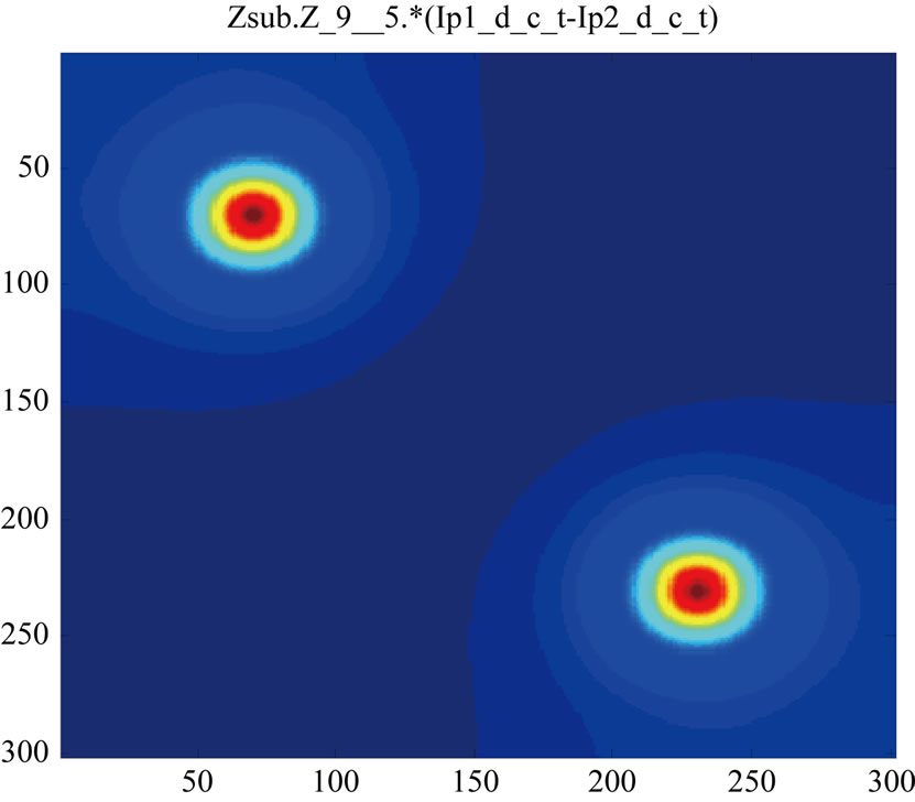
Now it is very easy to calculate, by TLM method any transfer impedance. Possibly embedded in the substrate, contacts can be introduced into any layer; they can be real (metal like) or virtual. Presented is a two contacts example on the Figure 11; the he surface die is 30 μm × 30 μm, with M = N = 300, surface contact: 20 points × 20 points (the calculation point, M·N, are equidistributed).
The Green function G(z, z') describing the electric field response to the unity current is identifiable to the transfer impedance between any two points; then we can calculate this impedance spreading. We can extract the potential, particularly between two contacts. This way, we use the inverse transform of the Kroneker matricial product of the impedance by the current DCT. For instance, as a first check, we present on the Figure 12 the impedance module for two in-depth contacts, at the interfaces: L5/L6 and L9/L10; the comparison between “TLM/Green” and “COMSOL” is quite good.
5. Conclusions
An efficient and elegant technique to model substrate coupling, via frequency dependant impedance extraction,
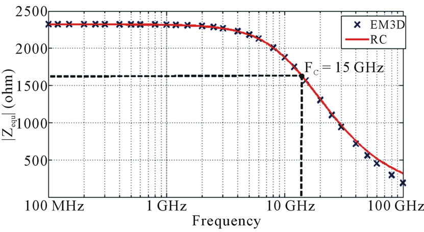
Figure 10. Impedance: comparison between COMSOL and the analytical result “R//C” (Resistivity bulk: 10 Ω∙cm; 2 contacts: 50 × 50 µm2, distant of 200 µm).
 (a)
(a)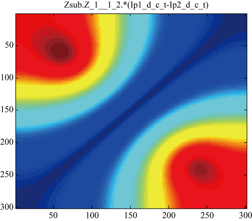 (b)
(b)
Figure 11. Potential distributions via transfer impedance (from red to dark blue: voltage decreasing). (a) Contacts embedded in the bulk; interfaces: L5/L6 and L9/L10; (b) Contacts at surface and bottom.
has been presented and programmed. The technique uses a combination of the classical Green function or transmission line method approach and the use of Fast Fourier Transform. The speed of this latter technique makes it suitable for optimization of circuit layout and for minimization of substrate coupling related effects. But the model is often limited to contact locations at the surface; in practice, in our work, the contacts can be placed anywhere in the substrate, so a new research should be enhanced in 3D.
For the near future, considering for instance our compatible 0.35 μm CMOS predilection technology, the digital part can attack any region from the substrate, the ana-
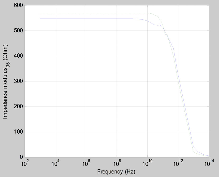
Figure 12. Comparison between finite element method (dashed-upper-line) and Green/TLM (solid-lower-line) (layer interfaces: L5/L6 and L9/L10).
logical CMOS or HBT devices, via a stochastic probability matrix derived from the switching activity [12]; the parasitic wave or impulsion aggressions can be derived via our transfer impedance methods; In fact, we could calculate a two point spectral density of current fluctuations, knowing that our method can handle any number of contacts. The ultimate goal will be to build a “whole” compact model dedicated to actual 3D circuits.
6. Acknowledgements
This work is supported by the Cluster for Application and Technology Research in Europe on NanoElectronics (CATRENE): 3D-TSV Integration for MultiMedia and Mobile applications (3DIM3).
REFERENCES
- L. Cadix, C. Bermond, C. Fuchs, A. Farcy, P. Leduc, L. DiCioccio, M. Assous, M. Rousseau, F. Lorut, L. L. Chapelon, B. Flechet, N. Sillon and P. Ancey, “RF Characterization and Modelling of High Density Through Silicon Vias for 3D Chip Stacking,” Microelectronic Engineering, Vol. 87, No. 3, 2010, pp. 491-495. doi:10.1016/j.mee.2009.08.026
- R. Gharpurey and S. Hosur, “Transform Domain Techniques for Efficient Extraction of Substrate Parasitics,” International Conference on Computer-Aided Design, San Jose, 9-13 November 1997, pp. 461-467. doi:10.1109/ICCAD.1997.643576
- P. S. Crovetti and F. L. Fiori, “Efficient BEM-Based Substrate Network Extraction in Silicon SoCs,” Microelectron Journal, Vol. 39, No. 12, 2008, pp. 1774-1784. doi:10.1016/j.mejo.2008.07.034
- M. Abouelatta-Ebrahim, R. Dahmani, O. Valorge, F. Calmon and C. Gontrand, “Modelling of through Silicon via and Devices Electromagnetic Coupling,” Microelectronics Journal, Vol. 42, No. 2, 2011, pp. 316-324. doi:10.1016/j.mejo.2010.10.017
- W8511BP IC-CAP Wafer Professional Measurement Bundle, Agilent.
- COMSOL Multiphysics. http://www.comsol.com
- R. Gharpurey and R. G. Meyer, “Modeling and Analysis of Substrate Coupling in Integrated Circuits,” IEEE Journal of Solid State Circuits, Vol. 31, No. 3, 1996, pp. 344-353. doi:10.1109/4.494196
- A. M. Niknejad, R. Gharpurey and R. G. Meyer, “Numerically Stable Green Function for Modeling and Analysis of Substrate Coupling in Integrated Circuits,” IEEE Transactions on Computer-Aided Design of Integrated Circuits and Systems, Vol. 17, No. 4, 1998, pp. 305-315. doi:10.1109/43.703820
- N. Verghese, D. J. Allstot and S. Masui, “Rapid Simulation of Substrate Coupling Effects in Mixed-Mode ICs,” IEEE Custom Integrated Circuits Conference, San Diego, 9-12 May 1993, pp. 18.3.1-18.3.4. doi:10.1109/CICC.1993.590746
- N. K. Verghese, D. J. Allstot and M. A. Wolfe, “Fast Parasitic Extraction for Substrate Coupling in Mixed-Signal ICs,” IEEE Custom Integrated Circuits Conference, Santa Clara, 1-4 May 1995, pp. 121-124. doi:10.1109/CICC.1995.518149
- Matlab. http://www.mathworks.com
- C. Gontrand, S. Labiod, O. Valorge, P. Mary, J. C. N. Perez, P. J. Viverge, F. Calmon and S. Latreche, “Markov Chain Approach of Digital Flow Disturbances on Supplies via Heterogeneous Integrated Circuit Substrate,” International Journal of Numerical Modeling, Vol. 30, No. 4, 2010, pp. 54-63. doi:10.2316/Journal.205.2010.2.205-4999.