Journal of Modern Physics
Vol.4 No.3(2013), Article ID:28566,5 pages DOI:10.4236/jmp.2013.43041
Spin Transfer in EuO:Fe/GaAs Contact
Russian State Vocational Pedagogic University, Ekaterinburg, Russia
Email: A.S.Bor@rsvpu.ru
Received August 30, 2012; revised January 25, 2013; accepted February 5, 2013
Keywords: Spintronics; Magnetic Semi-Conduction; Spin Transfer
ABSTRACT
Spin-wave structures whose current-voltage characteristics are controlled at room temperatures by magnetic field were produced with industrial technological methods using a spintronic europium-monoxide-based thin-film composite as an emitter and monocrystalline semiconductor n-GaAs as a collector. This shows that spin current transport actually exists and that a high-temperature spin transistor was produced with the use of the magnetic semiconductor/nonmagnetic semiconductor contact.
1. Introduction
Until now one of the most difficult problems in semiconductoring spintronics is the realization of stable spin current transport at room temperatures and creation of a spin transistor on the basis of the ferromagnetic semiconductor/nonmagnetic semiconductor contact (FS/S). So far all available achievements in this field of microelectronics have to do with low temperatures. The operating temperatures of spin diodes are confined at best within 150 - 180 K [1-3]. The same limiting temperatures are characteristic of the spin transistor developed by Appelbaum et al. [4,5], who realized tunneling of spins through a micron-thick silicon base. As is known, spin injection was from a ferromagnetic metallic alloy Co-Fe, and, considering the values of electrical resistivity of the barrier layer (interface) in the FS/S contact, this resistor can only with great reserve be referred to semiconducting electronic devices. Besides, spin transport was directed to silicon, a nonmagnetic semiconductor, which is not a very suitable base for a spin transistor to implement the logical functions of spin informatics because of its narrow-band forbidden gap and a g-factor too small for charge carriers. Production of low-temperature FS/S spin structures verified by practice and requirements to parameters of spintronic semiconducting systems formulated earlier [6] substantiate spintronics as microelectronics of Zeeman electronic levels, which considerably restricts to date the choice of the basic nonmagnetic semiconductor-a spin collector. These are mainly InSb, GaAs, and GaN crystals having a g-factor of ~50, which were not however widely applied in modern microelectronics based on the Si base. Moreover, the technology for the production of such crystals with pre-assigned concentration of carriers in them in many respects is lagging behind that developed for silicon.
The requirements to ferromagnetic semiconductors as injectors (emitters) of electronic spins in spintronic devices are rather simple. Their Curie temperatures should be higher than room temperatures. It is desirable that the value of magnetization be considerable enough to ensure a high degree of spin polarization of carriers in the FS itself (enhanced energy of splitting of FS spin subbands). Specific electrical resistance of the injector material and the base (detector) should have similar values to ensure interface transparency for tunneling spins. And, certainly, adaptability to streamlined production: easy synthesis of materials including those in the form of thin films and possibility of production of spintronic heterostructures with the above semiconducting crystals.
It happened so that all familiar “classical” single-phase FS are low-temperature ferromagnetics—their Curie temperatures are below ТC ~ 130 - 140 K. Several phases based on manganese lanthanides, whose ТC are as high as ~350 K, are the exception. However, it is rather doubtful to refer the latter materials to monophase single-sublettice ferromagnetic crystals since they (like other LaMnO3- based phases) always contain a certain amount of Mn+4 (or Mn+2) ions, which form a sublattice with antiferromagnetic order with respect to the lattice on the basis of Mn+3 ion spins. Apparently, for this reason no stable spin transition with participation of such FS phases was hitherto observed even at low temperatures.
There is a series of diluted magnetic semiconductors (DMS) with ТC above room temperatures, whose magnetism is also connected with the sublattice based on Mn+3 ions. They are widely applied in spintronics and were used in many low-temperature contacts [7]. However, such phases belong rather to weak ferromagnetic materials and were not so far reported to be used in any working spin structures. Co2MnSn-type ferromagnetic semimetallic Heusler alloys with ТC ≥ 500 К used as spin injectors also failed to increase the above operating temperatures of spin diodes.
Therefore the search for and creation of materials for spin injectors involved recently the designing of composites on the basis of high energy-gap semiconductors of metal oxides (ZnO, TiO2, SiO2, etc.) containing an impurity of a ferromagnetic metal-Fe or Co [8]. When the metal content is small (much smaller than the percolation limit), such composites remain semiconductors and become ferromagnetic materials with ТC values, which are considerably higher than room temperatures. According to their specific magnetization values, such composites can be also related to weak ferromagnetics; this, however, does not exclude their application in high-temperature spintronics. In addition, interfaces on their basis may have gigantic magnetoresistance effects [9].
In view thereof, of particular interest for spintronics are ferromagnetic composites based on the “classical” FS-europium monoxide (EuO) with proper Curie temperature ТC = 69 К. At Т = 0 К this oxide exhibits a record for ferromagnetics saturation magnetization 4πМ = 2.4 T, which corresponds to the magnetic moment of Eu+2 ion equal to 7μB (cf.: the maximal value of this parameter achieved for DMS is 4πМ = 0.75 T, while for composites based on transition metal oxides 4πМ = 0.10 T). At the same time current carriers in EuO possess an almost 100% spin order—the spin subband for antiparallel spins is empty. That is why at low temperatures EuO may have spin injection of the same order.
Considering these parameters, the monophase solid solutions Eu1-xRxO (R-La, Gd, Sm), whose ТC are increased to 120 - 130 K owing to magnetic heterogeneity effect and exchange between magnetic quasi-molecules [10], may be comparable to a certain extent with EuO. It is true that the energy of spin subbands splitting and the degree of spin polarization of charge carriers decrease slightly for these species. By alloying of EuO, its specific electrical resistance and the concentration of electronic charge carriers can be varied in a wide range from the values typical of semiconductors to those of semimetals. This ensures transparency of interface for contacts with nonmagnetic semiconductors. Efficiency of such crystals in low-temperature spin devices was demonstrated in [1].
2. Experiment Data
In order to retain the above positive features of EuO, earlier we synthesized a series of EuO-Fe(Co) composites, including those in the form of nano-sized films, whose Curie temperatures corresponded to transition ferromagnetic metals, while the composites remained semiconductors with forbidden gap width Eg ≈ 0.75 eV and specific electrical resistivity at room temperatures within ρ ≈ 1 ÷ 10 Ohm·cm [11]. The value of specific magnetization of these composites at room temperature is М = 60 emu/g, which is an order of magnitude (or sometimes more) greater than for all the other mentioned above oxide composites and DMS proposed as spin injectors for spintronic structures. This value of М is likely to be due not only to the share of ferromagnetic Eu2+ ions, but also to their partial spin polarization in the vicinity of the impurity iron ion, which leads to the formation of Eu+3-Fe+ -O−2 clusters. Such clusters arise in the composite structure as a result of spin transport by the indirect d-f exchange mechanism proposed for such composites in Ref. [12]. This is confirmed by direct magnetic measurements and Mössbauer spectroscopy results [13,14]. According to these data, specific magnetization of the composite in the region of Т ≈ 480 K exhibits an inflexion with a peak at DМ ≈ 10 emu/g, which is similar to the magnetic phase transition associated with disordering of the above clusters. NGR 57Fe-spectra of the composite contain at least two sextets of Zeeman lines: one sextet with Нeff = 32.8 Т, isomeric displacement δ = 0, and quadrupole splitting ε = 0, the other sextet with Нeff = 19.2 Т, δ = +0.20 mm/s, ε = 0.005 mm/s, which are attributed to free α-Fe particles in the composite and in the above clusters, respectively [13]. The relative intensity of their sextets (I(α-Fe) ≈ 0.72; I(EuO/Fe) ≈ 0.28) shows that the part of impurity iron atoms, which entered into chemical contact with europium, is relatively small in comparison with the whole level of alloying of EuO (about 1/3 of 25 weight % Fe). Mössbauer spectroscopy on 151Eu nuclei [14] also points to a considerable part of paramagnetic ions Eu3+ in the composite.
The aforesaid was the basis for creation of a spintronic device capable of spin transport at room temperatures—a high-temperature field-effect spin transistor based on the nonmagnetic semiconductor GaAs used as a collector [15]. This constitutes the main aim of the present work.
Creation of a field-effect transistor based on the (EuO: Fe)/GaAs contact was a three-stage process, in which industrial microelectronic technologies were employed for designing of such devices and for production of integrated circuits. At the first stage, rectangular 30 × 0.2 mm2 channels were etched in a monocrystalline n-GaAs plate with the concentration of carriers n ≈ 1014 cm−3 using lithography methods, which were filled with a ≈ 400 nm thick layer of gold. The Au layer was covered with a protective SiOx layer (40 nm), which served, together with the Au contact, as a Schottky barrier and a transistor base. Over this layer, there was applied a 0.2 μm thick composite (EuO:Fe) layer, which served as a spin emitter (injector). The contacts to the emitter and the detector were made of gold.
Magnetization and the current-voltage characteristic of some contact structures were measured at room temperature. From Figure 1 it follows that magnetization of a structure becomes saturated in the fields higher than 0.5 T. The magnetization loop in the magnetic easy direction was more rectangular than in the hard direction. But on the whole the difference was insignificant. The magnetization loops were not found to open within the magnetometer detection limit. Upon saturation, the proper value of the magnetic moment of the structure was in the region of М ≈ 40 emu/g.
The current-voltage characteristic of the contact structure is presented in Figure 2 in the absence of external magnetic field and in the magnetized state in the field Н = 200 mT. When no external magnetic field is applied and the emitter is not magnetized, this characteristic is typical of a field-effect MOS transistor. If the emitter is magnetized, the current in the collector appears already at the zero bias on the base, and its value is smaller than that at Н = 0. In other words, it is determined by the spin component of tunnel current, which coincides with the direction of magnetization of the emitter—the spin injector. When bias voltage is applied to the base, the value of spin current decreases too.
3. Discussion
If the collector current in a non-magnetized emitter is considered as 100% charge transport (J0), than the degree of spin transport (Р) can be evaluated from the charge transport of the magnetized emitter (Jm) as:
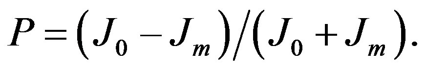
According to Figure 2, Р ≈ 60%, which is a rather high value determined in many respects apparently by the EuO component of the composite—the spin emitter. This result, as well as the enhanced magnetic moment of
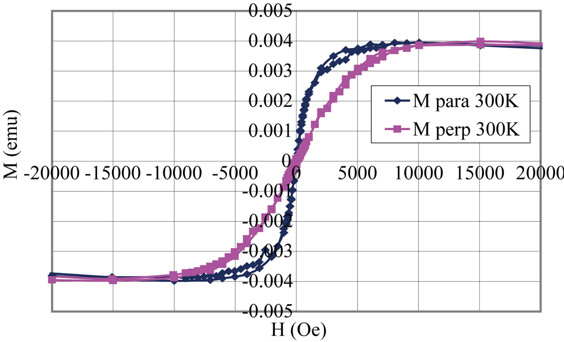
Figure 1. Magnetization curves of (EuO:Fe)/GaAs contact along (magnetic easy direction, para) and perpendicular to the contact plane (magnetic hard direction, perp) at room temperature.
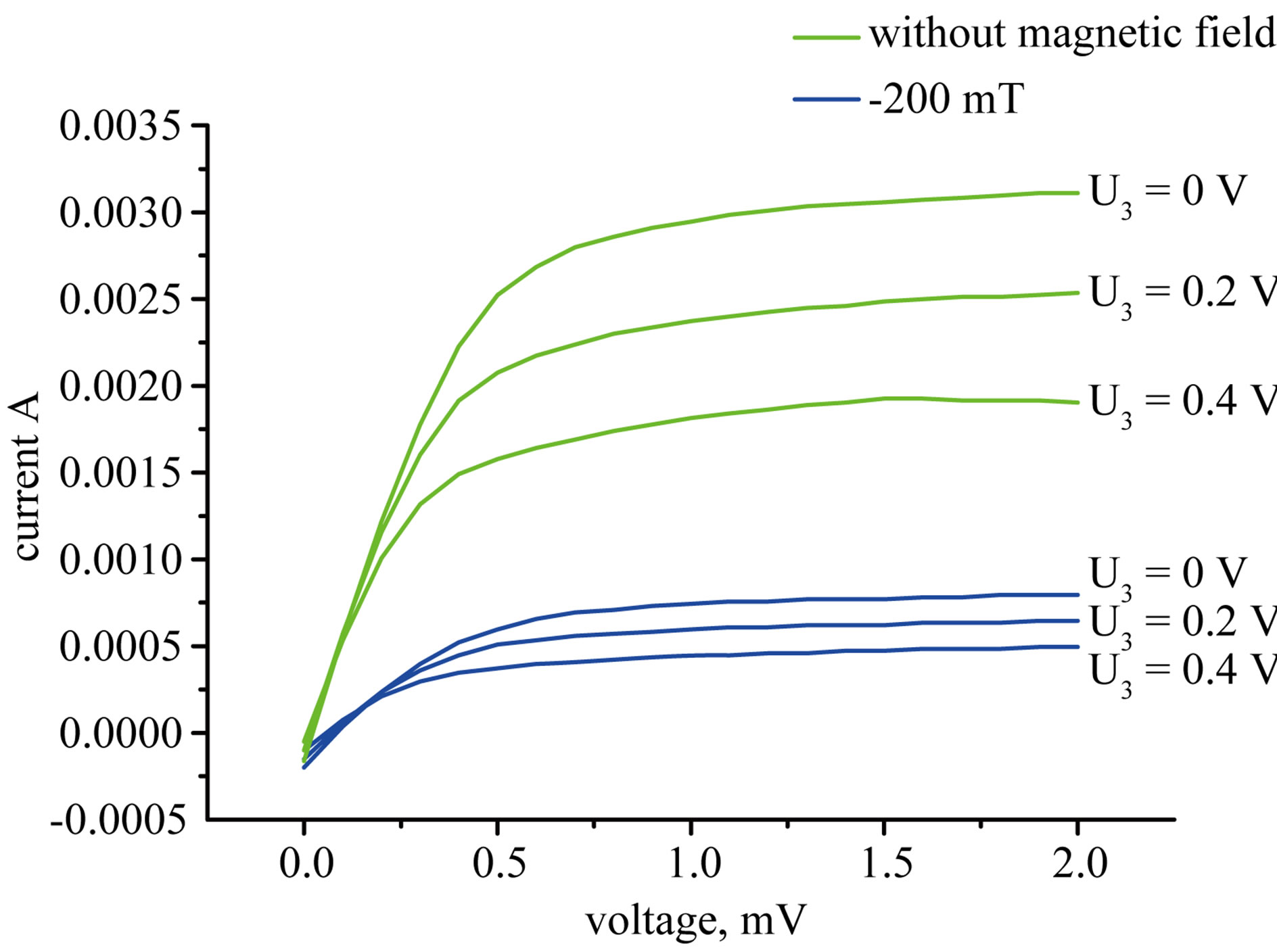
Figure 2. Current-voltage characteristics of spin transistor without magnetic field and in the magnetic field of 200 mT (2 kOe).
the emitter as compared with pure Fe at room temperature and the above mentioned NGR data on 57Fe nuclei show that the presence of α-iron nanoparticles and of the iron partially bound in Eu-Fe-O clusters actually leads to electronic density transfer from Eu2+ ions to iron and to certain recovery of spin polarization of Eu3+ ions in the vicinity of impurity Fe+ ions in the cluster up to 480 K. In its turn, this determines enhanced spin polarization of current carriers injected from such an emitter to a nonmagnetic semiconductor.
The mechanism of injecting of spin-polarized electrons from this emitter through the oxide Schottky interface with a nonmagnetic semiconductor-GaAs collector and their further transport in it is simulated on the detector circuit of the FS/S contact (Figure 3) [6]. It is true that in our case the current-voltage characteristic of the spin transistor was registered at room temperatures, while P < 100%.
Possibility of direct spin transport realization of the current carriers from FS to the upper Zeeman level of the nonmagnetic semiconductor in electric field. This spin transfer is due to the positive sign of the spin s-d (d-f) exchange integral between the magnetic moments of the carriers in the FS. In the case of the predominance of the negative sign of the exchange interaction between the spins of the carriers in the injector, transfer through the contact area on the lower Zeeman level in the forbidden band of nonmagnetic semiconductor and its occupation are possible.
In both cases, effects, obliged only to energy absorb, must be observed. Same preferential occupation of only upper Zeeman level in the first case corresponds to the absorption of energy with the reduction of EPR signal intensity. The transition of the carrier on the EPR frequency on unoccupied lower Zeeman level of the semiconductor and its population of electrons is accompanied
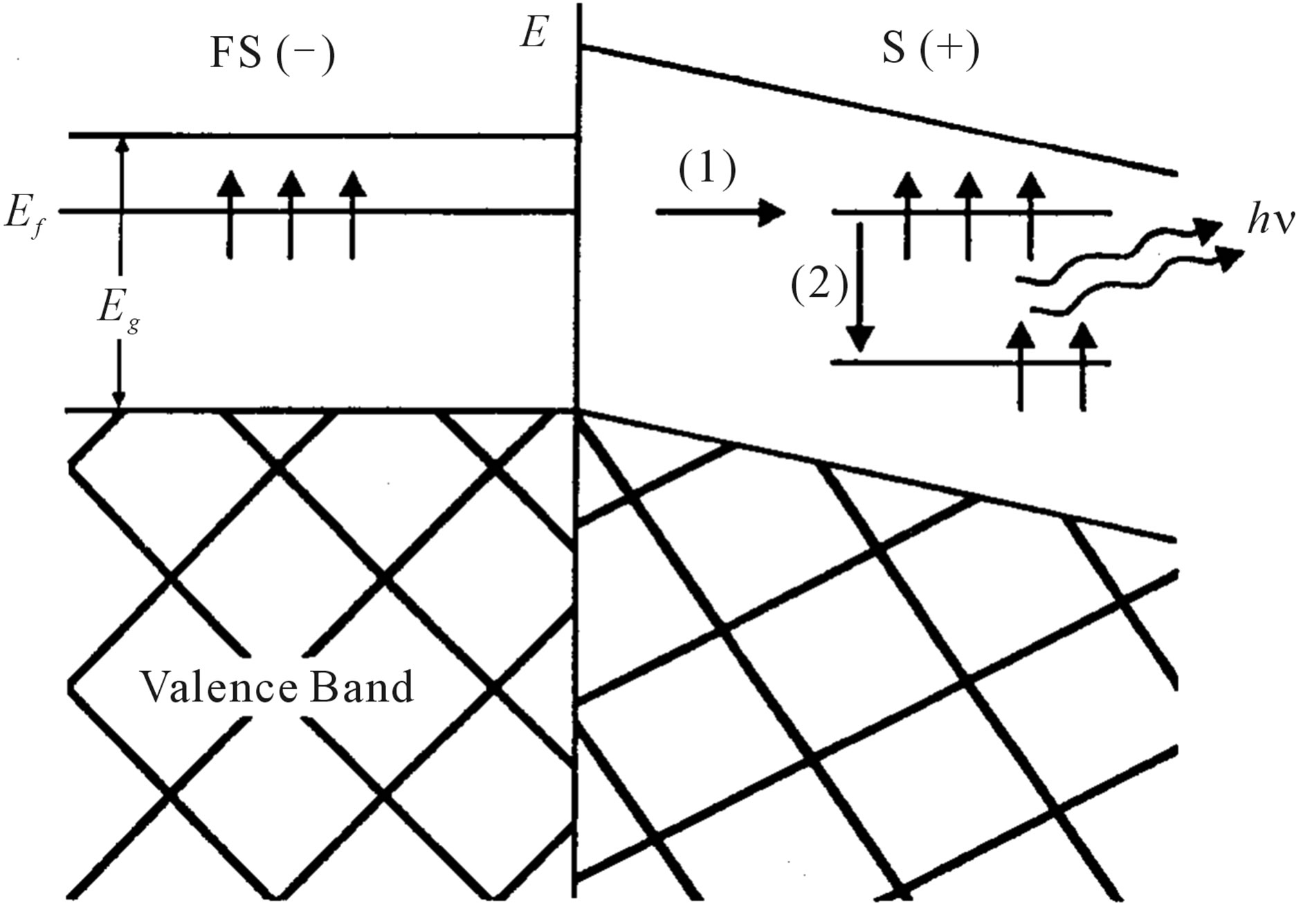
Figure 3. The zone scheme of the FS/S contact: 1-the process of irradiative spin tranfer by the carrier from FS to the upper (donor) Zeeman level of nonmagnetic semiconduction with the increasing occupation density without variable h-field; 2-carriers’ transfer to the unoccupied lower (acceptor) Zeeman level S with the EPR frequency ang radiation generation from S. Ef-is Fermi level of FS, which is splitted into sublevels with spin orienation (↑) and empty (↓) by the spontaneous magnetization.
by increasing level of the ESR signal intensity and by the ejection of appropriate energy hn (the generation process of radiation from S).
In our case, with the smaller value of P < 100% a part of the spin carriers will have another orientation and will be located on the upper split sublevel Ef-with the preferred spin orientation of the carriers against the magnetization (↓). This would correspond to the presence of partly negative exchange between current carriers. In this case, current transport through the FS/S-barrier will be irradiative again and will correspond the occupation both upper and lower Zeeman levels in S.
Assuming that electromagnetic radiation occurs at a EPR-semiconductor frequency with the electron passage through the barrier of the FS/S to the upper Zeeman level of the semiconductor and its further transition to an unoccupied lower level with the emission of an energy quanta, then theoretically permissible limit output radiation of such heterostructure would be a value:
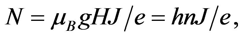
where μB is the Bohr magneton, Н is the external magnetic field, J-the current flowing through the heterostructure, e-electron charge. Its evaluation for conventional parameters of the waveguide channel and for the crystal n-InSb gives us the following values: for the 8-mm range N = 156 mkW/A, and for the 0.1 mm range-N = 12 mV/ A.
In the case of equiprobable occupation of the upper and lower Zeeman levels in S by the electrons from the partially filled zones FS with the spins (↑) and (↓) there would not be the radiation from the S. However, the reverse current from the S to the FS in the heterostructure at the interface for spins (↓) an additional energy barrier with the value D = 2 As (where A is exchange parameter, s-spin of Eu2+ ion) must occur. This barrier forms some sort of barrier layer and the growth of the reverse contact electric resistivity—in the FS only carriers with spin (↑) will take place. Such FS/S-heterostructure can manifest itself as a spin filter.
4. Conclusion
Thus, the use of the ferromagnetic semiconducting composite EuO:Fe as an emitter of a field-effect transistor in contact with the nonmagnetic semiconductor GaAs allows one to create a high-temperature spin transistor, the operating characteristics of which are controlled by external magnetic field. The degree of spin polarization of current carriers in it may be very high. Since the enhanced g-factor of spin current carriers of the collector ensures considerable (in energy) splitting of Zeeman electronic levels in the forbidden band defined as D = μB·g·H, than the proposed device can be the basis for the development of a whole series of spintronic systems. According to estimates for an n-InSb crystal, whose physical characteristics are similar to those of n-GaAs, the life time of an electron spin on the Zeeman level in the Н = 1 T field can be as long as τ ≈ 106 s when its splitting is D = 50 K. In the same conditions, the Zeeman splitting of an impurity electronic level in silicon is only D = 1 K. The enhanced value of Zeeman splitting of an impurity electronic level in the forbidden band of a high energy-gap nonmagnetic semiconductor ensures a long residence time of a charge carrier of one spin orientation (without spin flip) on one of its sublevels. This is a necessary requirement to the operation of spintronic logical systems.
5. Acknowledgements
I thank my colleagues of the Scientific and Practical Materials Research Center of the National Academy of Science of Belarus, Minsk, A. I. Stonii, K. I. Yanushkevich, A. I. Galyas for technological implementation of the project.
REFERENCES
- А. S. Borukhovich, “Physics of Materials and Structures of Superconducting and Semiconducting Spin Electronics,” Ekaterinburg, UB RAS, 2004. (in Russian)
- I. Zˇutic, J. Fabian and S. Das Sarma, “Spintronics: Fundamentals and Applications,” Reviews of Modern Physics, Vol. 76, No. 2, 2004, pp. 323-410.
- А. S. Borukhovich, “Spintronics of Semiconducting Systems,” Deposited VINITI 10.03.05, No. 322-В2005. (in Russian)
- B. Huang, D. J. Monsma and I. J. Appelbaum, “Experimental Realization of a Silicon Spin Field-Effect Transistor,” Applied Physics Letters, Vol. 91, No. 7, 2007, Article ID: 072501.
- I. Appelbaum, B. Huang and D. J. Monsma, “Electronic Measurement and Control of Spin Transport in Silicon,” Nature, Vol. 447, 2007, pp. 295-298. doi:10.1038/nature05803
- A. S. Borukhovich, “Materials and Structures of the Semiconduction Spintronics,” Perspektivnye Materialy, No. 4, 2006, pp. 23-31. (in Russian)
- G. V. Lashkaryov, M. V. Radchenko, V. А.Karpina, V. I. Sichkovskii, “Diluted Magnetic Semiconductors as Materials for Spin Electronics,” Physics of the Low Temperature, Vol. 33, No. 2-3, 2007, pp. 228-238. (in Russian)
- G. D. Nipan, V. A. Ketsko, A. I. Stognii and N. T. J. Kuznetsov, “Materials Science Perspectives for Oxide Ferromagnetic Semiconductors,” Neorganicheskie Materialy, Vol. 46, No. 12, 2010, pp. 35-56. (in Russian)
- L. V. Lutsev, А. I. Stognii and N. N. Novitskii, “Giant Injection Magnetoresistance in Gallium Arsenide Heterostructures/Granular Films with Nanoscale Inclusions of Cobalt,” Pisma v ZhETF, Vol. 81, No. 10, 2005, pp. 636-639. (in Russian)
- E. L. Nagaev, “Physics of Magnetic Semiconductors,” Nauka, Moscow, 1979, p. 431. (in Russian)
- А. S. Borukhovich, N. I. Ignat’eva, A. I. Galyas, S. S. Dorofeychik and K. I. Yanushkevich, “Thin Film Ferromagnetic Composite Material for Spintronics,” Pisma v ZhETF, Vol. 84, No. 9, 2006, pp. 592-595. (in Russian)
- T. S. Altshuler, Yu. I. Goryunov and M. S. Bresler, “Ferromagnetic Odering of the Fe-Impurity in the Semiconductor with the Fluctuation Valence of SmB6,” ZhETF, Vol. 130, No. 4, 2006, pp. 729-736. (in Russian)
- A. S. Borukhovich, N. I. Ignat’eva, A. I. Galyas, O. F. Demidenko, Yu. A. Fedotova, A. I. Stognii and K. I. Yanushkevich, “Superparamagnetism of the Ferromagnetic Composite Material EuO:Fe for Spintronics,” Journal of Nanoelectronics and Optoelectronics, Vol. 3, No. 1, 2008, pp. 82-85.
- А. S. Borukhovich, N. I. Ignatyeva, K. I. Yanushkevich, А. I. Stognii and Yu. А. Fedotova, “Mossbauer Spectroscopy Study of the EuO:Fe Spintronic Material,” Pisma v ZhETF, Vol. 89, No. 4, 2009, pp. 215-218. (in Russian)
- А. S. Borukhovich, N. I. Ignatyeva, А. I. Galyas, K. I. Yanushkevich and А. I. Stognii, “Spin Transistor,” RF Patent No. 2387047, 2010. (in Russian).