Energy and Power Engineering
Vol. 4 No. 5 (2012) , Article ID: 22838 , 6 pages DOI:10.4236/epe.2012.45042
Design and Evaluation of Solar Inverter for Different Power Factor Loads
Department of Electrical Engineering, Aligarh Muslim University (AMU), Aligarh, India
Email: ahmadbtech@gmail.com
Received June 1, 2012; revised July 10, 2012; accepted July 17, 2012
Keywords: H-Bridge Inverter; Level Module (LM); Power Quality; Power Factor; Total Harmonic Distortion (THD)
ABSTRACT
This paper analyzes and compares the performance of a new inverter topology with two types of input sources: 1) Solar PV source and 2) Ideal dc source (battery). The simulation is done in SIMULINK/MATLAB Software. It is shown that when the solar panel is connected, spikes are obtained in output voltage waveforms. These spikes are eliminated by inserting a capacitor. The capacitor is chosen for a particular power factor which is optimum with respect to cost, size and power quality. Total Harmonic Distortion, Active Power, Reactive Power, RMS Voltage and RMS Current are measured for different load power factor. Finally these results are compared with those obtained using battery with same input voltage magnitude. This Paper shows that for Solar Panel Circuit, THD, P and Q are less for 0.8 and above power factor, however below 0.8 PF, the THD, active and reactive power transfer are more. This means that the performance of Solar Panel in the proposed circuit topology is seen to be better as compared to the same circuit with battery within a range of power factor.
1. Introduction
Recently, renewable energy resources are becoming popular due to the depletion of conventional fuel sources and their negative impacts on the environment. Solar energy is one of these alternative renewable energy resources. It is converted to the electrical energy by photovoltaic (PV) arrays. PV arrays do not generate any toxic or harmful substances that pollute the environment and have long life. Another considerable feature of them is the requirement of low maintenance. Due to the development in photovoltaic technologies, the efficiency of the PV arrays has been improved. Therefore, studies on PV systems have increased gradually.
Multilevel inverters have received increasing interest for power conversion in high-power applications due to their lower harmonics, higher efficiency and lower voltage stress compared to two-level inverters. Multilevel inverters generate a staircase waveform. By increasing the number of levels in the output voltage, the harmonic content and therefore THD are reduced. Therefore, they produce high quality output voltage by increasing the level number. The level number can be easily increased. As a result, voltage stress is reduced and the output voltage wave shape move closure to the sinusoidal shape. In this study, a single phase multilevel inverter system is proposed. The principle of the proposed method will be explained for a 15-level inverter. However, the structure can be easily adapted to any number of levels.
2. Proposed Inverter
The proposed multi-level inverter system consists of Level Module, H-Bridge inverter, Solar PV Module as dc voltage source and RL load [1]. The proposed circuit with solar panel as source for two level modules is shown in Figure 1. The level of output voltage shape depends on the level module used in the circuit.
No. of output Levels
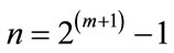
where m is the no. of Level Module used [2].
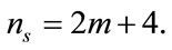
The no. of switches used in the circuit
The input dc voltage fed to kth module varies with particular module no. as:
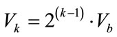
where k = 1, 2, 3 ··· m [3].
The Simulink model of the proposed circuit is shown in Figure 2. In the proposed circuit, 3 Level modules (LM),
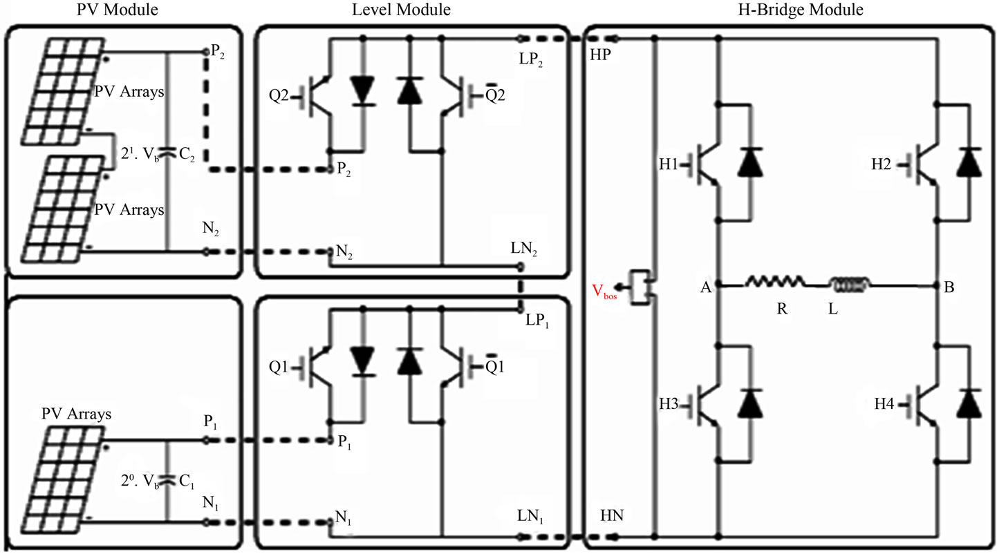
Figure 1. Proposed multilevel circuit of two level module.
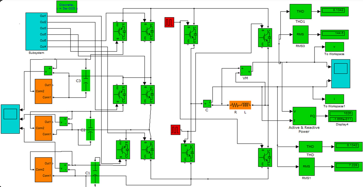
Figure 2. Matlab model for the proposed circuit.
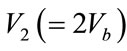
1 H-Bridge inverter, and 3 Solar PV Array of output voltage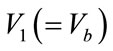 ,
,  and
and 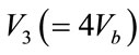 are used. Output wave has 15 levels and the total no. of switches used is 10. Total dc voltage used in the circuit is 7Vb. The gate pulse for first LM switch Q1 is a SPWM pulse having 7 pulses in each half cycle [4]. To find the gate pulse for second LM switch Q2, this Q1 is given to the clock of a negative edge triggered toggle flip flop. Further this Q2 is given to the clock of another toggle flip flop to get gate pulses for third LM switch Q3. The gate pulses for Q1, Q2 and Q3 are shown in Figure 3.
The Simulink Model of PV Array used in the above circuit is shown in Figure 4 [5]. The simulation is done for Vb = 32 Volt. Vb is measured when the PV model is
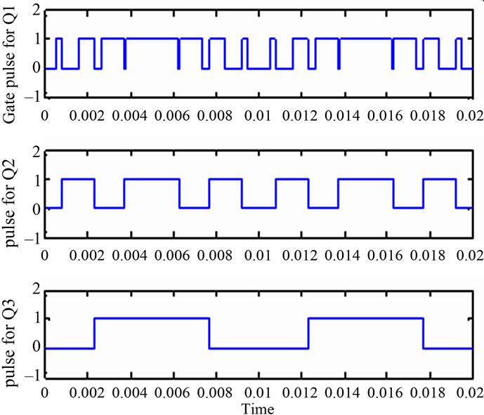
Figure 3. Gate pulses for Q1, Q2 and Q3 respectively.
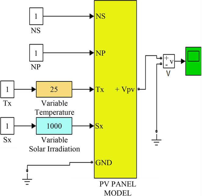
Figure 4. PV Array model used in the proposed circuit.
open circuited. When the PV Array is loaded, some fluctuations in PV Voltage are measured.
When the circuit is simulated, spikes occur in the output voltage wave which tends to deteriorate the power quality. To reduce these spikes, capacitors (C) across PV Array are connected as shown in Figure 2.
3. Simulation and Results
Solar Panel as a dc Source to the Inverter
The proposed circuit is simulated in SIMULINK/MATLAB software.
Panel Output Voltages are , V2 = 64 V and V3 = 128 V, Z = 25 Ω.
Simulation is carried out for an RL load of impedance 25 Ω for different power factor [6]. It is shown that for Pure R (power factor = 1), there is no spike in output voltage wave. But as inductive nature of the load increases, spikes starts and continuously increase which deteriorates the Power Quality. The variation of THD in Load Voltage, RMS Voltage Vr, RMS Current Ir, Active Power P and Reactive Power Q with different load power factor (cosφ) is shown in Table 1.
Table 1 shows that as the power factor decreases from unity, spikes starts appearing and the magnitude of spike increases continuously and hence RMS Voltage increases. Also THD increases which results poor power quality. As the THD increases with the decrement of power factor, THD will become more below 0.8 power factor. Simultaneously Active Power P and Load Current decreases while Reactive power Q increases with the inductive nature of the load.
The spikes obtained in Output Voltage wave for 0.975 and 0.8 power factor is shown in Figures 5 and 6 respectively.
Calculating the Value of Capacitance
Spikes in the Output Voltage are reduced by inserting a
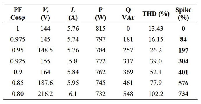
Table 1. Simulation results for proposed multilevel inverter for different power factor without capacitance.
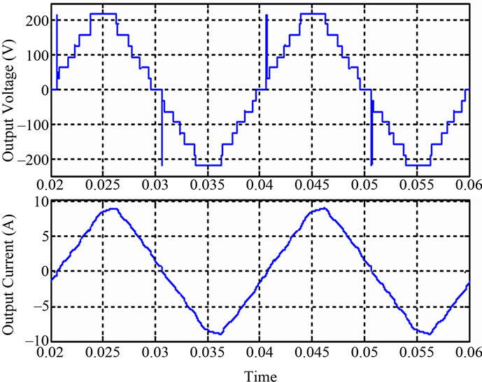
Figure 5. Output voltage and current wave for 0.975 power factor load.

Figure 6. Output voltage and current wave for 0.8 power factor load.
Capacitance across PV Panel. The value of C should be optimum with respect to Cost, Size and power Quality. The variation of THD, Vr, Ir, P and Q with the capacitance value for 0.8 power factor (R = 20 Ω, L = 47.7 mH) is shown in Table 2.
For C = 10 μF
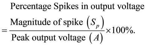
Magnitude of spike = 198 V,
Output Peak voltage = 220 V.
Spike in output voltage
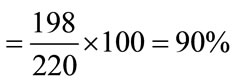 .
.
Table 2 shows that if the value of C increases, spikes decreases and hence RMS Voltage and THD decreases. But the decrement in magnitude of spike and hence in THD becomes very less beyond a certain value of C. So the optimum value with respect to Cost and Power Quality is taken as 50 μF. The voltage and current wave for C = 20 μF is shown in Figure 7.
Finally at C = 50 μF all the parameters are obtained for different value of power factor (keeping load impedance fixed at 25 Ω) as shown in Table 3.
Comparing Tables 1 and 3 it is seen that for same power factor THD reduces up to a great extent after connecting a Capacitor across PV Panel. Load voltage and load current waveforms at C = 50 µF for 0.8 power factor is shown in Figure 8.
It is shown that as the power factor decreases, active power decreases and reactive power increases. Also, the variation of load current Ir with power factor is very small due to the fixed magnitude of impedance Z.
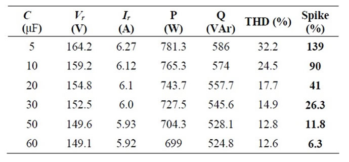
Table 2. Simulation results for proposed multilevel inverter for 0.8 power factor load.
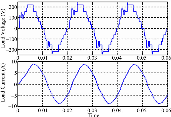
Figure 7. Load voltage and Load current wave at 0.8 power factor and 20 μF capacitance.
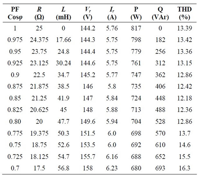
Table 3. Simulation results for proposed multilevel inverter for different power factor with C = 50 µf.
4. Battery as a dc Source to the Inverter
In the proposed circuit, batteries of same voltages are connected in place of Solar Panels. Simulation in SIMULINK/MATLAB software is done for same input dc voltages. Simulation Results are tabulated in Table 4.
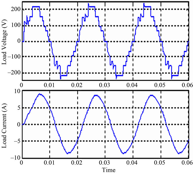
Figure 8. Load voltage and Load current wave at 0.8 power factor and 50 μF capacitance.
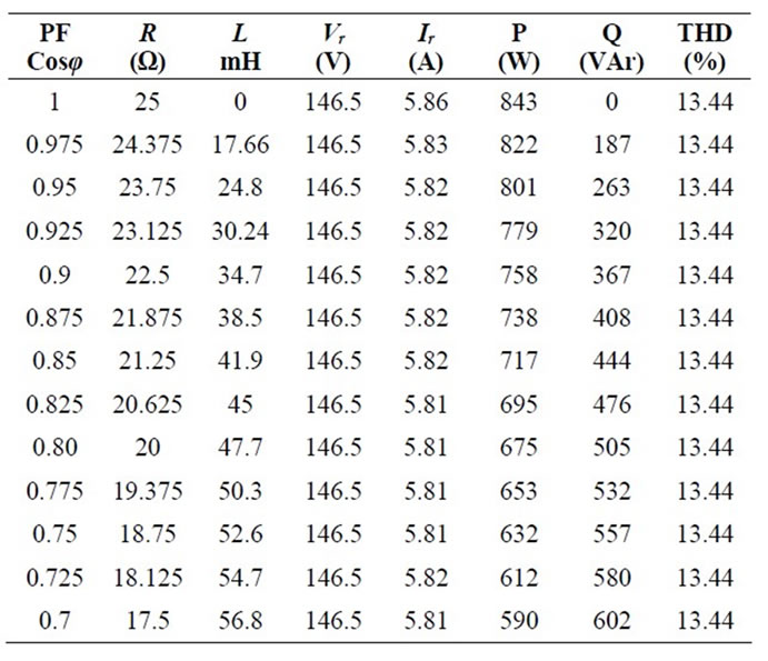
Table 4. Simulation results for proposed multilevel inverter with battery for different power factor.
For Z = 25 Ω,  , V2 = 64 V and V3 = 128 V.
Table 4 shows that for battery as a dc Source, the RMS voltage and THD are constant with the variation of load power factor. Active Power P is maximum at unity power factor while reactive power is zero. When power factor decreases, P decreases and Q increases while the load current is approximately the same (due to fixed Z). Load voltage and current waveforms for inverter with battery as dc source at 0.8 power factor is shown in Figure 9.
5. Comparison
In the proposed topology, for Solar PV as a dc source with capacitance, the THD is decreasing with the load power factor. For unity pf load, THD is 13.39% and for 0.8 PF load THD is 12.86%, i.e. Power Quality becomes better as the load becomes reactive. Below 0.8 PF load, the THD starts increasing. While the circuit having battery as source gives a constant THD of 13.44%. This means that for 0.8 or above power factor load the circuit with PV Panel gives better Power Quality. RMS current rating is approximately same for both the cases. The variation of THD with Load Power Factor for both the cases is shown in Tables 3, 4 and in Figure 10.
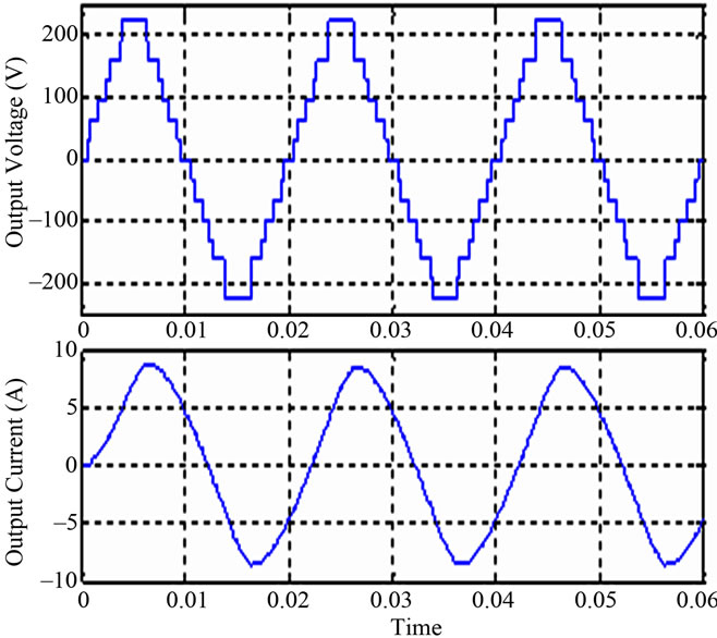
Figure 9. Load voltage and current at 0.8 pf for inverter circuit with battery as source.
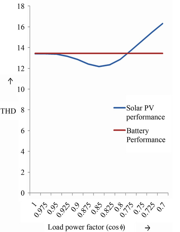
Figure 10. THD vs. load PF graph for proposed circuit with solar panel and battery as dc source.
Comparing the performances above, it is noted that for the power factor of 0.8 or above, the obtained THD is low for solar panel inverter circuit. However, the power obtained is more below 0.85 power factor. As far as active power and passive power as well as power quality are concerned, the solar panel will perform relatively better in the power factor range of 0.8 to 0.85.
6. Conclusions
In this paper, THD in load voltage, Active Power and Reactive Power are evaluated for a proposed inverter circuit with Solar Panel as a dc Source and also a battery using SIMULINK/MATLAB software. The performances are compared for different power factor loads keeping the dc input voltage same without using the filter. In both cases, THD present in load voltage may always be reduced below 5% by the use of filter. The THD obtained from proposed inverter scheme is comparable to THD obtained from conventional inverter scheme but the no. of switches required is less in the proposed scheme.
The overall observation is that in the range of pf from 0.8 to 0.85 the performance of PV panel connected inverter is superior to that with pure dc (battery) as input source.
REFERENCES
- E. Beser, S. Camur, B. Arifoglu and E. Kandemir Beser, “A Grid Connected Photovoltaic Power Conversion System with Single Phase Multilevel Inverter,” Solar Energy, Vol. 84, No. 12, 2010, pp. 2056-2067. doi:10.1016/j.solener.2010.09.011
- E. Kandemir Beser, B. Arifoglu, S. Camur and E. Beser, “Design and Application of a Single Phase Multilevel Inverter Suitable for using as a Voltage Harmonic Source,” Journal of Power Electronics, Vol. 10, No. 2, 2010, pp. 138-145.
- E. Beser, S. Camur, B. Arifoglu and E. Kandemir Beser, “Design and Application of a Novel Structure and Topology for Multilevel Inverter,” 2008 International Symposium on Power Electronics, Electrical Drives, Automation and Motion, Ischia, 11-13 June 2008, pp. 969-974. doi:10.1109/SPEEDHAM.2008.4581249
- M. Ahmad and B. H. Khan, “New Approaches for Harmonic Reduction in Solar Inverter,” IEEE Conference on Students Conference on Engineering and Systems, Allahabad, 16-18 March 2012, pp. 1-6.
- I. H. Altas and A. M. Sharaf, “A Photovoltaic Array Simulation Model for Matlab-Simulink GUI Environment,” International Conference on Clean Electrical Power, Capri, 21-23 May 2007, pp. 341-345.
- http://www.mathworks.com