Energy and Power Engineering
Vol. 4 No. 4 (2012) , Article ID: 20233 , 9 pages DOI:10.4236/epe.2012.44026
A Comparison of Control Methods for Z-Source Inverter
1Department of Control Science and Engineering, Huazhong University of Science and Technology, Wuhan, China
2Electrical & Electronics Engineering Faculty, HCMC University of Transport, Ho Chi Minh City, Vietnam
3HCMC University of Technology, Ho Chi Minh City, Vietnam
Email: phamcongthanh09@yahoo.com
Received May 15, 2012; revised June 18, 2012; accepted June 29, 2012
Keywords: Buck-Boost; Current Source Inverters (CSIs); Pulse-Width Modulation (PWM); Voltage Source Inverters (VSIs); Z-Source Inverters (ZSI)
ABSTRACT
In recent years, Z-source inverters (ZSI) have been proposed as a replacement power conversion concept which it has both voltage buck and boost abilities. In addition, ZSI doesn’t require dead-time to protection short circuit at two switches any of the same phase leg in the inverter bridge and to achieve optimal harmonic of current, voltage. This paper presents two different control methods (CM) for ZSI. The aim of this study to compare between two modulation methods, there are modified space vector pulse width modulation method (MSVM) and the simple boost control (SBC) about the unique harmonic performance features, the total average and peak switching device power of the inverter system. In addition, this paper also analyzes about the ability exceed modulation index in linear region of two CM using MATLAB/Simulink.
1. Introduction
In a conventional voltage source inverter, the two switches of any phase leg cannot be gated at the same time because this may cause a short circuit situation and thus destroy the inverter. In addition, the maximum output voltage cannot exceed the dc bus voltage. These limitations in such conventional voltage source inverter can be overcome by using ZSI [1], Figure 1.
A comparison among conventional pulse-width modulation (PWM) inverter, dc-dc boosted PWM inverter and ZSI but ZSI shows that higher efficiency and lower cost. Because of these reasons, ZSI has applied in hybrid electric vehicles [2,3]. In addition, in [4] show comparison among the traditional I-source inverter and (VSI) with the Z-source network should require less capacitance, inductance and size smaller than traditional dc-dc boosted PWM inverter. Therefore, these results in increasing attention on ZSI, especially for the application where the dc input source has a wide voltage variation range such as fuel cell, battery, lead acid. Also, the ZSI has applied for direct-drive wind generation system and photovoltaic power system base on tracking algorithm maximum power and hybrid electric vehicles [5-7].
Additionally, the maximum boost control is alike the conventional carrier-based PWM method base on all zero voltage vectors, shoot through state (the other zero vectors) and the six active states which are maintained unchanged but the main drawbacks of this modulation method is big inductor ripple and a large inductor when the output frequency is low. Therefor, they will increase the cost and size of the circuit [8].
Given its many benefits, many studies have been researched into CM of ZSI. Cosequently, how chose CM which highest efficiency is very important in control systems of ZSI. Through detailed analysis, the aim of this study to show how various two CM for ZSI, there are MSVM and the SBC which they are analyzed and compared about the unique harmonic features of current, voltage and the total average switching device power, the total peak switching device power of the inverter system. In addition, this paper also analyzes about the ability exceed modulation index in linear region of two CM using simulation MATLAB/Simulink.
2. Equivalent Circuit, Operating Principle and Total Switching Device Power of ZSI
2.1. Equivalent Circuit, Operating Principle of ZSI
In Figure 1 show ZSI voltage-type configuration, which include inductors (L1 and L2) are similar inductance L,
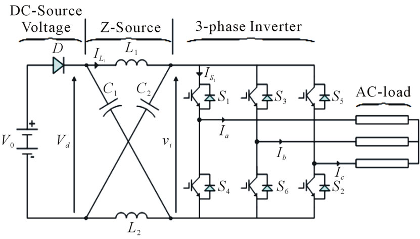
Figure 1. ZSI voltage-type configuration.
simultaneously capacitors (C1 and C2) are similar capacitance C. Where L and C are connected in X shape, the dc input voltage source which may be fuel cell, battery or diode rectifier. The general inverter have two zero voltage vector and six active voltage vectors but in the threephase ZSI has one additional zero voltage vector that is third zero state vector or the shoot-through zero state. The influence of this phase-leg shoot-through on the inverter performance can be considered the equivalent circuits shown in Figure 2. In operating principle of ZSI there are two operating modes: non-shoot-through mode and shoot-through mode. In non-shoot-through mode Figure 2(a) that the ZSI operates under the conventional PWM. The shoot-through state is forbidden in the conventional inverter but in the ZSI the shoot-through mode are given in Figure 2(b). In Figure 2(b) show that the load terminals of any phase legs are shorted both the upper and lower. At that time, the dc capacitor voltage can be boosted to the desired value.
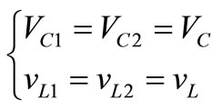
Where β is the angle between the reference voltage vector  and voltage vector V1. Because assume inductors (L1 and L2), capacitors (C1 and C2) have alike inductance (L) and capacitance (C) respectively, we have
 (1)
(1)
• Non shoot-through time internal of one period non shoot-through zero state for a period  in Figure 2(a), we have:
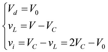 (2)
(2)
• Shoot-through time internal of one period shootthrough zero state for a period  in Figure 2(b), we have:
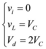 (3)
(3)
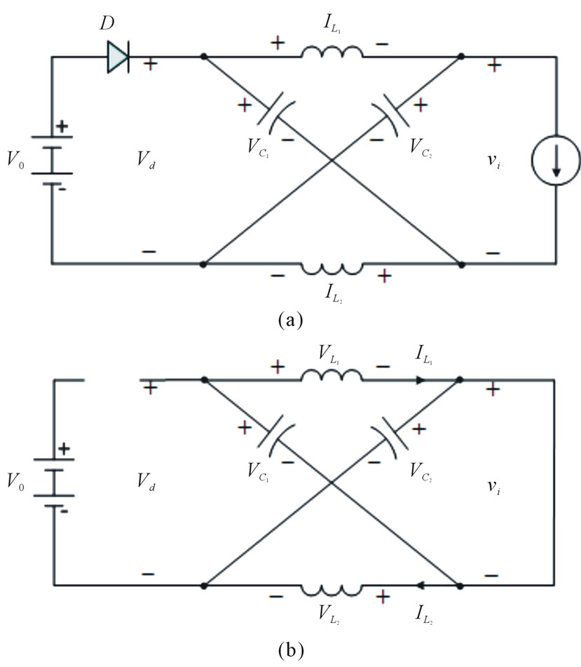
Figure 2. Equivalent circuits of ZSI. (a) Non-shoot-through mode; (b) Shoot-through mode.
where  is the dc source voltage and one period switching cycle Tsf, where
 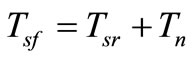 and
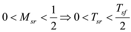
and  is the shoot-through time duty ratio.
The average voltage of the inductors over one switching period should be zero in steady state, from (2) and (3) thus capacitor voltage can expressed:
 (4)
(4)
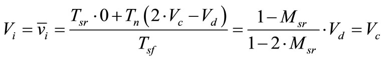 (5)
(5)
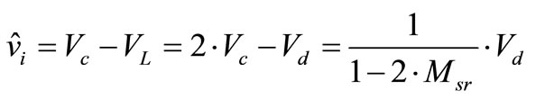 (6)
(6)
 (7)
(7)
From (6), if  is increase then
  is also increase, where
  is the voltage stress across switching devices.
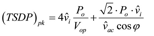
2.2. Total Switching Device Power (TSDP)
In an inverter system, choice switching device must depend on the peak, average current and the maximum voltage impressed going through it. The switching device power is introduced to quantify the voltage and current stress of an inverter system [8]. TSDP is a measure of the total semiconductor device requirement.
The total average switching device power of the inverter system  is given in [8]:
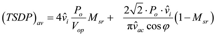 (8)
(8)
The total peak switching device power of the inverter system  is also given in [8]:
 (9)
(9)
where N is the number of switching devices used,  the inductor current,
  the output peak phase voltage from the inverter and Po maximum power output of the DC-source voltage.
3. Proposed CM of MSVM and SBC
3.1. Proposed CM of MSVM
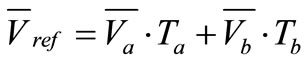
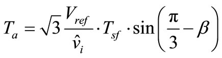
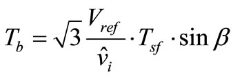
Nowadays, the space vector PWM (SVM) method have widely used at regulated PWM inverter due to a higher modulation index and lower current harmonics in [9]. The SVM is suitable to control the shoot-through time in ZSI. Where V0, V7 and shoot-through are zero vectors (in ZSI), where V1 to V6 are the six active vectors. If the reference voltage vector  (the sinusoidal three-phase command voltage of output ZSI with minimum amount of harmonic distortion) is located between the arbitrary vector Va and Vb, the reference voltage vector is divided into the two adjacent voltage vectors (Va, Vb) and zero vectors (V0, V7 and shoot-through) in Figure 3. When
  rotate around section (1 - 6) of hexagon while (a, b) are changed: (a, b) = (1, 2); (2, 3); (3, 4); (4, 5); (5, 6) in every sector, respectively. In one sampling interval, Va and Vb are applied at times Ta and Tb, respectively, and the zero vector is applied at time
 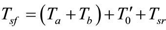 where
where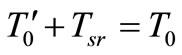 .
.
Consequently, from (10), the reference voltage vector  can be given by
 (10)
(10)
 (11)
(11)
 (12)
(12)
The conventional SVM in Figure 4(a) and the MSVM in Figure 4(b) where  is shoot-through time has an extra for boosting the dc link voltage of the inverter beside time intervals Ta, Tb and T0.
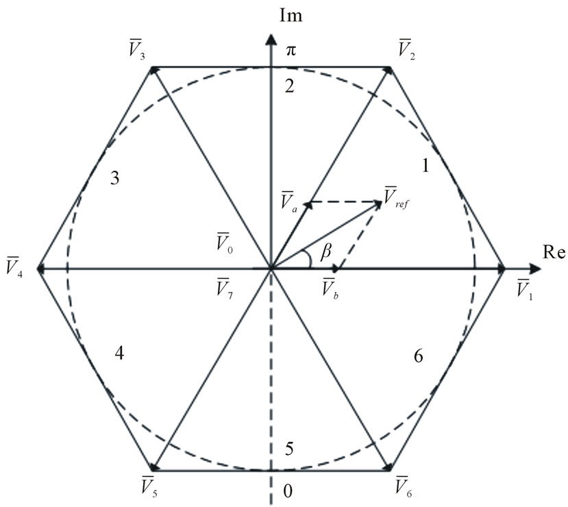
Figure 3. Voltage vector through conven-tional SVM of VSI.
From Figure 4 the shoot-through states (STS) are evenly assigned to each phase with 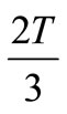 within zero voltage period
  and
and  within active voltage period
  and
and  within active voltage period
 , where Ta and Tb are unchanged. So the STS does not affect the SVM CM of the inverter, and it is limited to the zero state time T0. Where T are determined by (13). Therefore, the STS should be inserted period intervals are maintained at the start and end of the switching cycle to achieve alike optimal harmonic performance.
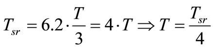 (13)
(13)
From (7) we have
 (14)
(14)
In the undermodulation region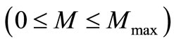 .
.
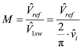
Figure 3, Vref always remains within hexagon in [10]. Let us define a modified modulation factor M given by
 (15)
(15)
where  = vector magnitude (or phase peak value), in the linear region
  is the output peak phase voltage from the inverter
  and
and  = fundamental peak value
  of the square-phase voltage
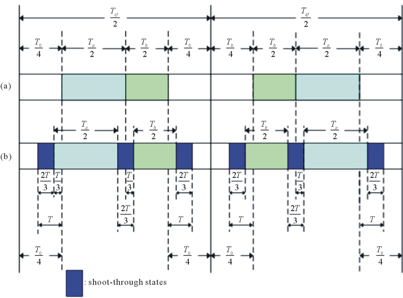
Figure 4. MSVM (a) Switching patterns for traditional SVM; (b) Switching patterns for MSVM.
wave. The maximum possible value of modulation factor  at the end of the under modulation region can derived. The radius
  Figure 3 of the inscribed circle can be given as
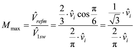 (16)
(16)
This means that 90.7 percent of the fundamental at the square wave is available in the linear region.
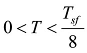
3.2. The Simple Boost Control (SBC)
The SBC method strategy inserts STS in all the PWM conventional zero states during one switching period. The six active states are maintained unchanged as in the conventional carrier based PWM [2]. When the triangular waveform is greater than the upper envelope,  , or lower than the bottom envelope,
  , the circuit turns into shoot-through state, show Figure 5. The output peak phase voltage from the inverter can be given by
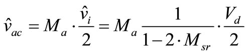 (17)
(17)
where  is the modulation index of magnitude
 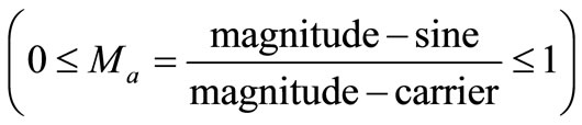 in [10]. At
 M = modulation factor, in the linear region (0 ≤ M ≤ Mmax)
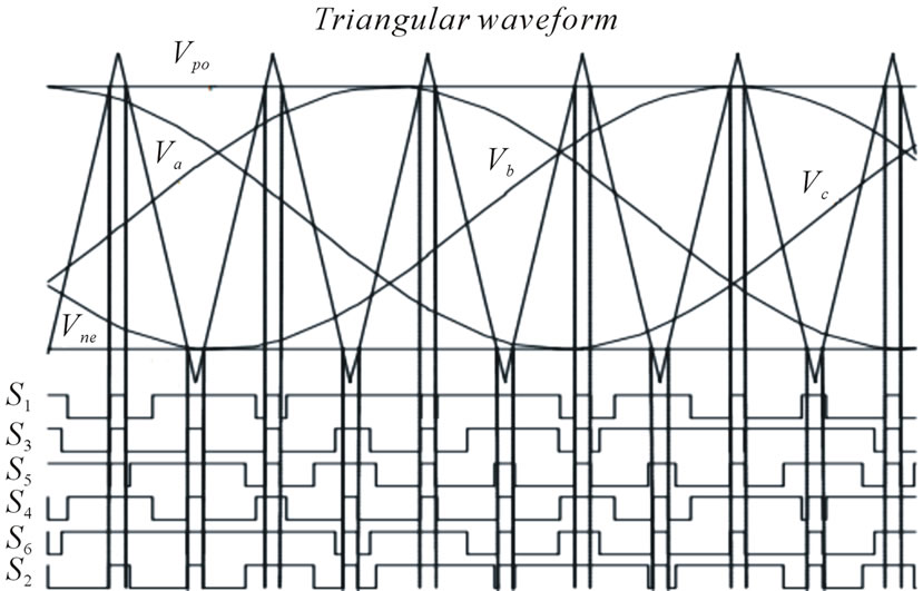
Figure 5. Simple boost control.
where Mmax = maximum modulation factor determined by
 (18)
(18)
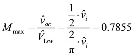
At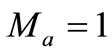 , the maximum value of fundamental peak voltage is
 , Which is 78.55 percent of peak voltage
 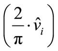 of the square wave. From (16), (18) we can see that the maximum value of fundamental peak voltage of the MSVM method is higher than the SBC method. Therefore, the MSVM method modulation index in linear can exceed more than the SBC method.
4. Simulation
To verify the validity of the above analysis, simulation models shown in Figure 1 use Matlab/Simulink for MSVM and SBC methods of z-source inverter are analyzed. The simulation for two CMs with parameters are the same, see Table 1.
In Figure 6 shows the inverter’s dc link voltage, the ZSI’s capacitor voltage and comparison with maximum output voltage of DC-source. We observe from the figure that the inverter’s dc link voltage  boosted to (500 V) greater than maximum output voltage of DC-source (400 V) is (100 V) see Table 2.
In Figure 7 shows the switching output line voltage and phases voltage waveform of ZSI with MSVM methods. Figures 8 and 9 show output line voltage and current sine waveforms of ZSI with MSVM and SBC methods, respectively.
Output line peak voltage and peak current sine waveforms of ZSI with MSVM method greater than output line peak voltage and peak current sine waveforms of ZSI with SBC method, respectively.
Figures 10 and 11 show total harmonic disturbance spectra of output line voltage 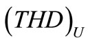 and total harmonic disturbance spectra of output current
  which
which  and
and  of MSVM method less than
  and
and  of SBC method. These results are given in Table 2. Also in Table 2 show calculate results of MSVM and SBC methods use Equations (4)-(18).
 ,
,  of MSVM method less than
 ,
,  of SBC method.
In the future, we will apply MSVM for ZSI in many control systems (e.g. motor speed control system, hybrid electric vehicles, photovoltaic, direct-drive wind generation system). In Figure 12 shows the figure experiments for motor speed control system.
5. Acknowledgements
I am extremely grateful to professors’ lecture speeches during the course at Department of Control Science and Engineering, Huazhong University of Science and Techno-
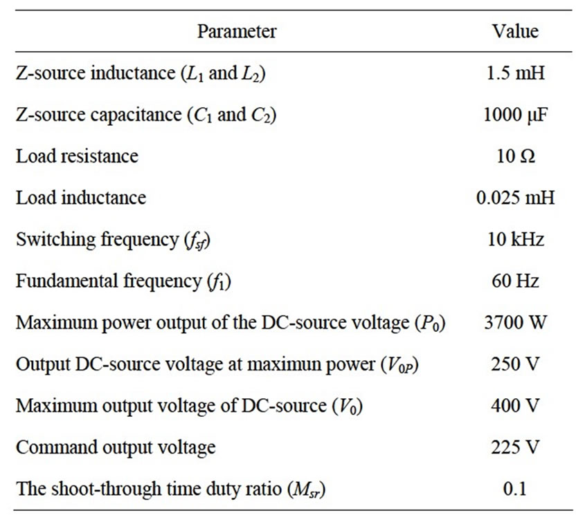
Table 1. Parameters are used for simulation of MSVM and SBC.
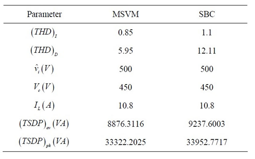
Table 2. Calculate results of MSVM and SBC.
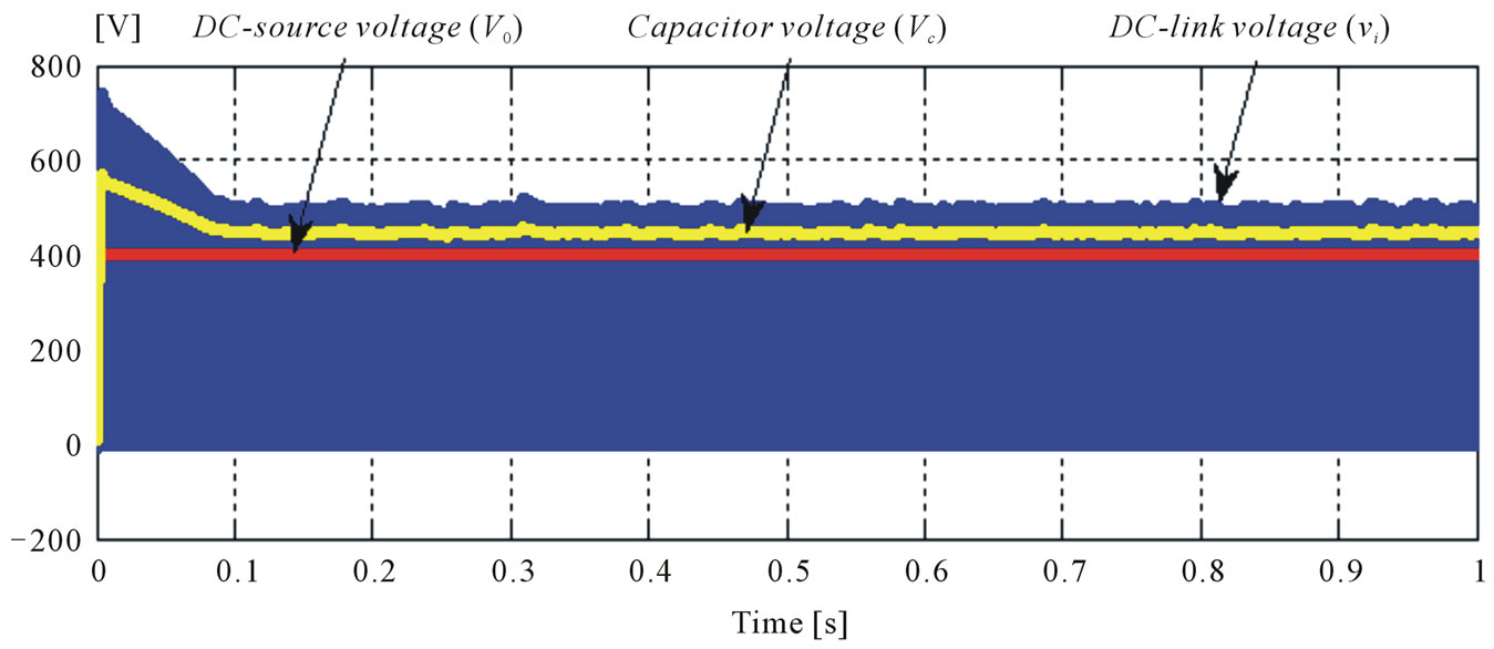
Figure 6. Simulation MSVM. DC-link voltage (vi), Capacitor voltage (Vc) and DC-source voltage (V0).
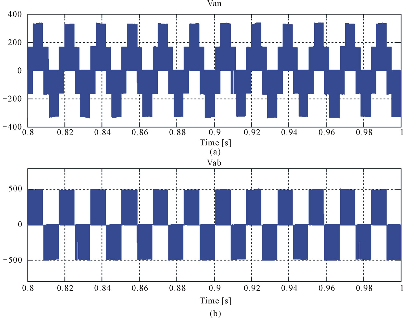
Figure 7. Switching output line voltage and phases voltage waveform of ZSI (MSVM). (a) Switching output phase voltage; (b) Switching output line voltage.
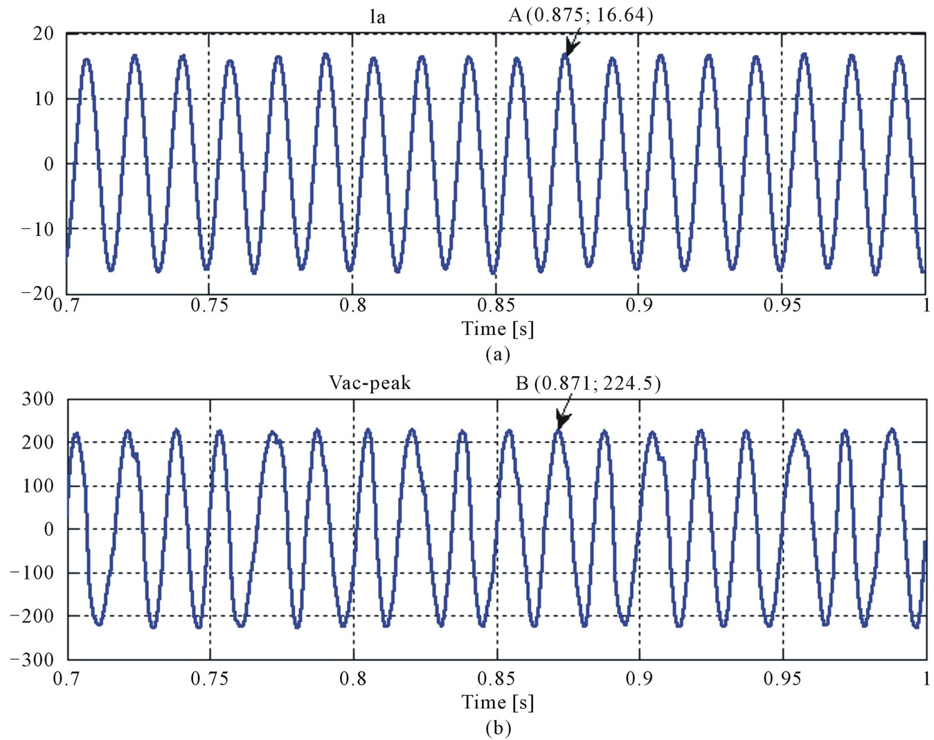
Figure 8. Output line voltage and current sine wave-forms of ZSI (MSVM). (a) Output current sine wave-forms; (b) Output line voltage sine waveforms.
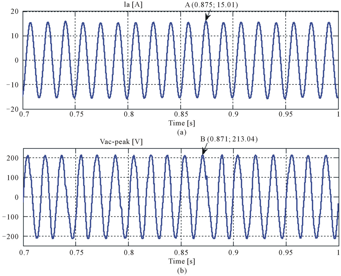
Figure 9. Output line voltage and current wave-forms of ZSI (SBC). (a) Output current; (b) Output line voltage.
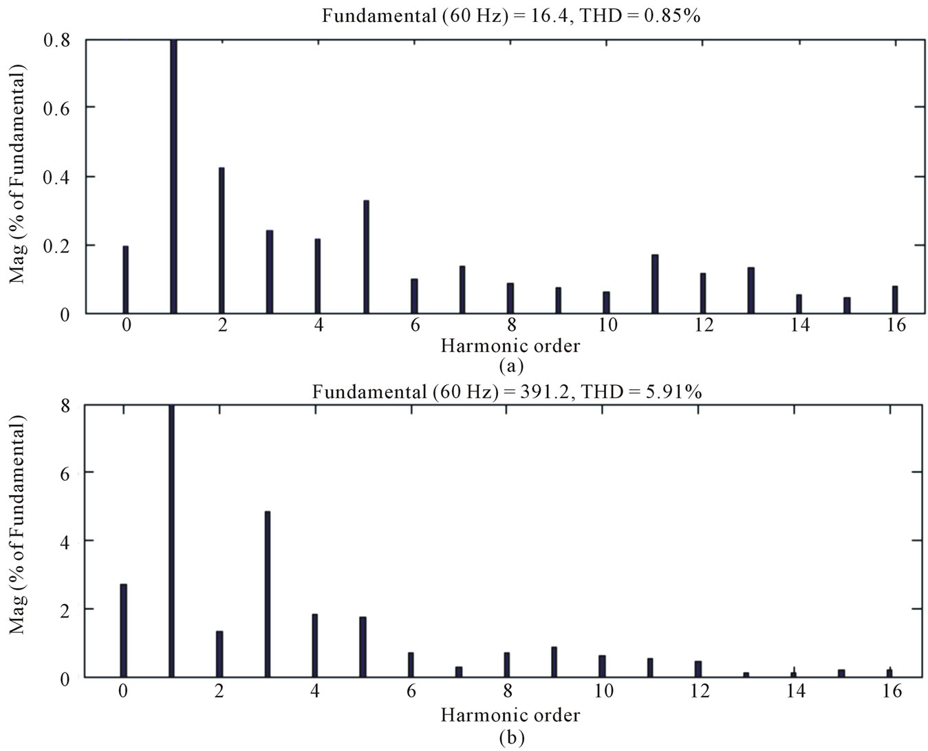
Figure 10. Harmonic spectra of Z-source inverter (MSVM). (a) Harmonic spectra of output current; (b) Harmonic spectra of output line voltage.

Figure 11. Harmonic spectra of Z-source inverter (SBC). (a) Harmonic spectra of output current; (b) Harmonic spectra of output line voltage.
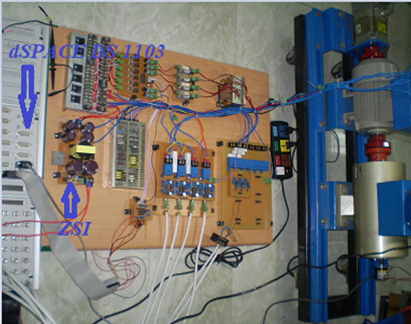
Figure 12. The figure experiments for motor speed control system.
logy (HUST), Wuhan 430074, China. Especially, professor Anwen Shen, associate professor Phan Quoc Dzung, and master Nguyen Bao Anh who offers me advice and help me to finish this paper.
6. Conclusion
This paper presents a comparison of two different MM there are MSVM and the SBC for ZSI. They show the harmonic spectra of output voltage and output current with MSVM is less than harmonic spectra of output voltage and output current with SBC, the total average and peak switching device power of ZSI system with MSVM method is less than the total average and peak switching device power of ZSI system with SBC, the MSVM modulation index in linear can exceed more than the SBC. All of these comparisons are used simulation MATLAB/Simulink.
REFERENCES
- I. P. C. Loh, D. M. Vilathgamuwa, I. Senior, Y. S. Lai, G. T. Chua and I. Y. W. Li, “Pulse-Width Modulation of Z-Source Inverters,” IEEE Transactions on Power Electronics, Vol. 20, No. 6, 2005, pp. 1346-1355. doi:10.1109/TPEL.2005.857543
- M. Olzwesky, “Z-Source Inverter for Fuel Cell Vehicles,” US Department of Energy, Freedom CAR and Vehicles Technologies, EE-2G, Washington, 2005.
- K. Holland, M. Shen and F. Z. Peng, “Z-Source Inverter Control for Traction Drive of Fuel Cell-Battery Hybrid Vehicles,” Industry Applications Conference, 40th IAS Annual Meeting, Vol. 3, No. 4, 2005, pp. 1651-1656.
- I. Fang and Z. Peng, “Z-Source Inverter,” IEEE Transactions Industry Applications, Vol. 39, No. 2, 2003, pp. 990-997.
- J. Li, K. Q. Qu, X. L. Song and G. C. Chen, “Study on Control Methods of Direct-Drive Wind Generation System Based on Three-Phase Z-Source Inverter,” IPEMC, Shanghai, 17-20 May 2009.
- S. A. K. H. Mozafari Niapoor, S. Danyali and M. Sharifian, “Photovoltaic Power System Based mppt Z-Source Inverter to Supply a Sensorless BLDC Motor,” 1st Power Electronic, Drive Systems and Technologies Conference, University of Tabriz, Tabriz, 17-18 February 2010.
- U. Ali and V. Kamaraj, “A Novel Space Vector pwm for Z-Source Inverter,” Proceedings of ICETECT, Nagercoil, 23-24 March 2011.
- M. Shen, A. Joseph, J. Wang, F. Z. Peng and D. J. Adams, “Comparison of Traditional Inverters and Z-Source Inverter for Fuel Cell Vehicles,” IEEE Power Electronics Society, Vol. 22, No. 4, 2007, pp. 1453-1500. doi:10.1109/TPEL.2007.900505
- T. Chun, Q. Tran, J. Ahn and J. Lai, “Ac Output Voltage Control with Minimization of Voltage Stress across Devices in the Z-Source Inverter Using Modified svpwm,” PESC 37th IEEE, Jeju, 18-22 June 2006, pp. 1-5.
- B. K. Bose, “Modern Power Electronics and AC Drivers,” Pearson Education, Upper Saddle River, 2002.