World Journal of Condensed Matter Physics
Vol.3 No.4(2013), Article ID:37903,5 pages DOI:10.4236/wjcmp.2013.34026
Influence of Iodine Pressure on the Growth of CuIn1−xGaxSe2 Thin Films Obtained by Close-Spaced Vapor Transport “CSVT”
![]()
1Department of Physics, Faculty of Sciences II, Lebanese University, Jdeidet, Lebanon; 2Centre Electronique et Micro-Opto- électronique de Montpellier (CEM2), Faculté Sciences et Techniques du Languedoc, Université de Montpellier II, Montpellier, France.
Email: dayane_habib@yahoo.fr
Copyright © 2013 Dayane Habib et al. This is an open access article distributed under the Creative Commons Attribution License, which permits unrestricted use, distribution, and reproduction in any medium, provided the original work is properly cited.
Received July 24th, 2013; revised September 6th, 2013; accepted September 21st, 2013
Keywords: Chemical Vapor Deposition; CuIn1−xGaxSe2; Thin Films; Chalcopyrite; Photovoltaic
ABSTRACT
We present the results concerning photovoltaic materials CuIn1−xGaxSe2 thin films, which were obtained by closespaced vapor transport “CSVT”. The influence of the iodine pressure on the growth of CuIn1−xGaxSe2 thin films was studied. The thin films were characterized by Energy Dispersive Spectrometry (EDS), Scanning Electron Microscope (SEM), hot point probe method, X-Ray Diffraction (XRD), Photoluminescence, and Optical response (Photoconductivity). At high pressure, the deposition rate was very important. The films were relatively thick and homogeneous with large grains dimensions. These films are formed of crystals placed in a preferential orientation depending on the plan (112). At low pressure, the films were thin and inhomogeneous with relatively small grains. These films of crystals didn’t have preferential orientation.
1. Introduction
Chalcopyrite semiconductors CuInSe2, CuGaSe2 and their solid solution are well known as promising candidates for the fabrication of thin film heterojunctions for photovoltaic application. A conversion efficiency of 20% was reported for solar cells based on Cu(In,Ga)Se2 [1]. Several processes are available for commercial application: Flash Evaporation [2], MOCVD [3], Electrodeposition [4], rf Sputtering [5], Coevaporation [6], Spray Pyrolysis [7], Selenization [8], rapid thermal processing (RTP) [9] or Close-Spaced Vapor Transport “CSVT”.
In this paper, we study the influence of the iodine pressure on the growth of CuIn1−xGaxSe2 thin films obtained by the “CSVT” method. Energy Dispersive Spectrometry (EDS) and X-ray Diffraction (XRD) were used to calculate the compositions and lattice parameters of the films. Scanning Electron Microscope (SEM) enabled us to check their quality (grains size and morphology). Photoluminescence and photoconductivity allowed us to check their optical properties.
2. Experiment
The “CSVT” method needs a very simple and inexpensive reactor (Figure 1) described in [10]. It consists of a vertical quartz tube, with an inner diameter of about 20 mm, and a length of 10 - 20 cm, attached to a vacuum system. At the bottom of this reactor, there was a silice support on which the CuIn1−xGaxSe2 source (chip with a thickness e = 1 mm prepared from grains powder < 5 µm under a pressure of 5 × 10³ kg/cm2) [11] is putted. A soda lime glass substrate plate was set above the source at a close distance (0.5 mm < d < 3 mm), by means of a ring spacer of quartz glass. The transport reagent, composed of iodine grains, was located at the upper part of the substrate. The complete system was installed on an external SiC rod. The source temperature depends on the electric voltage applied to this SiC heating element, the quartz plate thickness of ring spacer, and the distance d’ between the reactor and the heating element. The substrate temperature is a function of the source temperature, the distance d between the source and the substrate, and the
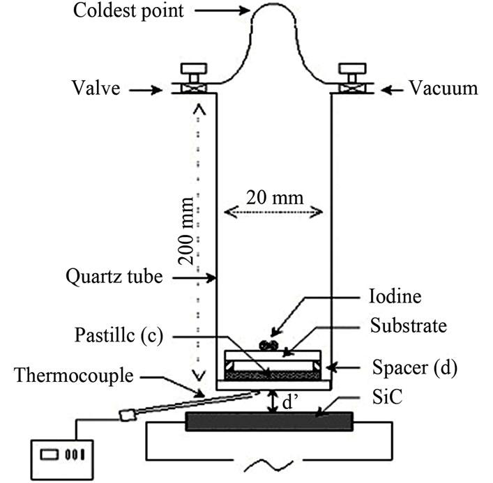
Figure 1. Schematic diagram of the “CSVT” reactor.
gases pressure inside the reactor.
The reaction begins when iodine vaporizes and invades the tube; the pressure of the iodine was determined by the temperature (tcp) of the coldest point in the tube [11], generally at the level of the top.
The iodine vapor pressure (PI2) (Figure 2) was calculated from the following equation:
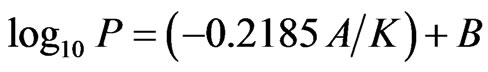 (1)
(1)
where P is the pressure expressed in Torrs, K is the temperature in Kelvin, and A is the molar heat of vaporization in calories per gram mole (A = 13056.6 and B = 9.237273).
Iodine decomposes and reacts with the chip surface by etching. The gaseous elements are transported to the substrate, slightly colder than the source (about 50˚C to 100˚C). These elements settle and reconstitute the material.
3. Results and Discussion
Two series of CuIn1−xGaxSe2 (0 ≤ x ≤ 1) compound thin films corresponding to two values of the iodine pressure were studied. The vapor iodine pressure is varied by varying the temperature (tcp) of the coldest point in the tube (30˚C corresponding to PI2 = 0.66 Torrs and 70˚C to 8.31 Torrs) (Figure 2). At low iodine pressure (tcp = 30˚C, PI2 = 0.66 Torrs), the films obtained are thin (Table 1) and inhomogeneous. Two different zones were observed. The first is at the center, formed by melted selenium and crystals. The second, is the area around the center formed by well oriented crystals following a several preferential directions ((112), (220), (204), (316), (116)) indicated by X-ray spectra (Figure 3(a)).
At high pressure (PI2 = 8.31 Torrs) corresponding to tcp = 70˚C, thick films (Table 1) were obtained during a shorter time of transport compared to the low pressure case. These films were homogeneous and formed by well oriented crystals following the direction (112) (Figure 3(b)).
In both cases, the size of crystals increases with the proportion of gallium. The lattice parameters a and c vary only linearly with x (Figure 4). These values decrease as the gallium concentration increases [12-14], since the gallium atom is much smaller than that of Indium. In all cases, c/a ratio is found to be nearly 2.
The analysis of the chemical composition by EDS (Figure 5) shows the presence of a small quantity of
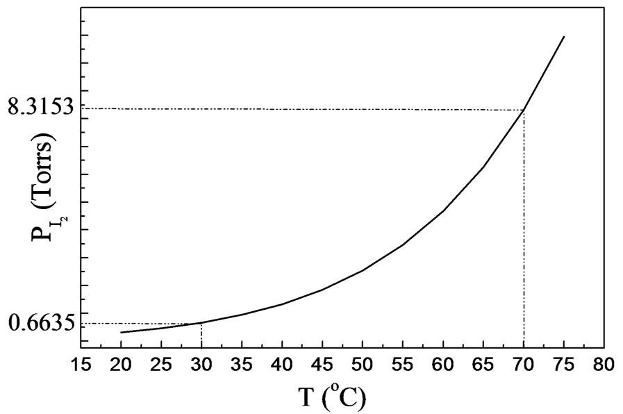
Figure 2. The iodine vapor pressure (PI2) is shown as a function of the temperature. This curve was calculated using Equation (1).
 (a)
(a)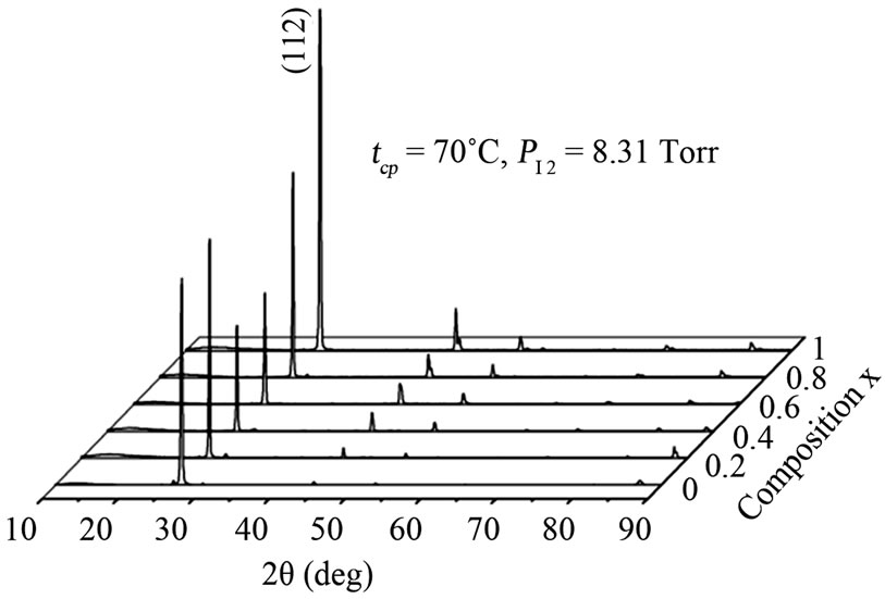 (b)
(b)
Figure 3. X-ray diffraction patterns of CuIn1−xGaxSe2: (a) tcp = 30˚C, PI2 = 0.66 Torr; (b) tcp = 70˚C, PI2 = 8.31 Torr.
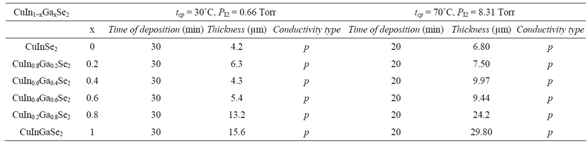
Table 1. Thickness, conductivity type and deposition time of different CuIn1−xGaxSe2 samples.
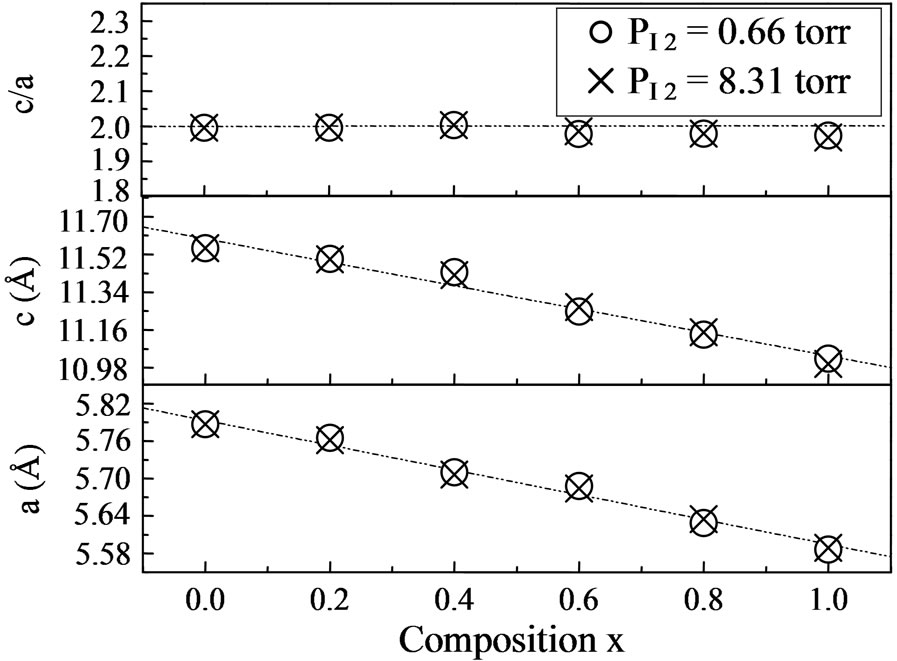
Figure 4. Lattice parameters (a and c) for CuInxGa1−xSe2: (š) tcp = 30˚C, PI2 = 0.66 Torr and (Ï) tcp = 70˚C, PI2 = 8.31 Torr.
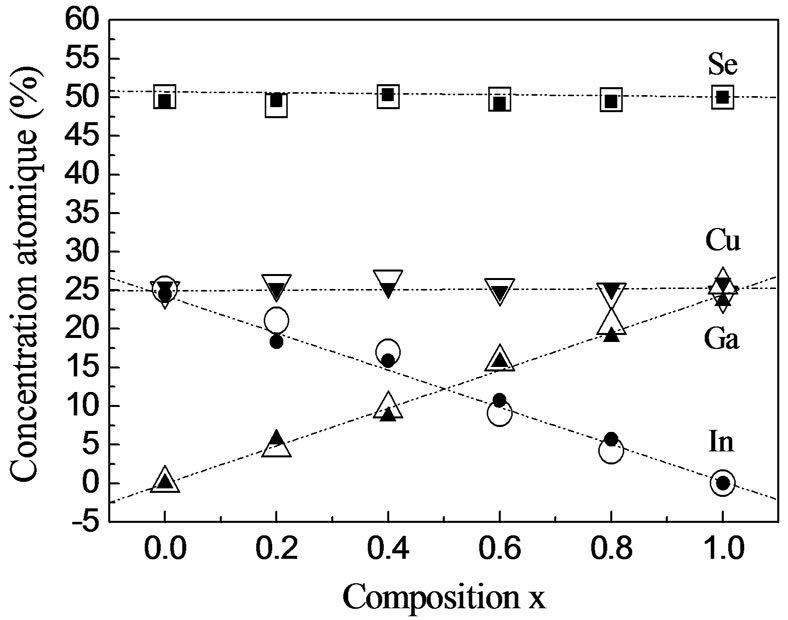
Figure 5. Composition of CuInxGa1−xSe2 thin films determined by EDS as a function of the source composition x: ▼Cu, ●In, ▲Ga, ■ Se (tcp = 30˚C, PI2 = 0.66 Torr), and  Cu, ○ In,
  Ga, □ Se (tcp = 70˚C, PI2 = 8.31 Torr).
iodine in the films prepared at high PI2, whereas iodine is not detected in those grown at low pressure. Iodine may be removed by annealing at 100˚C. Figure 6 shows the morphologies of the surface, showing that the sizes of crystals prepared at high PI2 are bigger (10 µm < Φ < 25 µm). The crystals have a better orientation than those grown at low PI2 (3 µm < Φ < 10 µm). This result shows
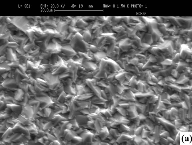

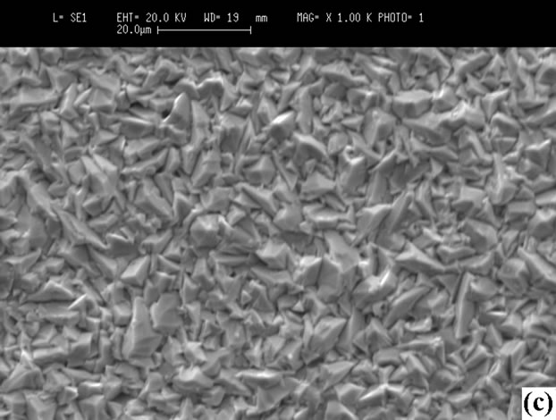
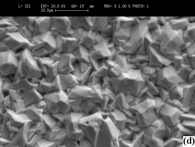
Figure 6. Surfaces SEM micrographs of the films: (a) CuInSe2; (b) CuGaSe2 (tcp = 30˚C, PI2 = 0.66 Torr); (c) CuInSe2; (d) CuGaSe2 (tcp = 70˚C, PI2 = 8.31 Torr).
that the growth with a high iodine pressure is better.
Figures 7(a) and (c) show the spectra of Photoluminescence at liquid Helium temperature (4.2 K) of the alloy CuIn1−xGaxSe2 thin films (x = 0 and x = 1) prepared at high PI2. An increase in the gap value of the materials CuIn1−xGaxSe2 as a function of the concentration of Ga was observed. The band gap energy value at room temperature is determined in analyzing our compounds by spectral Photoconductivity [15]. Figures 7(b) and (d)
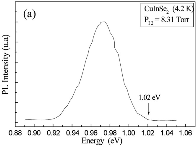
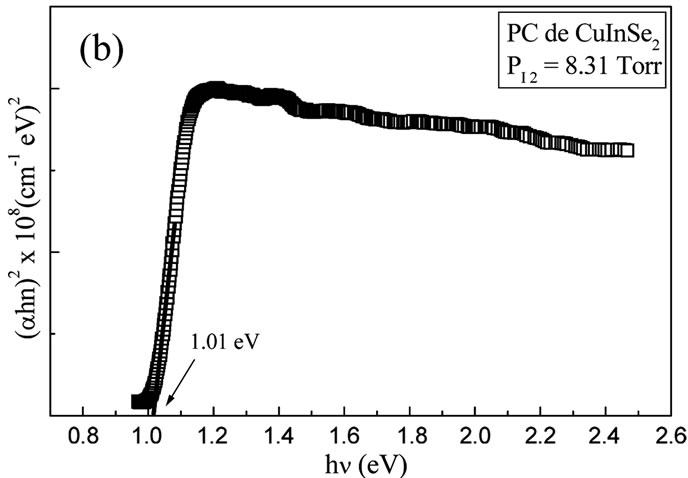
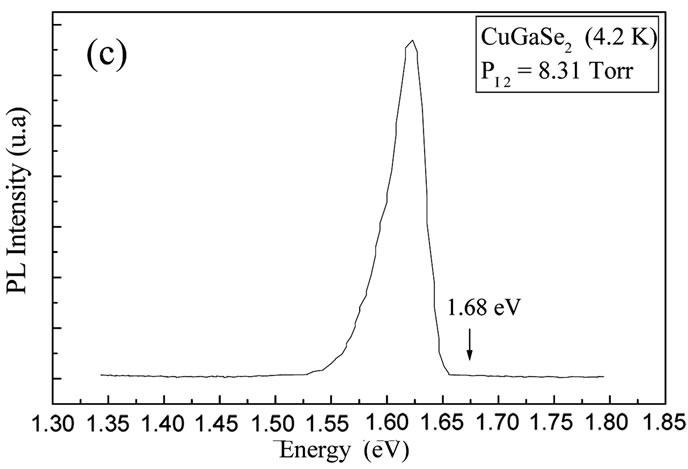

Figure 7. ((a), (c)) Variation of PL dominant peak of CuIn1−xGaxSe2 thin films (x = 0 and x = 1) prepared at high PI2; (b, d) The spectra of Photoconductivity ((αhν)2 as a function of (hν) of the CuIn1−xGaxSe2 thin films (x = 0 and x = 1) prepared at high PI2.
illustrate the spectra of Photoconductivity ((αhν)2 as a function of hν) of the CuIn1−xGaxSe2 thin films (x = 0 and x = 1) prepared at high PI2. These values are in good agreement with those found by Photoluminescence and in literature [15-17].
The band gap of the thin films which prepared at low iodine pressure (tcp = 30˚C, PI2 = 0.66 Torrs) could not be observed, caused probably by the present of the melted selenium, or the thin films prepared at these low pressure are not brilliant.
4. Conclusion
CuIn1−xGaxSe2 thin films at two different iodine pressures were studied. At high pressure, the deposition rate is very important. The films are relatively thick and homogeneous with large grains dimensions. These films are formed of crystals placed in a preferential orientation depending on the plan (112). At low pressure, the films are thin and inhomogeneous with relatively small grains. These films of crystals didn’t have preferential orientation. The characterization by Photoluminescence and Photoconductivity allows us to determinate the band gap values of the thin films prepared at high PI2 which vary from 1.02 eV to 1.68 eV. The band gap of the thin films prepared at low PI2 is not observed, probably due to the present of the melted selenium, or the no brilliant thin films prepared at this low pressure.
REFERENCES
- I. Repins, M. A. Contreras, B. Egaas, C. DeHart, J. Scharf, C. L. Perkins, B. To and R. Noufi, “New World Record Efficiency for Cu(In,Ga)Se2. Thin-Film Solar Cells beyond 20%,” Progress in Photovoltaics: Research and Applications, Vol. 16, No. 3, 2008, pp. 235-239. http://dx.doi.org/10.1002/pip.822
- H. Sakata and N. Nakao, “Optical and Electrical Properties of Flash-Evaporated Amorphous CuInSe2 Films,” Solar Energy Materials and Solar Cells, Vol. 63, No. 3, 2000, pp. 259-265. http://dx.doi.org/10.1016/S0927-0248(00)00032-5
- G. Orsal, N. Romain, M. C. Artaud and S. Duchemin, “Characterization of CuGaSe2 Thin Films Grown by MOCV,” IEEE Transaction on Electron Device, Vol. 46, No. 10, 1999, pp. 2098-2102. http://dx.doi.org/10.1109/16.792003
- S. Nakamura, S. Sugawara, A. Hashimoto and A. Yamamoto, “Influence of Annealing Temperature on the Properties of Cu(In,Ga)Se2. Thin Films by Thermal Crystallization in Se Vapor,” Solar Energy Materials & Solar Cells, Vol. 50, No. 1-4, 1998, pp. 25-30. http://dx.doi.org/10.1016/S0927-0248(97)00097-4
- I. Martil, J. Santamaria, G. Gonzalez Diaz and F. Sanchez Quesada, “Structural, Electrical, and Optical Properties of CuGaSe2 rf Sputtered Thin Films,” Journal of Applied Physics, Vol. 68, No. 1, 1990, pp. 189-193. http://dx.doi.org/10.1063/1.347113
- S. H. Kwon, B. T. Ahn, S. K. Kim, K. H. Yoon and J. Song, “Growth of CuIn3Se5 Layer on CuInSe2 Films and Its Effect on the Photovoltaic Properties of In2Se3/ CuInSe2 Solar Cells,” Thin Solid Films, Vol. 323, No. 1-2, 1998, pp. 265-269. http://dx.doi.org/10.1016/S0040-6090(97)00928-0
- K. T. Ramakrishna Reddy and R. B. V. Chalapathy, “Preparation and Properties of Sprayed CuGa0.5In0.5Se2 Thin Films,” Solar Energy Materials & Solar Cells, Vol. 50, No. 1-4, 1998, pp. 19-24. http://dx.doi.org/10.1016/S0927-0248(97)00096-2
- J. H. Schon, V. Alberts and E. Burcher, “Sharp Optical Emissions from Cu-Rich, Polycrystalline CuInSe2 Thin Films,” Journal of Applied Physics, Vol. 81, No. 6, 1997, pp. 2799-2802. http://dx.doi.org/10.1063/1.364306
- S. S. Kulkarni, G. T. Koishiyev, H. Moutinho and N. G. Dhere, “Preparation and Characterization of CuIn1−xGaxSe2−ySy Thin Film Solar Cells by Rapid Thermal Processing,” Thin Solid Films, Vol. 517, No. 7, 2009, pp. 2121-2124. http://dx.doi.org/10.1016/j.tsf.2008.10.128
- G. W. El Haj Moussaa, Ariswan, A. Khoury, F. Guastavino and C. Llinarés, “Fabrication and Study of Photovoltaic Material CuInxGa1−xSe2 Bulk and Thin Films Obtained by the Technique of Close-Spaced Vapor Transport,” Solid State Communications, Vol. 122, No. 3-4, 2002, pp. 391-396. http://dx.doi.org/10.1016/S0038-1098(02)00100-X
- A. Zouaoui, M. Lachab, M. L. Hidalgo, A. Chaffa, C. Llinares and N. Kesri, “Structural, Compositional and Photoluminescence Characteristics of CuInSe2 Thin Films Prepared by Close-Spaced Vapor Transport,” Thin Solid Films, Vol. 339, No. 1-2, 1999, pp. 10-80. http://dx.doi.org/10.1016/S0040-6090(98)00893-1
- G. W. El Haj Moussa, M. Ajaka, M. El Tahchi, E. Eid and C. Llinares, “Ellipsometric Spectroscopy on Polycrystalline CuIn1–xGaxSe2: Identification of Optical Transitions,” Physica Status Solidi (a), Vol. 202, No. 3, 2005, pp. 469-475. http://dx.doi.org/10.1002/pssa.200406934
- F. Guastavino, K. Zeaiter, L. Djellal, M. Abdelali and C. Llinares, “Photoluminescence Study of Cu(GaxIn1−x)3Se5 and CuIn3(SxSe1−x)5 Crystals with 0 ≤ x ≤ 1,” Solid State Phenomena, Vol. 67-68, 1999, pp. 427-432. http://dx.doi.org/10.4028/www.scientific.net/SSP.67-68.427
- Ariswan, G. El Haj Moussa, M. Abdelali, F. Guastavino and C. Llinares, “Structural, Optical and Electrical Properties of the Ordered Vacancy Compound CuIn3Se5 Thin Films Fabricated by Flash Evaporation,” Solid State Communications, Vol. 124, No. 10-11, 2002, pp. 391-396. http://dx.doi.org/10.1016/S0038-1098(02)00603-8
- H. Zachmann, S. Heinker, A. Braun, A. V. Mudryi, V. F. Gremenok, A. V. Ivaniukovich and M. V. Yakushev, “Characterisation of Cu(In,Ga)Se2-Based Thin Film Solar Cells on Polyimide,” Thin Solid Films, Vol. 517, No. 7, 2009, pp. 2209-2212. http://dx.doi.org/10.1016/j.tsf.2008.10.132
- J. H. Schön, V. Alberts and E. Bucher, “Structural and Optical Characterization of Polycrystalline CuInSe2,” Thin Solid Films, Vol. 301, No. 1-2, 1997, pp. 115-121. http://dx.doi.org/10.1016/S0040-6090(97)00060-6
- H. Miyake, T. Haginoya and K. Sugiyema, “THM Growth and Characterization of CuGaxIn1−xSe2 Solid Solutions,” Solar Energy Materiels and Solar Cells, Vol. 50, No. 1-4, 1998, pp. 51-56. http://dx.doi.org/10.1016/S0927-0248(97)00117-7