Soft Nanoscience Letters
Vol. 3 No. 3 (2013) , Article ID: 34627 , 6 pages DOI:10.4236/snl.2013.33009
Changing of Defect’s Structure and Properties of Superhard Nanostructured Ti-Si-N Coatings, Fabricated Using CPVD, before and after Annealing
![]()
1Sumy State University, R.-Korsakov, Sumy, Ukraine; 2Kharkov National Technical University, Kharkov, Ukraine; 3Kharkov National University, Kharkov, Ukraine.
Email: *alexp@i.ua
Copyright © 2013 Alexander D. Pogrebnjak et al. This is an open access article distributed under the Creative Commons Attribution License, which permits unrestricted use, distribution, and reproduction in any medium, provided the original work is properly cited.
Received March 13th, 2013, revised April 15th, 2013; accepted April 21st, 2013
Keywords: Nanostructure; Wear; Nanohardness; Profiles of Defects; Ti-Si-N
ABSTRACT
Using such unique methods of analysis as slow positron beam (SPB), RBS, µ-PIXE (proton microbeam), XRD, SEM with EDS, XPS, nanohardness and elastic modulus measurements, we studied superhard nanostructure Ti-Si-N coatings, which were deposited using Cathodic-PVD method, before and after annealing at the temperature of 600˚C for 30 minutes. It is shown in the paper that redistribution of N and Si occurs on the borders of nanograins after annealing, amorphous phase α-SiNx (Si3N4) is created, defects segregates on interfaces and forms vacancy-type clusters with rather high concentration from 5 × 1016 cm−3 to 7.5 × 1017 cm−3 due to thermodiffusion. Solid solution (Ti,Si)N and small concentration of α-SiN (close to XRD detection limits) are formed in the coating. Also it was obtained, that deflected mode is formed in the coating (compressive deformation equals to –2.6%), but after thermal annealing deformation reduces to a value of −2.3%. Size of nanograins of solid solution (Ti, Si)N increases from 12.5 nm to (13.2 - 13.4) nm. 25 nm size grains increase their size to 28.5 nm after annealing (under another deposition regime).
1. Introduction
One of the most important problems of modern materials science is fabrication and construction of new materials with unique functional properties [1-8]. Nanostructure materials with high hardness, elasticity modulus, thermal stability, wear and corrosion resistance belong to such materials [9-11]. There is a large variety of different coating’s systems, but Ti-Si-N coatings stand separately due to its unique properties and characteristics. That is why it is very important to study such nanostructure coatings and to obtain new information about structure of defects, phase composition, physical and mechanical properties, and this task seems to be an actual problem of modern physics of solids.
It is well known from literature [3,5], that adding of Si to the TiN coating leads to increasing of the coating’s hardness and temperature resistance. At a specified concentration of Si, which equals to (5 - 12)% it also leads to forming of two-phases composite with TiN and αSiNx phases.
2. Deposition Regimes and Methods of Coating’s Analysis
We used a Cathodic-Arc-Vapor-Deposition device “Bulat –3T” with HF generator [3,5]. Potential bias was applied to the substrate from HF generator of pulsed damped oscillations, it frequency was less than 1 MHz. The duration of each pulse was 60 µs; repetition rate was about 10 kHz. The amount of negative self-bias potential of the substrate caused by HF diode effect was 2 - 3 kV. Using steel 3 samples (2 mm thickness, 20 mm diameter, polished surface), we deposited coatings on the device with cathodic vacuum-arc vaporizer in high-frequency discharge (two cathodes, made of Ti and Si). Atomic Nitrogen was injected into the chamber. Thickness of the obtained coating was near 2.2 µm.
For TiN coatings fabrication we used Ti of the grade BT-1-00. Thickness of all coatings was 2.2 µm. Deposition parameters are presented in the Table 1.
Phase composition and structure researching were pro-
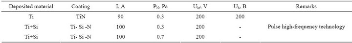
Table 1. Physical and technical parameters of deposition of coatings.
vided on the X-ray diffractometer DRON-3M in Cukα irradiation using graphite monochromator in secondary beam. Diffraction spectrums were obtained in pointwise regime with a scanning step 2θ = 0.05 … 0.10. For stress analysis, we used X-ray tensometry (α-sin2 ψ method) and its modifications, which are valid for coatings with strong axial type texture [12,13].
Elementary composition of the coatings was studied using Rutherford backscattering of 4He+ ions with 1.7 MeV energy, detector resolution E = 13 keV, dispersion angle ≈ 1700. Also we used scanning electron microscopy (SEM) with energy dispersion analysis (Jeol 7000F microscope, Japan) in contrast of electrons and in direct and backscattering electron reflection. For surface morphology investigations, we used atomic-force microscopy AFM Objective to obtain 3D image of surface topography, electron-ion scanning microscope Quanta 200 3D with roentgen-fluorescent microanalyzer EDAX with appropriate software, and automatic contact precision profilometer SURTRONIC 25.
Nanohardness and elastic modulus measurements were done using trihedral Berkovich indentor (Nano Indenter G200, TN, USA, Oak Ridge, Nano Instruments Innovation Center). For analysis of vacancy-type defects in the coating we used slow positron beam (Halle, Germany). We measured S-parameter of the Doppler broadening annihilation peak (DBAP) by changing energy of the fallen positron beam from 1 KeV to 30 KeV, and that allowed us to change the analysis depth [14,15].
The bonding states were determined using photoelectron spectroscopy (XPS, Kratos AXIS Ultra) with a monochromatic AlKα (1486.71 eV, X-ray radiation 15 kV/10 mA).
3. Experimental Results and Discussion
Fragments of diffraction spectrums for Ti-Si-N samples (as deposited and after annealing under the temperature 600˚C for 30 min) are presented on Figure 1. We calculated lattice parameter a0 = 0.42462 A and found strong texture (111) (Ti, Si) N and (222) (Ti, Si) N (see Curves 1 and 2).
In addition, we detected small peaks from TiO2 (JCPDS-19-370). Volume fraction of oxides after thermal annealing in the chamber is low and it is not higher than 5%.
Stresses analysis showed, that there is high compres-
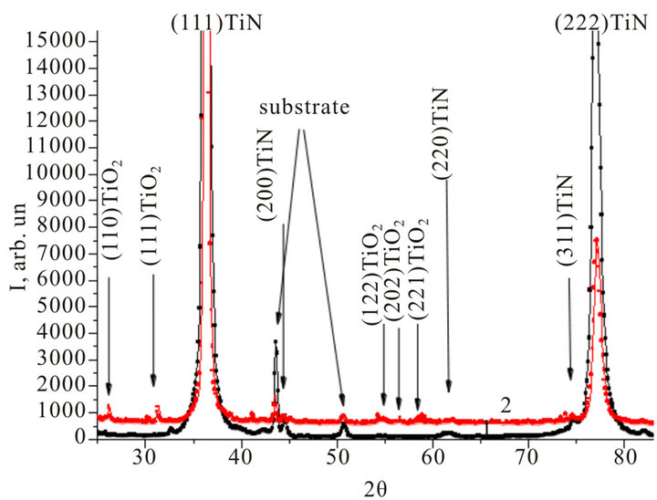
Figure 1. Ti-Si-N coating’s X-ray diffraction patterns: 1) as deposited; 2) after annealing under the temperature 600˚C for 30 min, vacuum P = 50 mbar.
sion deformation in (Ti, Si) N hard solution (equals to −2.6%) and it is reduced to the value of −2.3% after annealing.
Coherent-scattering region evaluation (using Sherrer methodic) showed that size of nanograins increased from 12.5 nm to 13 nm, and when initial size of nanograins is 25 nm, it increased to (28 - 30) nm. In other words, due to annealing under the temperature of 600˚C for 30 minutes, insignificant changing of grain size is observed, and rest part of energy was used on finishing of spinodal segregation process, forming of monolayer α-Si3N4.
We can make an interim conclusion, that when compression deformation and order of structuring are high, annealing under the temperature of 600˚C for 30 minutes do not lead to catastrophic changes both in phase composition, structure and mode of deformation. Layer, made of (Ti, Si)N solid solution, is formed, and silicon-nitrogen phase is also formed around nanograins. In according to it, Si concentration is reduced in solid solution; some amount of Ti atoms creates TiO2 film on the coating’s surface.
Ti-Si-N coatings structure is characterized by high level of microdeformations of lattice (more than 1%) [9]. High value of microdeformations of lattice probably indicates on inhomogeneity of chemical structure in every phase of the coating.
Coatings have strong texture [6]. Condensation compressive stresses leads to (111) texture forming in (TiSi)N solid solution films. Using approximation methods we defined average crystallites sizes of the (Ti, Si)N solid solution, and it varies from 12.5 to 25 nm. The obtained coatings have next hardness: TiN (H = 28 GPa, E = 312 GPa); Ti-Si-N (H = 38 - 39 GPa, E = 356 GPa).
In Table 2, we summarized results of tribological investigations. It is clearly seen from this results, that wear coefficient for TiN coating increases with temperature increasing, but for Ti-Si-N coating wear coefficient decreases to 0.69 (T = 500˚C), which is approximately on 25% less, than under room temperature.
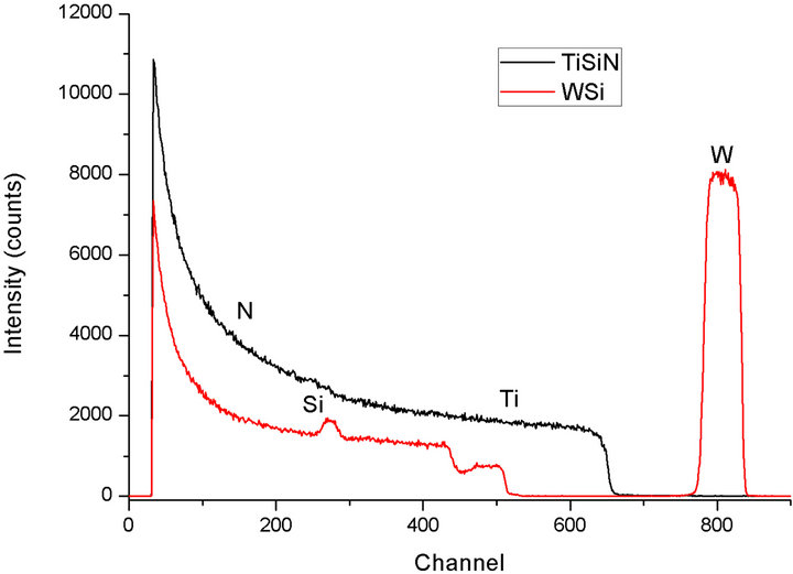
Elementary analysis results are presented on Figure 2, it was obtained using RBS method and EDS (energydispersion spectroscopy). As it is clearly seen from Figure 2(a), Si concentration is less than 5 at.%, N concentration » (35 - 40) at.%, rest one is Ti, and for Figure 2(b) N concentration » 50 at.%, Ti » 44 at.%, Si » 5.5 at.%. Coating’s thickness equals to 2.18 ± 0.01 µm in according to RBS data.
RBS data confirms by EDX results, see Figure 2(c). Concentration of Si in the coating is 2.62 at.%, Ti » 40.69 at.%, N » 55.92 at.%. For another series of samples (with Si concentration ≥ 5.8 at.%) we provided investigations of Si-Nx connection using XPS analysis. It showed high peak on 101.9 eV, and it points directly on forming of Si-Nx connection in this sample. But also we had a small peak, which points on forming of a very few amount of Si-O on 103.9 eV (after annealing in the air under the temperature of 600˚C for 30 min). Additional µ-PIXE investigations showed SiN forming on TiN nanograins borders.
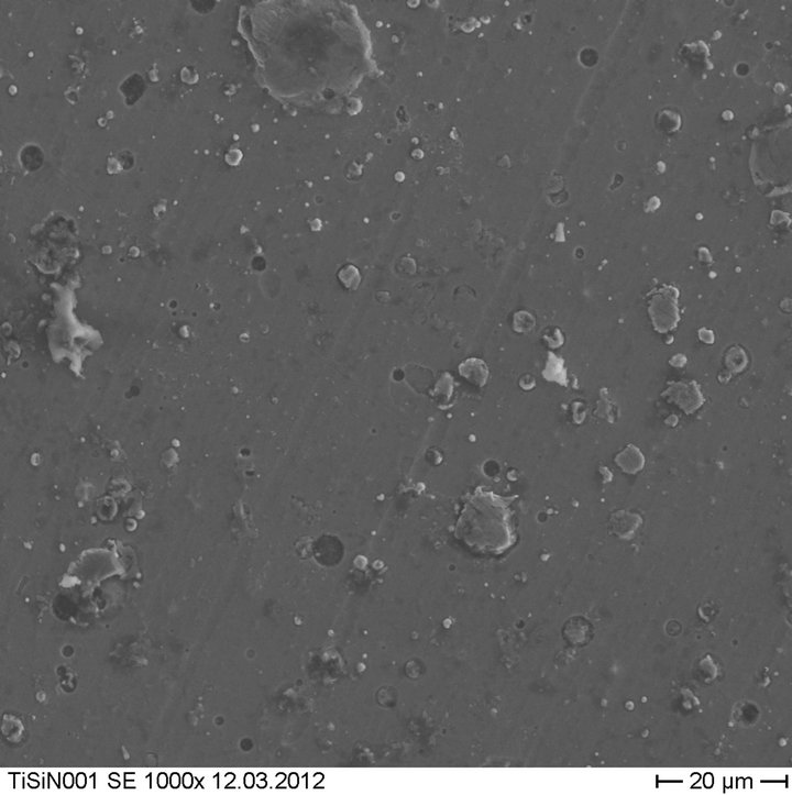
Images of the coating’s surface before and after annealing, under the temperature 600˚C (for 30 minutes) are presented on Figure 3. We can observe flat “drops” of melted phase, no matter of HF stimulation. We should note that part of plasma jet consists of drop fractions, and we did not make analysis of such fractions.
To obtain a real thickness of Ti-Si-N nanostructure coating and to norm the depth of slow positron beam analysis, we cut a circle hole, through the coating thickness. As it is seen from Figure 3(c), coating’s thickness equals to 2.39 - 2.41 µm. Calculation of positrons penetration depth shows that Emax = 20 keV, it corresponds to 2.11 µm of thickness. Even if we will take into account diffusion of thermalized positrons (it length is L » 100 nm), we will see that positron beam cannot reach interface between coating and substrate. That is why profiles of mean positron’s penetration depths give us information about vacancy-type defects on the whole thickness of Ti-Si-N coating, but the interface border is not really achieved by them.
Positron annihilation method is the most effective, responsive and reliable method of analysis of free volumes in nanocrystalline materials (it has possible interval of defect’s analysis in the range 10−6 ± 10−3 defects per atom) [14,15]. Part of positrons can be captured on the interface of two neighboring nanograins or on boundary junction of three neighboring nanocrystals. It gives us good opportunity to solve one of the most complicated and interesting problems of nanomaterials—to understand structure (including electron structure) of the interfaces between nanograins, because length (volume) of such interfaces influences a lot on properties of nanocomposite coatings [1-9].
Figure 4 shows dependence of S-parameter on energy, in other words, we can see profiles of defects in Ti-Si-N coating before (black curve) and after (red curve) thermal annealing under the temperature of 600˚C (30 min).
Significant changes in electron and defect structure of the coating is clearly seen from this figure. We should note, that defects concentration increases on the whole thickness of the coating, all positrons locates and annihilates on defects, which are situated on the boundaries of nanograins. Depth of diffusion of thermolized positrons is » 100 nm, size of nanograins is (12.5 - 13) nm, so we can say that almost all positrons are captured on interface’s defects. As approaching to the interface between coating and substrate, S-parameter significantly increases, i.e. defects also migrate to the interface between coating and substrate due to thermal diffusion. Thickness of this transition layer of defects is no more than 250 nm. Calculation of vacancy defects concentration was done using
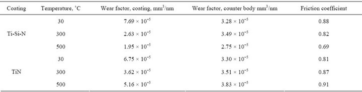
Table 2. Tribological properties of nanocomposite coatings.
 (a)
(a)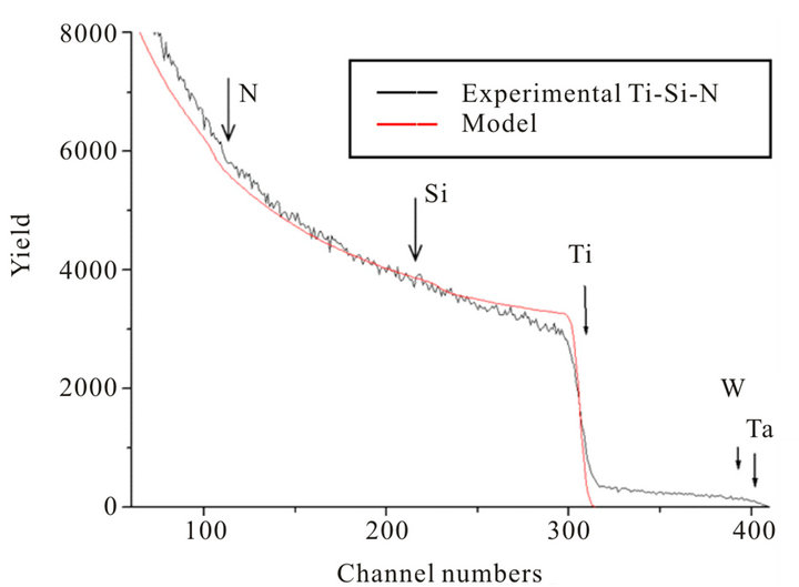 (b)
(b)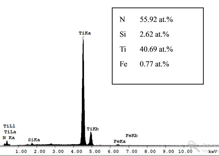 (c)
(c)
Figure 2. Energy spectrums for samples with Ti-Si-N coatings; (a) bias potential −50 V, PN = 0.5 Pa (RBS), second curve corresponds to etalon SiW curve (for comparing); (b) bias potential −100 V, PN = 0.7 Pa (RBS); (c) bias potential −50 V, PN = 0.5 Pa (EDX).
positron capture model with two types of vacancy defects [12], and it showed that defects concentration increases
 (a)
(a)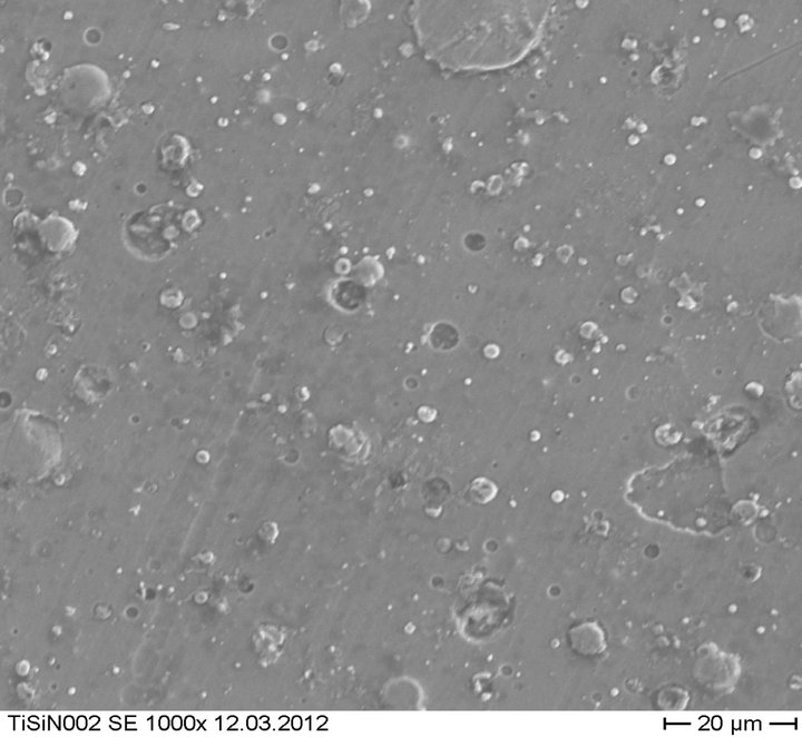 (b)
(b)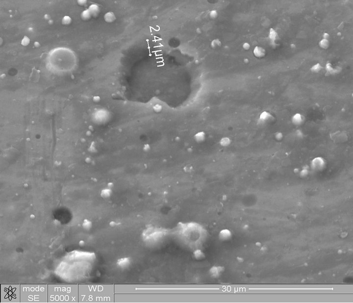 (c)
(c)
Figure 3. Surface topography of the Ti-Si-N coating; (a) as deposited state; (b) after annealing under the temperature of 600˚C; (c) SEM-analysis of circle cross-section, which was obtained using ion beam cutting.
after annealing from 5 × 10¹⁶ to 7.5 × 1017 cm−3, thermally activated vacancies concentration also increases from 1 × 10¹⁶ to 5 × 1018 cm−3 (see red curve).
Loading and unloading curves are presented on Figure 5. Nanoindentor penetrates on the surface layer of the
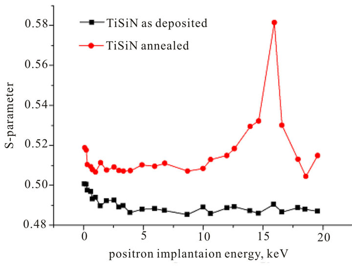
Figure 4. Dependence of S-parameter on energy of positron microbeam (black curve—as deposited coating, red curve—annealed coating).
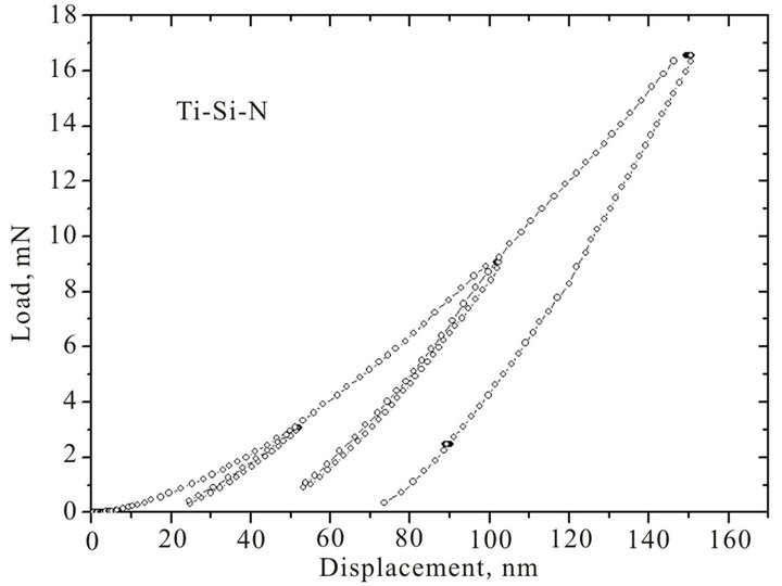
Figure 5. Loading and unloading curves, obtained for Ti-Si-N coating (U = −100 V, Pn = 0.7 Pa), indentation on 50, 100 and 150 nm depth.
Ti-Si-N coating (three different loadings). As it is seen from calculations, based on Oliver-Pharr methodic, an average hardness for such deposition regimes is 38.7 GPa, elasticity modulus is 370 ± 12 GPa. Annealing under the temperature of 600˚C in vacuum leads to increasing of elasticity modulus to values (430 - 448) GPa, it is connected with finishing of process of spinodal segregation on the boundaries of nanograins, i.e. with forming of thin SiN (Si3N4) interlayer (amorphous and quasi amorphous phases).
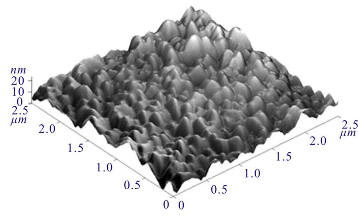
Moreover, thermal annealing under the temperature of 600˚C in vacuum also changes Ti-Si-N coating’s surface morphology (Figure 6).
We observed decreasing of an average roughness size, increasing of amount of defects (it is obvious from Figure 6).
After analysis we can say, that structure of defects
 (a)
(a)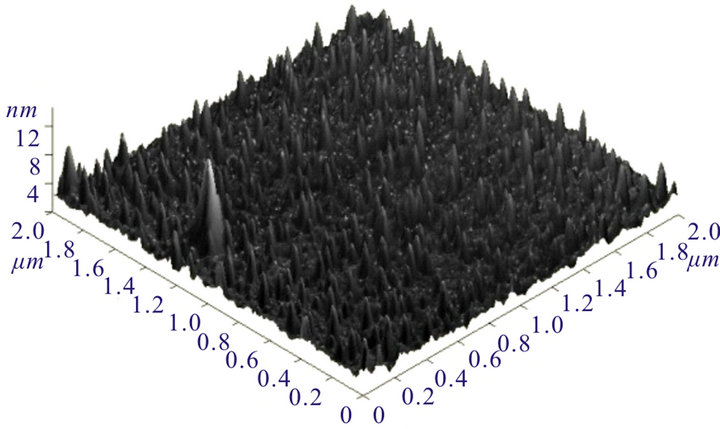 (b)
(b)
Figure 6. Ti-Si-N coating’s surface morphology: (a) 3-d AFM image; (b) after annealing under the temperature of 600˚C.
changes on nanograins interfaces due to annealing, average roughness size decreases, nanohardness increases on 20% (in comparison with as deposited state) and it correlates with our previous works [13,16]. Friction ratio decreases on 25%—it is the main difference as opposed to works [17-19].
4.Acknowledgements
Authors thank M.V. Kaverin (Sumy, Ukraine) for measuring of profiles defects using slow positron beam, G. Abrasonis (Dresden, Germany) for elements’ composition studies using RBS-analysis, V. M. Beresnev (Kharkov, Ukraine), D. A. Kolesnikov (Belgorod, Russia) and R. Krause-Rehberg (Halle, Germany). The work was done under financial support of Ministry of Education and Science of Ukraine (state program, order No. 411), and in collaboration with NIMS (Tsukuba, Japan) and Martin-Luther University (Dresden, Germany). The work was supported by Ministry of Education and Science of Ukraine (project No. 0112U005920) and Ministry of Education and Science of Russia (grant No 12-08-31060). Authors are grateful to the staff of the Joint Research Center “Diagnostics of Structure and Properties of Nanomaterials” (Belgorod State University, Russia) for their assistance with instrumental analysis.
REFERENCES
- Н. Gleiter, “Nanocrystalline Materials,” Progress in Materials Science, Vol. 33, No. 4, 1989, pp. 233-315.
- R. W. Siegel, “Cluster-Assembled Nanophase Materials,” Annual Review of Materials Science, Vol. 21, No. 1, 1991, pp. 559-579.doi:10.1146/annurev.ms.21.080191.003015
- S. Veprek and S. A. Reiprich, “Concept for the Design of Novel Superhard Coatings,” Thin Solid Films, Vol. 268, No. 1-2, 1995, pp. 64-71. doi:10.1016/0040-6090(95)06695-0
- A. D. Pogrebnyak, A. P. Shpak, N. A. Azarenkov and V. M. Beresnev, “Structures and Properties of Hard and Superhard Nanocomposite Coatings,” Physics-Uspekhi, Vol. 52, No. 1, 2009, pp. 29-54. doi:10.3367/UFNe.0179.200901b.0035
- P. H. Mayrhofer, C. Mitterer, L. Hultman and H. Clemens, “Microstructural Design of Hard Coatings,” Progress in Materials Science, Vol. 51, No. 8, 2006, pp. 1032-1114. doi:10.1016/j.pmatsci.2006.02.002
- J. Musil, “Hard and Superhard Nanocomposite Coatings,” Surface and Coatings Technology, Vol. 125, No. 1-3, 2000, pp. 322-330. doi:10.1016/S0257-8972(99)00586-1
- R. A. Andrievski, “Nanomaterials Based on High-Melting Carbides, Nitrides and Borides,” Russian Chemistry Reviews, Vol. 74, No. 12, 2005, pp. 1061-1072. doi:10.1070/RC2005v074n12ABEH001202
- J. Musil, “Hard Nanocomposite Coatings: Thermal Stability, Oxidation Resistance and Toughness,” Surface and Coatings Technology, Vol. 207, 2012, pp. 50-65. doi:10.1016/j.surfcoat.2012.05.073
- A. D. Pogrebnjak, A. G. Ponomarev, A. P. Shpak and Y. A. Kunitskii, “Application of Microand Nanoprobes to the Analysis of Small-Sized 3D Materials, Nanosystems, and Nanoobjects,” Physics-Uspekhi, Vol. 55, No. 3, 2012, pp. 270-300. doi:10.3367/UFNe.0182.201203d.0287
- A. Pogrebnjak, M. Danilionok, V. Uglov, N Erdybaeva, G. Kirik, S. Dub, V. Rusakov, A. Shypylenko, P. Zukovski and Y. Tuleushev, “Nanocomposite Protective Coatings Based on Ti-N-Cr/Ni-Cr-B-Si-Fe, Their Structure and Properties,” Vacuum, Vol. 83, Suppl. 1, 2009, pp. S235-S239. doi:10.1016/j.vacuum.2009.01.071
- A. D. Pogrebnjak, V. V. Uglov, M. V. Il’yashenko, V. M. Beresnev, A. P. Shpak, M. V. Kaverin, N. K. Erdybaeva, Y. A. Kunitskyi, Y. N. Tyurin, O. V. Kolisnichenko, N. A. Makhmudov and A. P. Shypylenko, “Nano-Microcomposite and Combined Coatings on Ti-Si-N/WC-Co-Cr/- Steel and Ti-Si-N/(Cr3C2)75-(NiCr)25 Base: Their Structure and Properties,” Nanostructured Materials and Nanotechnology IV: Ceramic Engineering and Science Proceedings, Vol. 31, 2010, pp. 127-138. doi:10.1002/9780470944042.ch14
- R. Krause-Rehberg and H. S. Leipner, “Positron Annihilation in Semiconductors: Defect Studies”, Springer-Verlag, Berlin Heidelberg, New York, 1999, p. 378.
- A. D. Pogrebnjak, M. V. Il’yashenko, M. V. Kaverin, A. P. Shypylenko, A. V. Pshyk, V. M. Beresnev, G. V. Kirik, N. K. Erdybayeva, N. A. Makhmudov, O. V. Kolisnichenko, Yu. N. Tyurin and A. P. Shpak, “Physical and Mechanical Properties of The Nanocomposite and Combined Ti-N-Si /WC-Co-Cr/ and Ti-N-Si/(Cr3C2)75-(Ni-Cr)25 Coatings,” Journal of Nanoand Electronic Physics, Vol. 1, No. 4, 2009, pp. 66-77.
- A. D. Pogrebnjak, Sh. M. Ruzimov, D. L. Alontseva, P. Zhukowski, C. Karwat, C. Kozak and M. Kolasik, “Structure and Properties of Coating on Ni-base Deposited Using Plasma Jet Before and After Electron Beam Irradiation,” Vacuum, Vol. 81, No. 10, 2007, pp. 1243-1251. doi:10.1016/j.vacuum.2007.01.071
- A. D. Pogrebnjak, “Investigation of Element Profiles, Defects, Phase Composition and Physical and Mechanical Properties of Superhard Coatings Ti-Hf-Si-N,” Materials Science and Applications, 2013, in publishing. doi:10.4236/msa.2013
- A. D. Pogrebnyak, A. M. Mahmud, I. T. Karasha, G. V. Kirik, R. Y. Tkachenko and A. P. Sypylenko, “Structure аnd Physical-Mechanical Properties of Nc-TiN Coatings Obtained by Vacuum-Arc Deposition and Deposition of HF Discharge,” Journal of Nanoand Electronic Physics, Vol. 3, No. 4, 2011, pp. 97-105.
- A. D. Pogrebnjak, V. M. Beresnev, A. A. Demjanenko, V. S. Baidak, F. F. Komarov, M. V. Kaverin, N. A. Makhmudov and D. A. Kolesnikov, “Adhesive Strength, Superhardness and the Phase and Elemental Composition of Nanostructured Coatings Based on Ti-Hf-Si-N,” Physics of the Solid State, Vol. 54, No. 9, 2012, pp. 1882-1890. doi:10.1134/S1063783412090247
- A. D. Pogrebnjak, V. M. Beresnev, A. Sh. Kaverina, A. P. Shypylenko, O. V. Kolisnichenko, K. Oyoshi, Y. Takeda, H. Murakami, D. A. Kolesnikov and M. S. Prozorova, “Formation of Superhard Ti-Hf-Si-N/Nb-N/Al2O3 Multilayer Coatings for Highly Effective Protection of Steel,” Technical Physics Letters, Vol. 39, No. 2, 2013, pp. 189- 192.doi:10.1134/S1063785013020223
- A. D. Pogrebnjak, V. M. Beresnev, D. A. Kolesnikov, M. V. Kaverin, A. P. Shypylenko, K. Oyoshi, Y. Takeda, R. Krause-Rehberg and A. G. Ponomarev, “The Effect of Segregation and Thermodiffusion on the Formation of Interfaces in Nanostructured (Ti-Hf-Zr-V-Nb)N Multie- lement Coatings,” Technical Physics Letters, Vol. 39, No. 3, 2013, pp. 280-283.
NOTES
*Corresponding author.