World Journal of Nano Science and Engineering
Vol.4 No.1(2014), Article ID:43738,9 pages DOI:10.4236/wjnse.2014.41002
Electrical Analysis of Indium Deep Levels Effects on Kink Phenomena of Silicon NMOSFETs
Abdelaali Fargi, Neila Hizem, Adel Kalboussi, Abdelkader Souifi
Department of Physics, Faculty of Sciences of Monastir, Monastir, Tunisia
Email: fargi.abdelaali@gmail.com
Copyright © 2014 by authors and Scientific Research Publishing Inc.
This work is licensed under the Creative Commons Attribution International License (CC BY).
http://creativecommons.org/licenses/by/4.0/


Received 8 June 2013; revised 8 July 2013; accepted 15 July 2013
ABSTRACT
Several methods of characterization of trap levels like I-V, C-V and transient spectroscopy (DLTS) were used to determine the accurate values of the activation energies of traps present in N+P junctions obtained after retrograde profile implantation of indium and boron on silicon. Four main traps located at Ev + 0.15 eV, Ev + 0.21 eV, Ev + 0.28 eV and Ev + 0.46 eV are reported. Shallow levels are also calculated from I-V characteristics. Concurrently, indium channel doped NMOSFETs are investigated showing the kink phenomenon. In order to discuss the relationship between the kink effect and the active indium trap level situated at 0.16 eV, the transient effects are studied by varying the integration time and the temperature. The effects of substrate polarization are also carried out showing the reduction of the kink with the bulk positive polarization.
Keywords:Electrical Characterization; MOSFET; Indium Deep Traps; Kink Effect; Impact Ionization

1. Introduction
Microelectronics’ evolution implies the reduction of the components’ size to improve the density of integration and the rapidity of circuits. The reduction of this size is particularly critical on the channel length under the gate, and leads to several parasitic effects when gate length goes down below 0.1 µm. The control of Short Channel Effects (SCE) becomes more challenging. This often requires a higher substrate doping concentration for effective SCE control. Thus, Retrograded Channel Profile (RCP) formation has been suggested, where a high substrate doping concentration is buried underneath the surface, leaving a lightly doped region at the surface [1] . The lightly doped Si surface results in less ionized impurity scattered in the channel, and this improves the electron mobility that is dominated by surface scattering. The highly doped region buried underneath the surface limits the gate depletion width, and therefore reduces the amount of SCE [2] . In order to build a NMOS Transistors with retrograde channel, indium seems to give the best profiles that are sufficiently fine and not very sensitive to annealing. It seems obvious that its heavy ion is less diffused allowing indium to give narrow profiles [3] . However, indium’s mass, which is a quality for reaching retrograde profiles, will be a defect when indium becomes electronically active. Another problem arises: indium precipitates as soon as the concentrations exceed 1017 cm−3 [9] . Even with the advantages of indium doped silicon, when scaling down dimensions of MOSFETs, many parasitic effects appear such as the kink effect. This parasitic effect, which is characterized by a sharp increase in the drain-source current at a certain drain-to-source voltage (Vds = Vkink), yields a high drain conductance. Many studies of the kink effect in field effect transistors such as MOSFETs (bulk and SOI) and HEMTs have been reported. However, due to its complex behavior, the origin of this effect is still a subject of interest. Some studies have established a link between the kink effect and the impact ionization phenomenon occurring in the channel [4] , while other studies have correlated this effect with the presence of traps in the structure [5] . Other studies such as [6] have reported that the impact ionization depends on a hole trapping and detrapping phenomenon in HEMTs. The surface states can also affect the kink phenomenon as shown in GaAs MESFETS [7] . However, few works have been reported on how the deep trap affects the kink in Si MOSFETs. The aim of this work is to discuss the relative influence of the kink effect compared to the ionization of indium levels in silicon. A detailed study of the electrical properties of deep levels was performed in N+P junctions using I-V-T, C-V-Tandtransient spectroscopy (DLTS) techniques. In order to study the impact of deep trap levels on the kink effect, drain current measurements were carried out in the 100 - 350 K temperature ranges. The substrate-related kink dynamics are also analyzed.
2. Experimental Details
N+P well diodes and NMOSFET transistors were fabricated to study the effect of dopant redistribution. These devices were investigated in each case using a retrograde well indium and boron implantation as shown in Figure 1 which was deduced from capacitance-voltage profiling. A P well of about 5 × 1017 cm−3 indium implanted, was formed in a P substrate at 100 nm under the interface. Boron implantation was performed to adjust the substrate doping to about 1017 cm−3. The NMOSFET device had a gate oxide thickness of 3.2 nm. The surface of the active zone of the poly gate NMOSFETs was 100 × 100 µm2 (L × W). N+P well diodes fabricated with 5 × 1016 cm−3 for both In and B dopants were used for testing the MOS devices. A variety of methods, DLTS and I-V-T, have been used to characterize the acceptor levels related to the presence of Indium in N+P well diodes and MOS transistors.
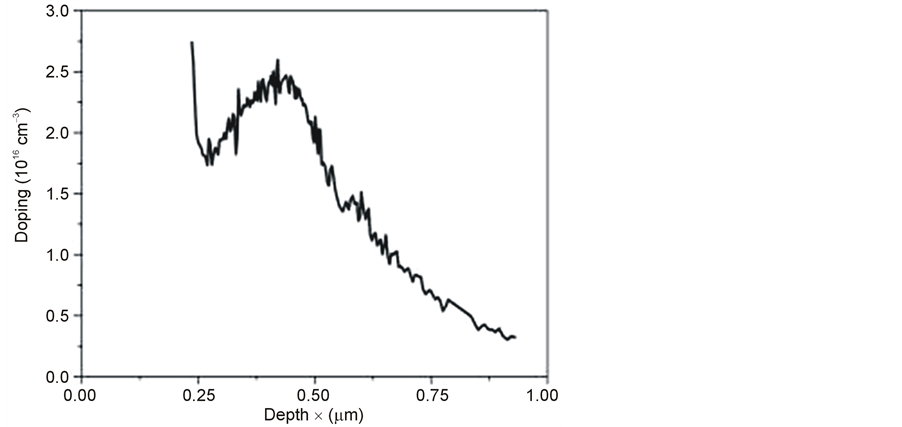
Figure 1. Retrograded doping profile showing indium and boron concentration deduced from Capacitance-Voltage profiling.
3. Diode Results
3.1. I-V-T Measurements
The current-voltage I-V characteristics of N+P well diodes have been measured over a wide range of temperature (80 - 300 K). Some intrinsic and contact properties such as barrier height Vd = 0.7 V, ideality factor n = 1.7, and series resistance Rs = 14 Ω were calculated from the forward current-voltage characteristics at room temperature. Figure 2, shows reverse current-voltage characteristic of a diode as a function of temperature. If the reverse current is related to traps generation from a deep level in the space charge region, the activation energy could be determined from ln(I/T5/2) versus 1000/T plot [8] .
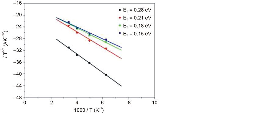
The analysis of the Arrhenius plots at different reverse polarizations reported in Figure 3, shows two straight lines; one for temperature higher than 170 K that gives activation energies between 0.15 - 0.28 eV (Figure 3(a)) and the second one gives activation energies between 66 - 23 meV for temperature lower than 170 K (Figure 3(b)). The activation energy values are reported in Table 1.
3.2. C-V-T Measurements
In order to investigate the freeze-out of carriers and the presence of the hole traps, Figure 4, shows the capacitance voltage as a function of temperature varying between 80 and 300 K at frequency 100 KHz. The dispersion of curves with temperature at zero bias is due to deep defect levels the density of which decreases when the depth increases.
Finally, we don’t observe any anomaly in C-V curves even at a low temperature. In fact, all indium atoms are electrically active. Since Cerofolini et al. [9] observed that with an In concentration below 1017 cm−3 the junction is electrically active while with a concentration > 1017 cm−3 evidence for precipitation as the mechanism responsible for inactivation was given.
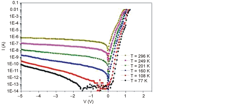
Figure 2. The reverse current-voltage characteristics at different temperature of N+P diode.

Table 1. Thermal activation energies of shallow and deep traps extracted from I-V-T measurements.
 (a)
(a)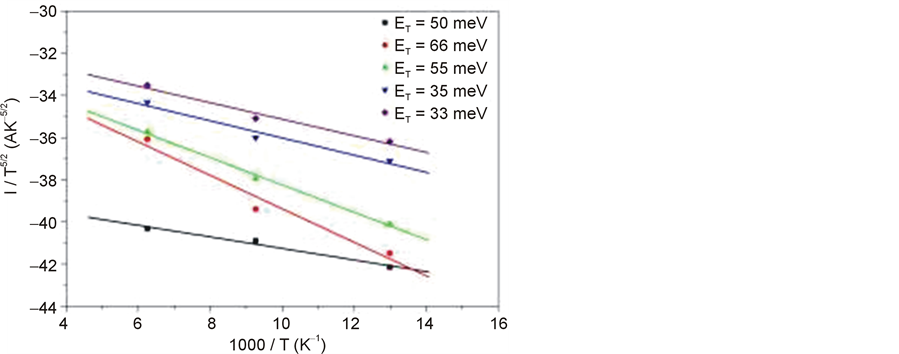 (b)
(b)
Figure 3. The analysis of the Arrhenius plots at different polarization: (a) For temperature upper than 170 K, (b) For temperature less than 170 K.
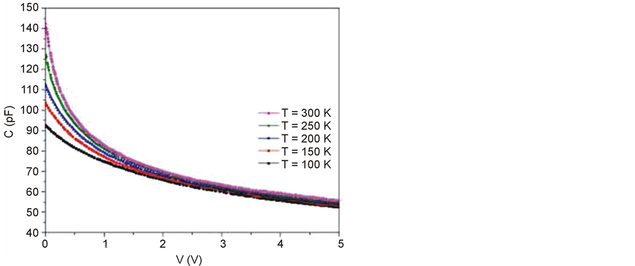
Figure 4. Capacitance-Voltage versus temperature of N+P junction at frequency f = 100 KHz.
3.3. DLTS Measurements
DLTS measurements, as shown in Figure 5, were performed in 40 - 300 K temperature range and made by lock-in amplifier technique (A-B) for different emission rates. Two main activation energy values 0.18 eV and 0.45 eV are extracted from the Arrhenius plot. A comparative study for the same temperature range of DLTS results with I-V measurements and later works revealed that the trap level located at 0.18 eV seems to be in good agreement with the 0.15 - 0.2 eV observed by I–V measurements and the 0.16 eV indium level measured by different characterization techniques: DLTS [10] , Hall Effect [9] , and Infrared Absorption [11] . The variety of values of in deep trap detected by different techniques is explained by the electric field effects due to coulomb traps [10] .
4. MOSFET Results
4.1. Ids-Vds Characteristics
The Figure 6 shows the static output characteristics (Id-Vd) of the transistor at different gate voltages. We notice that the drain current continues to increase even in the saturation region. This unusual variation of the drain current is well known as the kink effect [12] . It consists of a sharp increase in the drain/source current at a certain drain-to-source voltage (Vd = Vkink). This variation of the drain current induces an increase of the drain/source output conductance (gds) and a decrease of the amplification factor. We observe that when the gate voltage increases, the amount of drain current and kink voltage (Vkink) increases too. The kink voltage seems to begate voltage dependent.
4.2. Kink Analysis
As seen in Figure 7, the pre-kink zone is highly temperature dependant. When the temperature decreases from 300 K the kink phenomena is more pronounced with a clear increase of the amount of drain current especially around 100 K where the In trap appears.
The trans conductance is maximal at the temperature range of indium deep trap appearance as shown in Figure 8. After the Vkink voltage the curves are identical. Therefore one concludes that the kink effect is related to the trapping and detrapping of the deep traps in the pre-kink region.
In order to get a better understanding of the influence of the deep traps were port in Figure 9, the changes of the Id-Vd characteristics when the drain voltage is swept by long, medium and short speeds. When the integration time is short the kink tends to disappear and the drain current is higher than that of longer integration time.
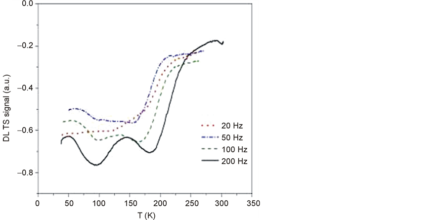
Figure 5. DLTS signal of N+P junction for reverse bias Vr = −4 V and pulse bias Vp = 0 V, with different emission rates.
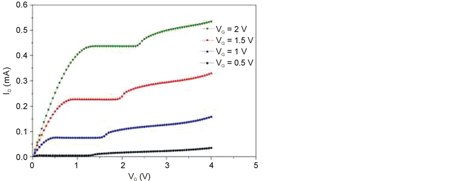
Figure 6. The output Id-Vd characteristics at room temperature of NMOSFET transistor.
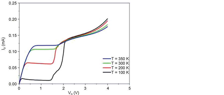
Figure 7. The output Id-Vd characteristics in the temperature range between 100 and 350 K.
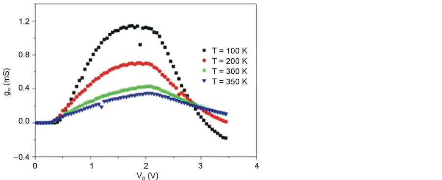
Figure 8. The temperature dependence of the transconductance-drain voltage characteristics.
This is because of the presence of hole traps that find enough time to capture injected electrons in thechannel when the integration time is longer resulting in are duced drain current. No changes in the characteristics for Vd > Vkink.
Next, we describe changes of the Id-Vd characteristics when bulk polarization varies from −1 V to +2 V, at room temperature. Figure 10, shows the reduction of the kink with positive polarization of the bulk. If we compare the curves before and after the Vkink tension we will find that for Vd < Vkink the drain current increases with the increasing of Vsub, but for Vd > Vkink the drain current curves are confound with different bulk polarizations.
The inside shows that the pre-kink zone is sensitive to substrate polarization. The drain current rises and gets saturated at bulk positive polarization (Vsub > +0.5 V) for Vd = 1.28 V < Vkink, and Vg = 1.5 V. The drain current increase and the Kink effect reduction are related to the activation process of the indium deep level in the space charge region. We believe that at Vg = 1.5 V, for negative bulk polarization the space charge region be-comes larger and the capture process increases, a low drain current and a strong kink effect occur. For positive bulk polarization the space charge zone is reduced, the trapping phenomenon decreases and the kink is also reduced. This confirms the relation between the trap level and the kink effect.
The kink has also been reported in other devices such as SOI MOSFETs [13] [14] , GaAs-based and InP-based HEMTs [15] -[17] , etc. In the SOI MOSFETs, the kink is considered to occur due to the floating body effects and the parasitic bipolar effects originated from impact ionization of holes. In the HEMTs, impact ionization is
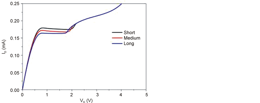
Figure 9. The changes of the transient effect with short long and medium integration time during data acquisitions.
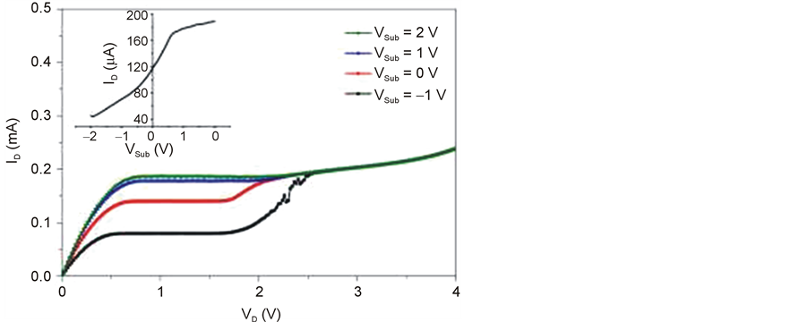
Figure 10. The effects of substrate polarization at 300 K. The inset shows the drain current-substrate voltage in the pre-kink zone (Vd = 1.28 V, Vg = 1.5 V).
believed to be a necessity for the kink, and some traps should be correlated to it. Some other works conclude that both impact ionization and trapping and detrapping by a deep level centre are responsible for kink effect [18] [19] .
In this work, the analysis of the kink effect from the Id-Vd characteristics leads to think that two different phenomena arise before and after Vkink voltage. Before Vkink we expect that the drain current behavior according to the temperature, the bulk polarization and integration time dependence is correlated to the incomplete ionization of the indium trap level. This trap can capture the electrons injected in the channel causing a reduction of the drain current. In contrast the drain current increase after the Vkink when Vd increases doesn’t present any dependence on temperature or substrate polarization nor on integration time. This is probably correlated to the impact ionization effect. Indeed by increasing the voltage Vds beyond the pinch-off voltage, the drain field becomes strong enough to ionize atoms in the space charge area channel at the drain side. These highly energetic electrons are able to extract other electron-hole pairs even at low temperature. The created electrons contribute strongly to the conduction channel. The holes are attracted towards the gate, but others are attracted to the substrate thus causing a gate-substrate current resulting in an increase of the drain current too [20] -[22] .
5. Conclusion
Indium deep traps have been performed by I-V-T and DLTS measurements. It has been shown that indium induces two distinct levels: a shallow level at 20 meV and a deep one at 0.18 eV with electric field dependence. Electrical properties of NMOSFET transistors were characterized. The kink effect in MOSFET devices has been examined using temperature, bulk polarization and integration time. The incomplete ionization of indium could be the main origin of the kink effect. Depending on the temperature and the substrate polarization, the pre-kink region is changed, resulting in the change of the amount of the drain current. This behavior is mainly related to the presence of deep electron traps. Therefore, the non saturation of the drain current after the kink zone could be related to the impact ionization. This leads to concluding that both the impact ionization effect and trapping/ detrapping by a deep level center are responsible for the increase of drain current. Transient and dynamic simulations have indicated that the kink phenomena originated from interaction between generated electrons and deep levels should be rather slow processes with long response times.
References
- De, I. and Osburn, C.M. (1999) Impact of Super-Steep-Retrograde Channel Doping Profiles on the Performance of Scaled Devices. IEEE Transactions on Electronic Devices, 46, 1711-1717. http://dx.doi.org/10.1109/16.77716
- Skotnicki, T., Guérin, L., Mathiot, D., Gauneau, M., Grouillet, A., D’Anterroches, C., André, E., Bouillon, P. and Haond, M. (1994) Channel Engineering by Heavy Ion Implants. 24th ESSDRC, 94, 671-674.
- Ong, S.Y., Chor, E.F., Leung, Y.K., Lee, J., Li, W.S., See, A. and Chan, L. (2002) Steep Retrograde Indium Channel Profiling for High Performance nMOSFETs Device Fabrication. Microelectronics Journal, 33, 55-60. http://dx.doi.org/10.1016/S0026-2692(01)00104-5
- Martinot, H. and Rossel, P. (1971) Carrier Multiplication in the Pinchoff Region of m.o.s. Transistors. Electronics Letters, 7, 118-120. http://dx.doi.org/10.1049/el:19710078
- Ben Salem, M., Bouzgarrou, S., Sghaier, N., Kalboussi, A. and Souifi, A. (2006) Correlation between Static Characteristics and Deep Levels in InAlAs/InGaAs/InP HEMT’S. Materials Science and Engeineering B, 127, 34-40. http://dx.doi.org/10.1016/j.mseb.2005.09.047
- Zaman, S. and Parker, A. (2007) Impact Ionization Dependence of Hole Trapping Phenomena in Hemts. Journal of Science and Technology, 2, 8-12. http://dspace.daffodilvarsity.edu.bd:8080/bitstream/handle/123456789/460/Impact%20ionization.pdf?sequence=1
- Horio, K., Wakabayashi, A. and Yamada, T. (2000) Two-Dimensional Analysis of Substrate-Trap Effects on Turn-On Characteristics in GaAs MESFETs. IEEE Transactions on Electronic Devices, 47, 2270-2276. http://dx.doi.org/10.1109/16.824738
- Lançon, R. and Marfaing, Y. (1969) Mécanisme de génération-recombinaison dans les jonctions p-n de tellurure de cadmium. Le Journal de Physique, 30, 97-102. http://dx.doi.org/10.1051/jphys:0196900300109700
- Cerofolini, G.F., Pignatel, G.U., Mazzega, E. and Ottaviani, G. (1985) Supershallow Levels in Indium-Doped Silicon. Journal of Applied Physics, 58, 2204-2207. http://dx.doi.org/10.1063/1.335988
- Jones, C.E. and Johnson, G.E. (1981) Deep Level Transient Spectroscopy Studies of Trapping Parameters Forcenters in Indium-Doped Silicon. Journal of Applied Physics, 52 5159-5163. http://dx.doi.org/10.1063/1.329416
- Parker, G.J., Brotherton, S.D., Gale, I. and Gill, A. (1983) Measurement of Concentration and Photoionization Cross Section of Indium in Silicon. Journal of Applied Physics, 54, 3926-3929. http://dx.doi.org/10.1063/1.332566
- Nakahara, M., Iwasawa, H. and Yasutake, K. (1968) Anomalous Enhancement of Substrate Terminal Current beyond Pinch-Off in Silicon N-Channel MOS Transistors and Its Related Phenomena. Proceedings of IEEE, 56, 2088-2090. http://dx.doi.org/10.1109/PROC.1968.6810
- Choi, J.Y. and Fossum, J.G. (1991) Analysis and Control of Floating-Body Bipolar Effects in Fully Depleted Submicrometer SOI MOSFET’s. IEEE Transactions on Electronic Devices, 38, 1384-1391. http://dx.doi.org/10.1109/16.81630
- Valdinoci, M., Colalongo, L., Baccarani, G., Fortunato, G., Pecora, A. and Policicchio, I. (1997) Floating Body Effects in Polysilicon Thin-Film Transistors. IEEE Transactions on Electronic Devices, 44, 2234-2241. http://dx.doi.org/10.1109/16.644643
- Canali, C., Paccagnella, A., Pisoni, P., Tedesco, C., Telaroli, P. and Zanoni, E. (1991) Impact Ionization Phenomena in AlGaAs/GaAs HEMTs. IEEE Transactions on Electronic Devices, 38, 2571-2573. http://dx.doi.org/10.1109/16.97428
- Hori, Y. and Kuzuhara, M. (1994) Improved Model for Kink Effect in AlGaAs/InGaAs Heterojunction FET’s. IEEE Transactions on Electronic Devices, 41, 2262-2267. http://dx.doi.org/10.1109/16.337437
- Suemitsu, T., Enoki, T., Sano, N., Tomizawa, M. and Ishii, Y. (1998) An Analysis of the Kink Phenomena in InAlAs/InGaAs HEMT’s Using Two-Dimensional Device Simulation. IEEE Transactions on Electronic Devices, 45, 2390-2399. http://dx.doi.org/10.1109/16.735714
- Bouzgarrou, S., Sghaier, Na., Ben Salem, M., Souifi, A. and Kalboussi, A. (2008) Influence of Interface States and Deep Levels on Output Characteristics of InAlAs/InGaAs/InP HEMTs. Materials Science and Engineering C, 28, 676- 679. http://dx.doi.org/10.1016/j.msec.2007.10.075
- Sornerville, M.H., Del Alamom J,A. and Hoke, W. (1996) Direct Correlation between Impact Ionization and the Kink Effect in InAlAs/InGaAs HEMTs. IEEE Electron Device Letters, 17, 473-475. http://dx.doi.org/10.1109/55.537079
- Hafez, I.M., Ghibaudo, G. and Balestra, F. (1990) Reduction of Kink Effect in Short-Channel MOS Transistors. IEEE Electron Device Letters, 11, 818-821. http://dx.doi.org/10.1109/55.46953
- Chen, S.S., Lin, S.C. and Kuo, J.B. (1996) Kink Effect on Subthreshold Current Conduction Mechanism for N-Channel Metal-Oxide-Silicon Devices. Journal of Applied Physics, 80, 5821-5827. http://dx.doi.org/10.1063/1.363729
- Huang, C. and Gildenblat, S. (1990) Measurements and Modeling of the N-Channel MOSFET Inversion Layer Mobility and Device Characteristics in the Temperature Range 60 - 300 K. IEEE Transactions on Electronic Devices, 37, 1289-1300. http://dx.doi.org/10.1109/16.108191