Journal of Sensor Technology
Vol.1 No.4(2011), Article ID:8943,9 pages DOI:10.4236/jst.2011.14014
Improvement of High Dynamic Range Capacitive Displacement Sensor by a Global Planarization
Department of Mechanical Engineering, Postech, Korea (South)
E-mail: wkmoon@postech.ac.kr
Received August 1, 2011; revised September 21, 2011; accepted October 10, 2011
Keywords: High Dynamic Range, Capacitive Displacement Sensor, Planarization, Contact Method
Abstract
This study presents an improvement of high dynamic range contact-type capacitive displacement sensor by applying planarization. The sensor is called the contact-type linear encoder-like capacitive displacement sensor (CLECDiS), is a nano-meter-resolution sensor with a wide dynamic range. However, height differences due to patterned electrodes may cause a variety of problems or performance degradation. In devices of two glass wafer surfaces with patterned structures assembled face-to-face and in sliding contact, the heights of the patterns crucially affect their performance and practicality, so it should be planarized for reducing the problem. A number of techniques for planarizing glass wafer surfaces with patterned chrome electrodes were evaluated and the following three were selected as adequate: lift-off, etch-back, and chemical mechanical polishing (CMP). The fabricated samples showed that CMP provided the best planarization. CMP was successfully employed to produce CLECDiS with improved signal reliability due to reduced collisions between electrodes.
1. Introduction
Capacitive sensors are simple, cost-effective, and highly sensitive. They have been widely used for various types of measurements, including position, vibration, surface profile, force, acceleration, pressure, and liquid level measurements [1,2]. However, their measurable range is not sufficiently large for several applications. Some research groups have proposed and studied an encoder-type areavarying capacitive sensor called a “comb-type” sensor [3-8] in order to expand the measurable range. However, although the comb-type sensor has the advantage of providing a high dynamic range, its sensitivity is lower than most conventional gap-varying capacitive sensors. It is difficult to maintain a small constant gap in the combtype sensor, and the resulting non-linear effect (called the “fringe effect”) cannot be ignored. In order to improve the sensor’s resolution, a new comb-type displacement sensor called the contact-type linear encoder-like capacitive displacement sensor (CLECDiS) was proposed by Kim et al. [9,10]. By employing a contact method, the CLECDiS significantly increases the comb-type sensor’s sensitivity to a level comparable to that of high-resolution gap-varying sensors.
However, the device has a short life span, possibly because of the abrasion that occurs during contact-sliding motion due to the height difference between the surfaces of the wafer and electrode [11]. Therefore, if the reason is correct, in order to circumvent this short life span, the sensor should be planarized to reduce the height difference. To the best of our knowledge, this kind of planarization never has been tried for the contact device. In this study, therefore, performance of CLECDiS is improved through applying a planarization method to the sensor. In here, techniques for the planarization were evaluated as the following: lift-off, etch-back, and chemical mechanical polishing (CMP), because they are most widely used methods for a global planarization.
2. Definition of Planarization
The CLECDiS is a capacitive sensor with a large measurement range and high resolution. It is an area-variation type sensor with periodic electrodes for use in an encoder, and uses a contact mechanism to maintain a small gap [9]. This concept is shown in Figure 1. The CLECDiS, which uses counting the period of the signal of an encoder and measuring its analog level together, has very
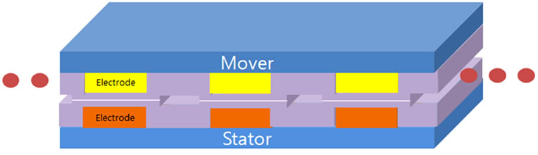
Figure 1. Conceptual diagram of CLECDiS.
small gap; hence its dynamic range is large. However, the sensor has short life span. We believe that the reason of this is due to a contact problem. The contact method of CLECDiS may create problems such as collisions between electrodes in operation. This problem would not occur if the surface of a CLECDiS device were perfectly flat. However, this is not the case for a real CLECDiS device, as shown in Figure 1. In this section, the problem with the contact method is described in detail.
2.1. Description of the Problem
The contact problem studied in this paper may be a problem that occurs not only in a CLECDiS device but also in other contact devices. A contact device has a surface that contacts another surface of another part of the device, and these surfaces involve relative motion. Generally, contact devices have wear problems due to friction.
If the contact device has finite-height patterns that are formed perpendicularly to the moving direction, the problems due to friction will generally be larger. Moreover, the patterns do not merely affect the surface roughness; they may form geometric steps (an example is the CLECDiS shown in Figure 1). In such cases, the problem may not be limited to wear by friction as collisions may occur between the patterns on the contact surface because of the steps. From the perspective of the device, this increases friction dramatically. Collisions always occur in contact sliding devices if the devices form steps with finite height. Some potential causes are shown in Figure 2.
First, Figure 2(a) shows a case in which the patterns have different heights. This may occur after deposition and etching processes because these processes are not perfectly uniform over the entire wafer surface. However, the height differences range from the sub-nanometer scale to about several nanometers, where the steps are hundreds of nanometers in height. These differences are usually smaller than surface roughness, which is usually about (or below) 10 nanometers in size. Hence, they may have smaller effects on the sensor than the roughness. Therefore it is not considered important here.
A second reason for collisions is that the device substrate is not perfectly planar. All wafers have a finite value of total thickness variation (ttv)/bow/warp, making the substrate a non-flat plate. Furthermore, the substrate
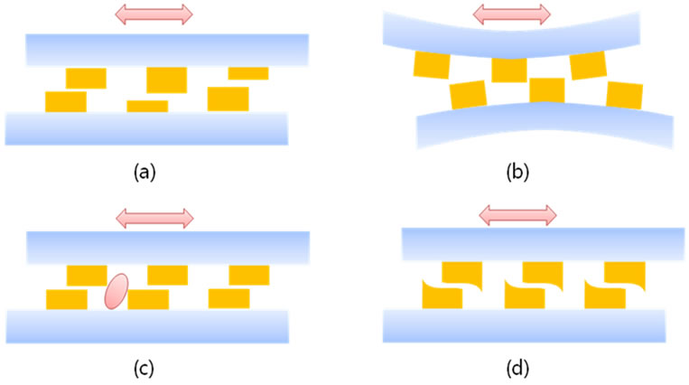
Figure 2. Four cases of pattern collision in contact devices. Possible reasons for collision include the following: (a) thickness differences due to deposition error, (b) substrate nonplanarity caused by bending in some fabrication steps and total thickness variation (ttv)/bow/warp of a wafer, (c) particles attached to the substrate or the electrode, and (d) electrode edge deformation that occurred during fabrication.
is bent by residual stress in some fabrication steps. Figure 2(b) illustrates this collision concept. The effect of the geometrical non-planarity of the substrate can be reduced when the device is small, because the effect is dependent on the size. If the ttv of a 1.524-mm (0.06 in.)-thick wafer is 2 μm, then the ttv of a 1.524 mm device is expected to be approximately 20 nm. If the device is sufficiently small, the effect may be ignored. However, a sensor with a size exceeding several millimeters, such as a CLECDiS, cannot ignore the geometrical non-planarity of the substrate if the sensor is of the contact type. In practice, the effect may not occur in concave areas, although it occurs in convex areas. Therefore, the effect of the steps should be smaller than that of the roughness in convex areas. As this can be achieved by reducing the heights of the steps, the problem may be solved by planarization.
A third consideration is the effect of particles that can cause collisions (Figure 2(c)) or worsen the roughness. Moreover, the electrical characteristics of a device may change if the device is contaminated by charged particles. There are two different types of particle pollution: pollution after fabrication and pollution during fabrication. The effect of the latter can be reduced by cleaning processes before the final coating process. Clearly, the cleaning processes should not harm the device’s metal pattern; hence, processes such as ultrasonic and acetone cleaning treatments are used. However, it is difficult to reduce the effects of particle pollution after fabrication, because the attachment of particles to the sensor surface during its use is unavoidable. Therefore, to reduce the effect of particles, the steps of the pattern should be reduced. If the step heights are reduced, the particles may cause fewer collisions. If the steps are removed, the particles simply scratch the sensor surface. However, this effect can be reduced by using a surface material with high hardness and a low friction coefficient. That is, the effect of particles can be reduced by planarization.
Figure 2(d) shows a fourth case—an electrode with deformed geometry, which in this case is a protruded deformation. It is rare to deform the edge of an electrode in the patterning process. However, residual stress after each fabrication step or collisions can cause this to occur, and small deformations are then made larger through continuing collisions.
These problems are all connected to the problem that the sliding contact surface has steps whose height is larger than the surface roughness, such that the part can be separated clearly from its substrate. The most effective method to solve the problem is to planarize the surface. Naturally, this must be done so as to maintain the electrical characteristics of the electrode pattern while removing its steps. Thus, this study confirmed the effects of applicable planarization methods.
2.2. Definition of Planarization
Planarization may refer to a process or procedure by which a device is fabricated to satisfy a required degree of flatness as well as its outcome. Therefore, it may have various and relative meanings according to the need. Flatness is a geometrical condition that is distinct from roughness. Roughness is quantified by the vertical deviations of the real form of a surface from its ideal form [12]; in contrast, flatness is quantified by the vertical deviations of the real form of a surface from a perfectly flat surface. If the ideal form we wish to obtain is a perfectly flat surface, roughness and flatness are hardly distinguishable. In this study, planarization refers to the result that the level of the flatness is controlled to the level of the roughness. Therefore, the patterned part of the electrode is hardly distinguishable from its substrate by measuring only surface roughness. For example, if a device has a roughness of 10 nm, the planarized device will have a flatness of approximately 10 nm.
Planarization has to be applied to the entire surface of a device; otherwise, the remaining electrode heights of the device might cause collisions. Generally, a wafer has many devices all around its surface. Thus the application of planarization to the entire wafer is simpler than applying planarization to each device. Planarization of the entire wafer, or global planarization, was performed in this study.
3. Planarization Methods
There are numerous studies on planarization. However, most global methods planarize a single material layer. Four methods are usually used for planarization. These are the spinning, lift-off, etch-back, and Chemical Mechanical Polishing (CMP) methods. The spinning method (such as that using Spin-On-Glass) is used for a single material layer and accomplished by depositing liquid on the material and spinning it. Therefore, only the lift-off, etch-back, and CMP methods are used to planarize a patterned surface. This study applies these methods to the planarization of CLECDiS. This section introduces the three methods.
3.1. Lift-Off
Lift-off is a well-known micromachining technique used for patterning [13]. A normal lift-off process is shown in Figure 3(a). A planarization method using lift-off differs in only one way (etching a substrate before depositing a metal) from the normal lift-off method. A lift-off planarization process is shown in Figure 3(b). The first step involves preparing the substrate. The next involves depositing a photoresist (PR) for the sacrificial layer onto the wafer and patterning the PR to create the desired inverse pattern. Subsequently, an etching process creates the desired pattern on the wafer, and metal is filled into the electrode grooves (the etched area on the wafer) down to their full depths. In the present study, the metal used was chrome. The third step is to remove the sacrificial layer. Following this step, only the desired pattern is filled with the remaining metal. The surface of the pattern is also planarized if the thickness of the metal and the depth of the etched part of the wafer are the same.
There are two rules for fabrication. First, the metal should not be deposited on the wall in steps involving metal deposition. It should only be deposited on top of the surface using a method such as an e-beam; otherwise, sharp protrusions may form on both sides of the top. The second rule is that the deposition thickness of the metal must be identical to the patterned depth of the glass. If these are unequal, the patterned surface will not be flat.
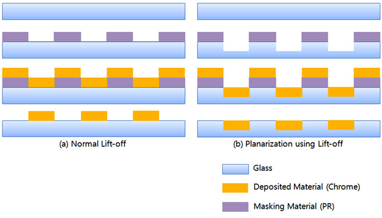
Figure 3. Lift-off method. (a) is a normal lift-off process, and (b) is a planarization process using lift-off.
As a test sample, we used a quartz glass wafer (6 in. in diameter and 0.7 mm thick) as our substrate. The depth of the grooves in the wafer was 120 nm, and the thickness of the deposited metal layer was 120 nm. A glass etcher was used for glass etching and an e-beam evaporator was used to deposit the metal.
3.2. Etch-Back
Etch-back is a widely used planarization method [14-16]. Although the method can be applied in a variety of ways, the basic concept involves etching some (or all) of the extruded areas to make a flat surface using an etchant. The etch-back process used in this study is shown in Figure 4.
The first step involves preparing a wafer and patterning it to create grooves. The next step requires filling the grooves with metal. The deposition thickness of the metal and the depth of the groove should be identical, just as in the lift-off method. Third, a material is deposited onto the metal layer to create a passivation layer. After deposition, the passivation layer is etched into a pattern. This pattern must have the same geometry as the grooves in the wafer because the pattern of the passivation layer can cover all areas in the lower part of the metal layer. This step helps ensure that the protruded part of the metal layer is selectively etched. The next step is to etch the metal layer until the surface height of the protruded metal layer becomes identical to the vertical position of the surface of the lower part. The final step involves removing the PR.
There are three precautions to consider when implementing this method. The first involves taking care that the deposition thickness of the metal is the same as the depth of the etched grooves in the wafer. If these are not identical, the patterned surface will not be flat. The second concerns the need to ensure that the passivation layer
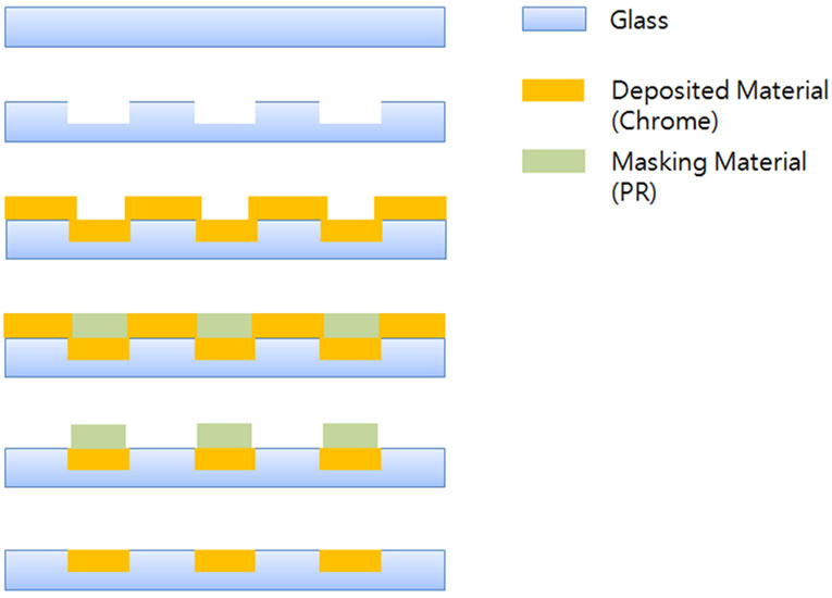
Figure 4. Etch back process.
covers all parts of the wafer to be protected from etching, especially those which are lower than the metal layer. If the coverage is insufficient, some parts of the desired pattern will be removed. The final precaution is to ensure that the metal layer is properly etched, just until the top surface of the wafer appears.
As a test sample, we used a quartz glass wafer (6 in. in diameter and 0.7 mm thick) substrate. The depth of the grooves in the wafer was 120 nm, and the thickness of the deposited metal layer was 120 nm. A glass etcher was used for glass etching and an e-beam evaporator was used to deposit the metal.
3.3. Chemical Mechanical Polishing (CMP)
Chemical Mechanical Polishing (CMP) was originally a surface polishing method for glass wafers [17]. Recently, the method has been used to planarize various fabrications, especially with copper patterning [18-23]. CMP is basically an etching method that uses a mechanical polishing process and a chemical reaction with slurries. The method has low material selectivity, although the chemical slurry and geometry of the polishing pad affects the precision of etching. This means that the target is etched almost uniformly throughout the entire surface. The method is good for global planarization but poor for local planarization or etching.
The traditional planarization method using CMP (see Figure 5) can be used for planarized patterning of copper or aluminum [24] because of its pad and slurry. The traditional method can also be used for the planarized patterning of chrome with an adaptable pad and slurry. It is rare to study the planarization of chrome-patterned surfaces; hence, slurries or pads for this case are rare. This required us to use a general purpose pad and slurry for
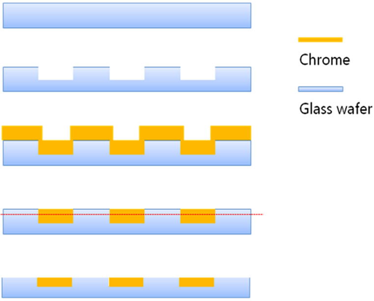
Figure 5. Planarization method using CMP.
planarization. In the present study, we used a hard pad, a general metal slurry, and a glass slurry for creating mechanical effects larger than the chemical effects in CMP. However, the chemical effect is not removed because of its importance in CMP [25]. Given that the slurry chemically affects the polishing quality, it was difficult to accurately predict the amount of etching. It is thus important to note that CMP does not exactly etch the metal as deeply as required. For example, an etching depth of exactly 1 μm may be desired. In reality, CMP results in an etching of 1 ± α μm where α is the CMP resolution, as depicted in Figure 6. The results vary, case-by-case, depending on the machine and the wafer. Thus, CMP tests are needed to obtain the correct error level. In this study, the error level was about 500 nm. This means that the actual etched depth is 1 ± 0.5 μm when the desired depth is 1μm.
The fabrication process is the well-known damascene method, (see Figure 5). The first step involves a deep etching of the wafer into the desired pattern. “Deep” here means that the depth is larger than the error level of the CMP. The next involves fully filling the etched grooves of the wafer with chrome. The final step is to polish the wafer using CMP until the top surface of the entire wafer appears. It is important that polishing is stopped before all of the electrode material is removed.
As a test sample, we used a 6 in. quartz glass wafer with a thickness of 0.7 mm and patterned it using a glass etcher and dry-etching equipment at 2 μm. Chrome was deposited to a depth of 2 μm using a sputter. At this point, the surface was opaque because the top was covered by 2 μm of chrome. We then etched the surface using CMP until the patterned surface of the glass wafer came into view. We used a commercial CMP machine (Labmaster). The pad and slurry for the planarization were IC1000 (Rohm and Haas) and Polypla (Fujimi), respectively. The
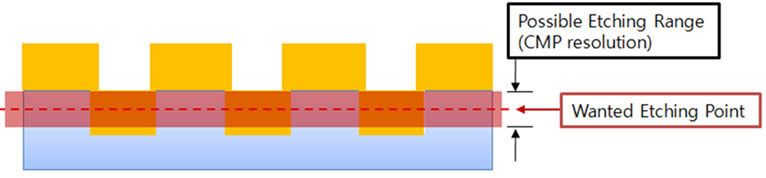
Figure 6. CMP resolution.
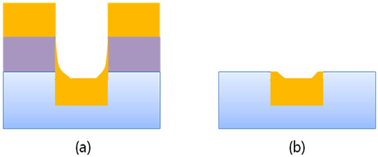
Figure 7. Problem with the lift-off process.
speed of CMP was approximately 80 RPM.
3.4. Common Processes of the Three Methods after Planarization
The fabrication process consisted of three common steps after planarization. The first step is a dicing process used to cut the fabricated wafer into devices. Dicing requires the use of ultraviolet (UV) tape or a PR to passivate the surface. However, some residue from the tape or PR may remain on the surface. These contaminants can be removed by acetone cleaning without attacking the chrome, although doing so is difficult after the final coating. Therefore, this cleaning step must immediately follow dicing. The second step is to deposit silane (SiH4) to create an adhesive layer between the diamond-like carbon (DLC) and the chrome. The deposition should be approximately 30 nm to provide the best adhesive force. The final step involves coating with DLC to a thickness of 200 nm.
4. Results
4.1. Evaluation of the Proposed Planarization Methods
Successful planarization could not be achieved using the lift-off process because of the difficulty of matching the thickness of the deposited electrode to the depth of the patterning. Although this is practically difficult, it is possible. Nevertheless, the reproducibility of this method is very low. Additionally, despite using an e-beam for deposition, the deposited electrode material attached to the PR sidewall. This is illustrated in Figure 7. The procedure left a residue at each edge of the electrode, increasing the surface roughness after cleaning by ultrasound and spinning. The problem of PR attaching to a sidewall can be solved by a special PR technique to enlarge the bottom space of the PR pattern after etching [13]. This special method uses a PR with an inclined wall (or multi-layered step) to enlarge the bottom space. The large space helps avoid the attachment of the metal at each boundary surface because the deposited electrode pattern size is smaller than the bottom space (Figure 8(a)). However, in case of the planarization method, the etched area is wider than the opened area of the upper surface of the PR because the etching method does not have high directionality (as in a beam); hence, it does not etch the target in the exact size of the opening (This is true for both wet etching and dry etching). Therefore, the special PR technique leaves some grooves after PR stripping in many cases, as seen in Figure 8(b). Consequently, it is ineffective to adapt this method to the sensor.
Figure 9 depicts a sample produced by the Etch-back
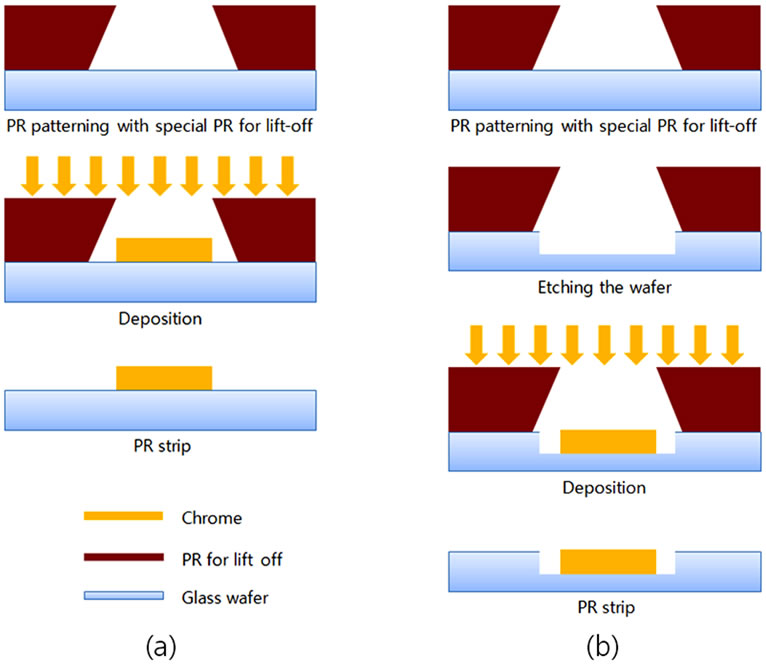
Figure 8. Lift-off method using PR. (a) General lift-off and (b) planarization using lift-off.
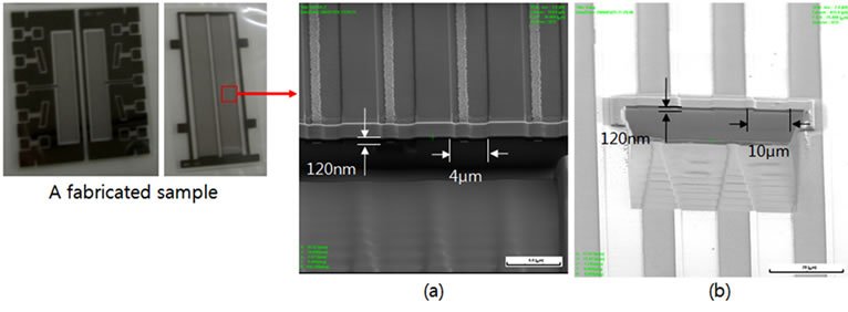
Figure 9. Results of etch-back. (a) Over-cut and (b) undercut.
process described in Section 3.2. The sectional view of the sample is obtained by a focused ion beam (FIB). As shown in Figure 9, the remaining electrode and the etched area of the glass differ in size, mainly because of a difference between the patterned depth and the deposited thickness and an alignment error. The alignment error is about 1 μm or more in most cases because most aligners use a manually operated optical microscope. Therefore, when the difference (between the depth and thickness) occurs due to an alignment error, it is difficult to determine when to stop etching because the electrode layer is deposited to cover the patterned boundary. This is the primary reason for overand under-cuts. In Figure 9(a), the remaining electrode pattern is smaller than the etched grooves in the wafer. This is an over-cut due to late termination of etching (over-etching), as previously described. On the other hand, Figure 9(b) shows an under-cut case caused by insufficient etching time. In practice, the etching rate is variable and non-linear; in addition, the alignment error and matching problem (between the deposited metal thickness and the etched depth on the substrate) are involved. Hence, it is difficult to stop at the right time (which is itself unclear). For these reasons, the etch-back method cannot be successfully adapted for planarization.
Figure 10 shows the result of planarization by CMP described in Section 3.3 for a sample with 10-μm-wide electrodes. The scanning electron microscopic image presented in Figure 10(a) was obtained using FIB, and the surface profile image presented in Figure 10(b) was measured by atomic force microscopy (AFM). Both images were obtained using same sample and similar surface area. The FIB image is approximately 70 μm by 80 μm and the AFM topography image is 80 μm by 80 μm area in which 4 electrodes can be covered. In the Figure 10(a), the electrode pattern and the glass can be found alternating at the same constant size. In the AFM topography which has 512 by 512 points (it means that one point is about 156 nm by 156 nm), the sample has height difference of about 15 nm with excluding some white points. However, it is difficult to separate the boundary between the electrode and the wafer in the AFM topography, even though the electrodes are formed well with 500 nm thickness. This means that the surface of the sample has no steps, even though the electrode has been patterned into the glass substrate. The result shows that CMP planarization was successful.
4.2. Application to CLECDiS
As described in the previous section, the CMP method was the only one that successfully planarized the surface. This method was subsequently applied to enhance the surface of CLECDiS [9,26,27], a contact-type displacement sensor. The sensor is fabricated by micromachining a glass wafer and chrome electrode. The glass wafer reduces the effect of the parasitic capacitor [28]. The chrome adheres well to the glass and is easy to deposit thickly. The coated layer of the contact device should not wear or
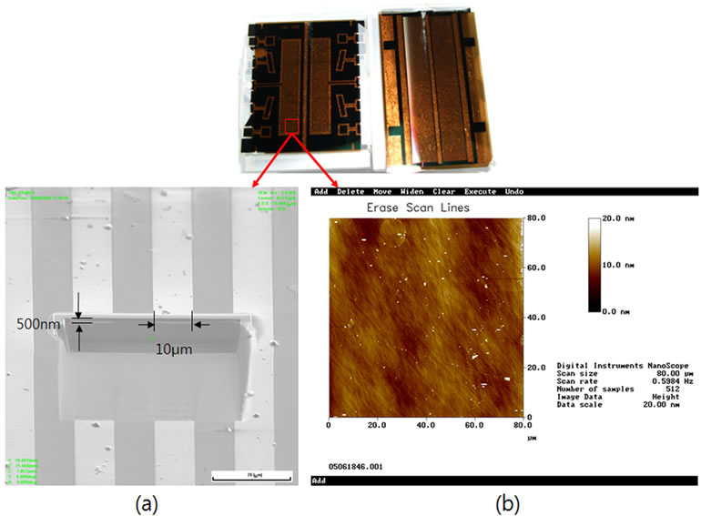
Figure 10. Results of CMP. (a) FIB image and AFM image.
deform easily. For this reason, we selected DLC (Diamond-like Carbon) for the layer, as it has a high hardness and a low friction coefficient [29-31]. However the DLCcoated sensor had a short lifespan, even though the coated surface showed no visible damage. To determine the reason for the short lifespan, a sectional view of the samples was observed (Figure 11). Figure 11(a) shows the surface profile of a sample before use, and Figure 11(b) shows a surface profile and a sectional view of a sample after use. Both surface profiles and sectional view were obtained by AFM, and FIB, respectively. Sharply deformed edges are seen at both corners of each pattern of the sample after use. The deformed edges are not found in samples before use or after use without contact. This suggests that the edges were sharply deformed during contact operation. If the contact surface is perfectly flat, it may be difficult to deform solely by friction. It is plausible that the deformation is caused by the electrode height and is linked to the collision problem (Section 2.1). In general, if collisions occur, an angled edge is formed and is usually rounded. However, although the top DLC surface has high hardness, the chrome layer under the coating layer is softer. Therefore, it is deformed instead of DLC. This deformation may cause edge deformation. If so, the lifespan should be longer when the sensor is planarized.
Figure 12 shows two signals. Figures 1(a) and 12(b) show the signals of a planarized sample using CMP and of a non-planarized sample, respectively. The samples were continuously used for approximately two hours per day. Although the non-planarized sample can only output a good signal for about seven days, the planarized sample can do so for over one month. As a result, the lifespan of the planarized sample is over four times longer
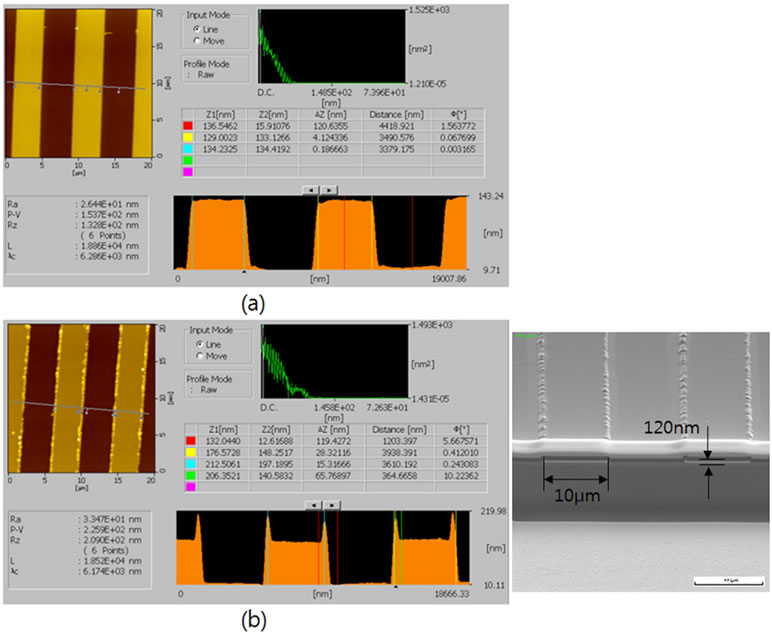
Figure 11. CLECDiS surface profiles. (a) Before use and (b) after use.
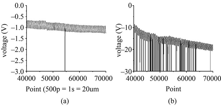
Figure 12. Two CLECDiS signals. (a) Planarized (30 day after starting operation) and (b) non-planarized (7 day after starting operation).
than that of the non-planarized sample. Although the lifespan of the planarized sample is still insufficient, this confirms our conjecture that the height difference is the problem.
5. Conclusions
In this study, we achieved improving life span in a high dynamic range contact-type capacitive displacement sensor by planarization. For this, we used the following planarization methods: lift-off, etch-back, and CMP. Although lift-off and etch-back are simple and low-cost methods, it was difficult to match the thickness of deposition to the patterned depth. In addition, the lift-off method has an associated problem with the PR in that it remains after stripping. The etch-back process involves an alignment error. The sample can be planarized, however, by CMP. Thus, CMP planarization was applied to CLECDiS. The lifespan of the sensor improved more than four times after planarization because of reduced collisions afforded by this process.
From these results, we suggested that planarization is required for contact devices and can improve their performance. The results confirmed our expectations and we achieved successfully improving performance of the sensor.
6. Acknowledgements
This work was supported by the National Research Foundation of Korea (NRF) grant funded by the Korea government (MEST) (No. 2011-0020435).
7. References
[1] S. Zhang and S. Kiyono, “An Absolute Calibration Method for Displacement Sensors,” Measurement, Vol. 29, 2001, pp. 11-20. doi:10.1016/S0263-2241(00)00023-3
[2] X. Li, “An Accurate Interface for Capacitive Sensors,” IEEE Transactions on Instrumentation and Measurement, Vol. 51, No. 5, 2002, pp. 935-939. doi:10.1109/TIM.2002.807793
[3] A. A. Kuijpers, G. J. M. Krijnen, R. J. Wiegerink, T. S. J. Lammerink and M. Elwenspoek, “A Micromachined Capacitive Incremental Position Sensor: Part 2. Experimental Assessment,” Journal of Micromechanics and Microengineering, Vol. 16, No. 6, 2006, pp. S125-S134. doi:10.1088/0960-1317/16/6/S19
[4] A. A. Arkadan, S. Subramaniam-Sivanesan and O. Douedari, “Design Optimization of a Capacitive Transducer for Displacement Measurement,” IEEE Transactions on Magnetics, Vol. 35, No. 3, 1999, pp. 1869-1872. doi:10.1109/20.767398
[5] F. Zhu and J. W. Spronck, “A Capacitive Tactile Sensor for Shear and Normal Force Measurements,” Sensors and Actuators A, Vol. 31, No. 1-3, 1992, pp. 115-120. doi:10.1016/0924-4247(92)80089-L
[6] F. Zhu and J. W. Spronck, “A Simple Capacitive Displacement Sensor,” Sensors and Actuators A, Vol. 25-27, 1991, pp. 265-269. doi:10.1016/0924-4247(91)87003-L
[7] W. C. Heerens, “Application of Capacitance Techniques in Sensor Design,” Journal of Physics E: Scientific Instruments, Vol. 19, 1986, pp. 897-906. doi:10.1088/0022-3735/19/11/002
[8] M. Hirasawa, M. Nakamura and M. Kanno, “Optimum Form of Capacitive Transducer for Displacement Measurement,” IEEE Transactions on Instrumentation and Measurement, Vol. IM-33, 1984, pp. 276-280. doi:10.1109/TIM.1984.4315224
[9] M. Kim, W. Moon, E. Yoon and K.-R. Lee, “A New Capacitive Displacement Sensor with High Accuracy and Long-Range,” Sensors and Actuators A, Vol. 103-131, 2006, pp. 135-141.
[10] M. Kim, W. Moon and W. Chung, “Capacitive Motor Sensor,” US Patent, US 6,996,495 B2. 2006, p.13.
[11] D. Kang, “Improvement Contact-Type Linear EncoderLike Capacitive Displacement Sensor (CLECDiS),” Engineering, Thesis of Master Degree, POSTECH, Pohang, 2006, p. 71.
[12] Wikipedia, the Free Encyclopedia, “Surface Roughness,” http://en.wikipedia.org/wiki/Surface_roughness
[13] I. Ishida, S. Tahara and Y. Wada, “Advanced Lift off Planarization Process for Josephson Integrated Circuits,” Applied Physics Letters, Vol. 53, 1988, pp. 316-318. doi:10.1063/1.99906
[14] Y. Ding, M. Pakala, P. Nguyen, H. Meng, Y. Huai and J. P. Wang, “Fabrication of Current-Induced Magnetization Switching Devices Using Etch-Back Planarization Process,” Journal of Applied Physics, Vol. 97, 2005, pp. 10C702-710C702-3.
[15] L. Wang, W. Zeng, W. Li and D. Sun, “Etch-Back in DDSOG Process by Ultrasonic Agitation and Application to Tunneling Gyroscope Fabrication,” Proceedings of the 4th IEEE International Conference on Nano/Micro Engineered and Moecular Systems, Shenzhen, China, 2009, pp. 156-159. doi:10.1109/NEMS.2009.5068548
[16] G. Grivna and R. Goodner, “A New Global Planarization Technique Using in Situ Isotropic Photoresist Mask Erosion,” Journal of Electrochemical Society, Vol. 141, 1994, pp. 251-254. doi:10.1149/1.2054693
[17] P. B. Zantye, A. Kumar and A. K. Sikder, “Chemical Mechanical Planarization for Microelectronics Applications,” Materials Science & Engineering R-Reports, Vol. 45, 2004, pp. 89-220. doi:10.1016/j.mser.2004.06.002
[18] S. Pandija, D. Roy and S. V. Babu, “Achievement of High Planarization Efficiency in CMP of Copper at a Reduced down Pressure,” Microelectronic Engineering, Vol. 86, No. 3, 2009, pp. 367-373. doi:10.1016/j.mee.2008.11.047
[19] Y. B. Park, J. H. Ahn, M. H. Lee, H. J. Kim and H. D. Jeong, “Removal Rate and Thermal Effect on Wafer Size in Cu CMP,” 2008 Autumn Conference, Korea Society of Precision Engineering, 2008, pp. 445-446.
[20] D. Rosales-Yeomans, D. De Nardis, L. Borucki and A. Philipossian, “Design and Evaluation of Pad Grooves for Copper CMP,” Journal of the Electrochemical Society, Vol. 155, No. 10, 2008, pp. H797-H806. doi:10.1149/1.2963268
[21] R. Ihnfeldt and J. B. Talbot, “The Effects of Copper CMP Slurry Chemistry on the Colloidal Behavior of Alumina Abrasives,” Journal of the Electrochemical Society, Vol. 153, No. 11, 2006, pp. G948-G955. doi:10.1149/1.2335982
[22] J.-B. Chiu, A.-J. Su, C.-C. Yu and S-H. Shen, “Planarization Strategy of Cu CMP,” Journal of the Electrochemical Society, Vol. 151, No. 4, 2004, pp. G217-G222. doi:10.1149/1.1649985
[23] J. C. Yang, D. W. Oh, G. W. Lee, C. L. Song and T. Kim, “Step Height Removal Mechanism of Chemical Mechanical Planarization (CMP) for Sub-Nano-Surface Finish,” Wear, 2009, Article in Press.
[24] A. R. Sethuraman, J. F. Wang and L. M. Cook, “Review of Planarization and Reliability Aspects of Future Interconnect Materials,” Journal of Electronic Materials, Vol. 25, No. 10, 1996, pp. 1617-1622. doi:10.1007/BF02655585
[25] H. Liang, “Chemical Boundary Lubrication in ChemicalMechanical Planarization,” Tribology International, Vol. 38, No. 3, 2005, pp. 235-242. doi:10.1016/j.triboint.2004.08.006
[26] M. Kim and W. Moon, “A New Linear Encoder-Like Capacitive Displacement Sensor,” Measurement, Vol. 39, No. 6, 2006, pp. 481-489. doi:10.1016/j.measurement.2005.12.012
[27] M. Kim and W. Moon, “A New Capacitive Displacement Sensor for High Accuracy and Long Range,” Journal of the Korean Sensors Society, Vol. 14, 2005, pp. 219-224.
[28] M. E. Kiziroglou, C. He and E. M. Yeatman, “NonResonant Electrostatic Energy Harvesting from a Rolling Mass,” 5th International Summer School and Symposium on Medical Devices and Biosensors (ISSS-MDBS), Hong Kong, 1-3 June 2008, pp. 318-321.
[29] J. L. Tech, “DLC (Diamond-Like Carbon),” J&L Tech, 2010. http://www.jnltech.co.kr/02technology/01.html
[30] K.-R. Lee and K. Y. Eun, “Diamond-Like Carbon Film,” Bulletin of The Korean Institute of Metals and Materials, Vol. 6, 1993, pp. 345-361.
[31] J. Robertson, “Properties of Diamond-Like Carbon,” Surface and Coatings Technology, Vol. 50, No. 3, 1992, pp. 185-203.