Journal of Sensor Technology
Vol.1 No.1(2011), Article ID:4330,8 pages DOI:10.4236/jst.2011.11002
Fabrication of Nanocrystalline TiO2 Thin Film Ammonia Vapor Sensor
*1Materials Research Laboratory, School of Physical Sciences, Solapur University, Solapur, India
2Crystal Technology Section, Bhabha Atomic Research Centre, Mumbai, India
3Department of Physics, Shivaji University, Kolhapur, India
E-mail: drvbpatil@gmail.com
Received February 9, 2011; revised March 1, 2011; accepted March 7, 2011
Keywords: Sol Gel Method, Structural Properties, Optical Properties, NH3 Sensor
Abstract
Nanocrystalline titanium oxide thin films have been deposited by spin coating technique and then have been analyzed to test their application in NH3 gas-sensing technology. In particular, spectrophotometric and conductivity measurements have been performed in order to determine the optical and electrical properties of titanium oxide thin films. The structure and the morphology of such material have been investigated by X ray diffraction, Scanning microscopy, high resolution electron microscopy and selected area electron diffraction. The X-ray diffraction measurements confirmed that the films grown by this technique have good crystalline tetragonal mixed anatase and rutile phase structure The HRTEM image of TiO2 thin film showed grains of about 50-60 nm in size with aggregation of 10-15 nm crystallites. Selected area electron diffraction pattern shows that the TiO2 films exhibited tetragonal structure. The surface morphology (SEM) of the TiO2 film showed that the nanoparticles are fine. The optical band gap of TiO2 film is 3.26 eV. Gas sensing properties showed that TiO2 films were sensitive as well as fast in responding to NH3. A high sensitivity for ammonia indicates that the TiO2 films are selective for this gas.
1. Introduction
It is well known that the electrical conductivities of semiconducting metal oxides change with the composition of the gas atmosphere surrounding them. For this reason metal oxides gained attention for potential application as sensing elements in gas detectors [1]. Between the metal oxides that undergo dramatic changes in their electrical conductivity owing to gas exposure the most analyzed were SnO2 [2-5], ZnO [6,7], WO3 [8,9] and V2O5 [10]. As with several metal oxides, titanium oxide is a polar material of technological importance since it is used as a substrate in catalytical and electrochemical processes [11]. These features make titanium oxide potentially suitable as gas sensing material [6].
Sensitivity, selectivity and stability are the most important characteristics of gas sensing materials. Indeed, an ideal sensor should respond to very low target gas concentrations, does not respond to other interfering gases, and has long term stability. Actually, optimum sensor performance is not often achieved due to an insufficient understanding of gas-film interactions and sensing mechanisms, and a lack of control on film parameters. For example the deposition parameters can affect the composition, the microstructure and the morphology of metal oxide films and, consequently, can have a strong influence on gas sensing properties.
To achieve a complete control on films structure and so to develop a new generation of chemical sensors, on one hand there is a need to improve the material processing and on the other to perform a careful analysis of both structural and physical properties of the material.
In the present study nanocrystalline titanium oxide films have been deposited by spin coating technique. In particular, X-ray diffraction, high resolution transmission electron microscopy observations, together with spectrophotometric and conductivity measurements, have been considered in order to determine both the microstructure and the optical and electrical properties as a NH3 gas sensor annealed at 700oC.
2. Experimental Details
Nanocrystalline TiO2 thin films are synthesized by a sol-gel method using titanium isopropoxide as a source of titanium. In a typical experiment; 3.7 ml of titanium isopropoxide was added to 40 ml of methanol and stirred vigorously at 60oC for 1 hr, leading to the formation of white powder. The powder was sintered at various temperatures ranging from 400-700oC with a fixed annealing time of 1hr in air to obtain TiO2 films with different crystallite sizes. The nanocrystalline TiO2 powder was further dissolved in mcresol. The solution was stirred for 1 hr at room temperature and filtered. This solution was deposited on to a glass substrate by a single wafer spin processor (APEX Instruments, Kolkata, Model SCU 2007). After setting the substrate on the disk of the spin coater, the coating solution (approximately 0.2 ml) was dropped and spin-coated at 3000 RPM for 40 s in air and dried on a hot plate at 100oC for 10 min.
The structural properties of the films were investigated by X-ray diffraction (XRD) (Philips PW-3710, Holland) using filtered CuKα radiation (l= 1.5406 A0 ). High resolution transmission electron microscopy (HRTEM) and selected area electron diffraction (SAED) pattern were obtained in order to investigate the morphology and structure of titanium oxide thin films. The HRTEM images were recorded with a Hitachi Model H-800 transmission electron microscope. In order to determine the particle size and morphology, the sintered powder was dispersed in mcresol and ultrasonicated using Microclean-103 (OSCAR ultrasonic bath apparatus) to separate out individual particles. The size and morphology of the thin films were then observed on SEM Model: JEOL JSM 6360 at 20 kV. The optical absorption spectra of the TiO2 thin films were measured using a double-beam spectrophotometer Shimadzu UV-140 over 200-1000 nm wavelength range. The thickness (100-200 nm).of the film was measured by using Dektak profilometer.
For gas sensitivity measurement TiO2 sensors were prepared by spin coating on the glass substrate. Electrodes on the film were deposited by thermal evaporation of gold in a high vacuum system (2.5*10e-5), by masking the film with the help of Al foil (0.5mm width and length is according to substrate). For taking electrical connection two Ag wires were stick on gold pads using Ag paste. The resistance was measured using Rigol 6½ digit DMM. For monitoring the response of the films to various gases, the films were mounted in 250cc air tight container and the known gas (NH3, H2S, C2H5OH, CH3OH and NO2) of particular concentration was injected through a syringe. All the gas sensitivity measurements were carried out at operating temperature 200oC.
3. Results and Discussion
The sintering temperature was varied between 400- 700oC and the samples are denoted as Ti400, Ti500 Ti600 and Ti700 respectively.
3.1. Structural Properties
Figure 1 shows the X-ray diffraction patterns of all nanocrystalline TiO2 samples. The X-ray spectra exhibit the well-defined diffraction peaks, demonstrating that the samples are polycrystalline. The samples sintered at 400oC and 500oC are relatively less crystalline in nature while the dramatic improvement in the crystallinity with the prominent (101) peak along with (103), (112), (200), (105), (211), (213) and (220) reflection of the anatase TiO2 phase is observed when the samples sintered at 600oC and a mixed anatase and rutile phase is obtained for sample sintered at 700oC (Ti700). The crystallites are randomly oriented and the d-values calculated for the diffraction peaks are in good agreement with those given in JCPDS data cards (JCPDS No.78-2485 and 78-2486) for TiO2 anatase and rutile phase. This means that TiO2 has been crystallized in a tetragonal mixed anatase and rutile form. These results are in good agreement with other reports on the mixed phase TiO2 by sol gel method [5-8]. The lattice constants calculated from the present data are a = 3.7837 Å and c = 9.5087 Å respectively. From Figure 1 it is observed that the peak along (101) plane is dominant and its (anatase phase) intensity increased with the sintering temperature. However, its full width at half-maxima FWHM doesn’t change appreciably [9,10]. The grain size of all the TiO2 samples was calculated using Scherer’s equation and it is in the range of 50-60 nm, revealing a fine nanocrystalline grain structure.
3.2 Microstructural and Morphological Properties
AFM (non contact mode) was used to record the topography of the Ti700 sample. In this mode, the tip of the cantilever does not contact with the sample surface. The cantilever is instead oscillated at a frequency slightly above its resonance frequency where the amplitude of oscillation is typically a few nanometers (<10 nm). The surface morphologies of the TiO2 nanoparticles exhibit notable features. Figure 2 shows 2D and 3D AFM images (3 μm × 3 μm) of the Ti700 sample. The average particle size of TiO2 is found to be in the range of 50-60 nm with surface roughness of about 7-19 nm.
Figure 3(a) shows high resolution TEM image of Ti700 sample recorded from typical regions of the film. The HRTEM image shows a large number of crystalline grains appeared in a structured matrix and the nanocrystallites have a diameter in the range of 2-3 nm which
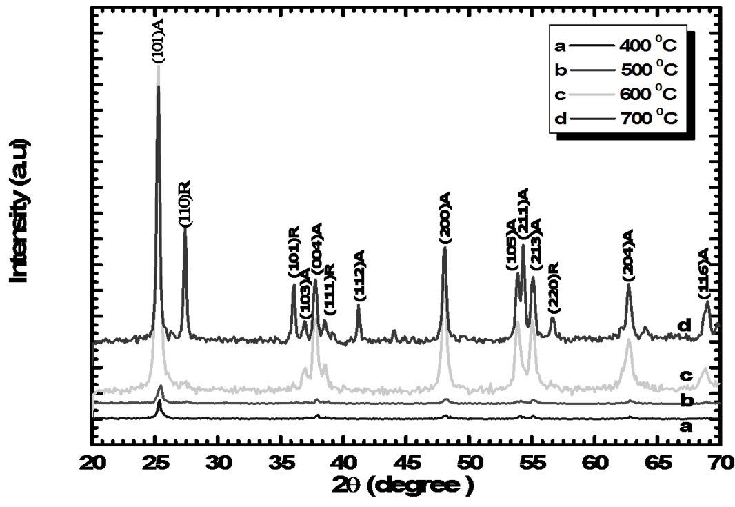
Figure 1. X ray diffraction patterns of TiO2 film at different sintering temperatures: a) Ti 400oC, b) Ti 500oC, c) Ti 600oC and d) Ti 700oC for 1 hr in air.

Figure 2. AFM images of TiO2 thin films sintered at 700oC for 1 hr in air. a) Planer view; b) 3D view.
exhibits lattice spacing’s of about 0.16 nm. This agrees well with the literature [5-8]. Figure 3(b) shows the diffraction patterns obtained from Ti700 sample. The different arrangement of dominant diffracted rings indicates a phase evolution of crystalline grains as a consequence of thermal annealing.
Figure 4 shows the SEM micrographs of the entire TiO2 thin films (Ti400-Ti700).
For Ti400 sample, the powder was sintered at 400oC, before it was spin coated. It is observed that at 400oC, the particles of different shapes and sizes are formed due to insufficient temperature for its homogenation.When the powder sintered at 500oC and 600oC, larger crystallites are broken down to a smaller one. This causes relatively better homogeneity. The finely divided nanocrystalline monodisperesed nanoparticles of TiO2 are observed at 700oC.
3.3. Optical Properties
The optical constants namely absorption coefficient (α), energy gap (Eg) and the type of the optical transition have been determined by examining an optical absorption spectrum over 200-1000 nm of all the TiO2 films. Figure 5 shows plots of (αhν)2 as a function of photon energy (hν) for TiO2 thin films deposited onto glass substrates as a function annealing temperature (400-700oC). The optical absorption data were analyzed using the fol
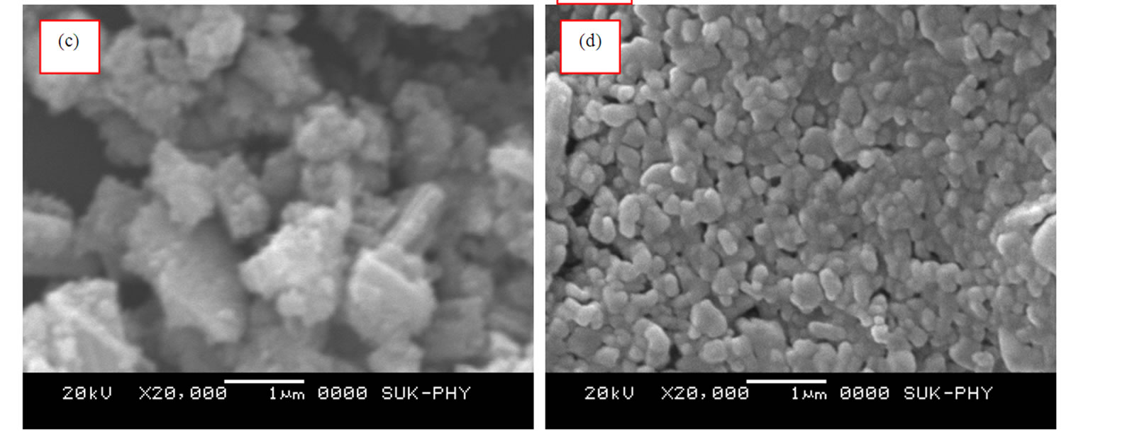

Figure 3. HRTEM of TiO2 thin film sintered at 700oC for 1 hr in air. a) microstructure; b) Selected Area Electron Diffraction pattern.

Figure 4. SEM image of TiO2 thin film at different sintering temperatures: a) Ti 400oC b) Ti 500oC, c) Ti 600oC and d) Ti 700oC for 1 hr in air.
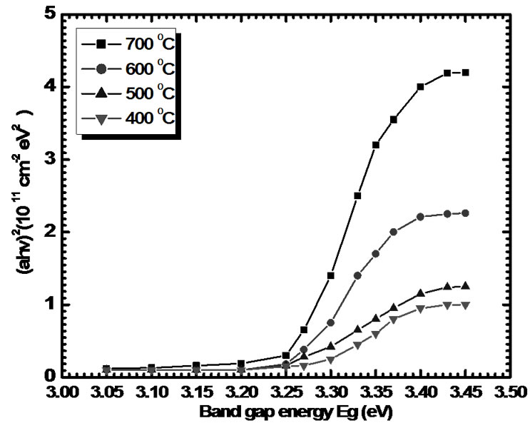
Figure 5. Plot of (αhυ)2 versus (hυ) for different sintering temperatures for 1 hr in air.
lowing classical relation for near edge optical absorption in semiconductor.
α = α0 (hν-Eg)n/hν (1)
The values of the optical band gap decrease slightly with increasing annealing temperature (400-700oC). The decrease in band gap indicates an improvement of the quality of the film due to the annealing out of the structural defects. This is in agreement with the experimental results of XRD analysis. According to XRD results, the mean grain size increased with increased annealing temperature. As grain size increased, the grain boundary density of a film decreased, subsequently, the scattering of carriers at grain boundaries decreased [12]. A continuous increase of optical constants and also a shift in absorption edge to a higher wavelength with increasing annealing temperature may be attributed to the improvement in the crystalline quality of the films along with reduction in porosity. It is also found that the optical absorption coefficient is larger for all the films (≈ 10 4cm-1). This may be accounted for the fact that the quality of the TiO2 film improves when the sample is annealed at a higher temperature (in this case 700 oC). The (αhυ)2 versus hυ plots show straight line behaviour on the higher energy side indicating a direct type of transitions involved in these films. The type of transitions for TiO2 films sintered at 400-700oC was confirmed by plotting ln(αhυ) versus ln(hυ-Eg) variation [12,13].
3.4. Gas sensitivity Measurements
The gas sensitivity of a film is usually measured as the percentage change in film resistance on gas exposure, or may be defined as the ratio of its resistance in air to its steady state value in the presence of a gas, or vice versa. Irrespective of the definition one uses, it is important to monitor the (change in) electrical resistance of a sensor film. Here, we describe the operation of our sensor films at operating temperature 200oC.
For measurement of change in resistance on exposure to gases, the sensor head was put in an air-tight chamber of volume 250 ml, a pre-defined concentration of gas taken from calibrated cannister of 100 ppm was introduced in this chamber by syringe (Figure 6). The resistance of the film was measured before and after exposure to gas.
Gas sensitivity = Ra/Rg (2)
where Ra is the resistance in air and Rg is the resistance in a sample gas.
It is observed that a TiO2 thin film at 700oC provides the TiO2 particles with the desired tetragonal crystal structure and nanocrystalline TiO2 particles. These studies have revealed that the TiO2 thin films at 700oC may provide improved gas sensing properties and therefore the present paper aims at the gas sensing properties of TiO2 thin films at 700oC.
Figure 7 shows the sensitivity of titanium oxide films to 100 ppm of ammonia gas as a function of working temperature. As evident, the sensitivity increases with the temperature and reaches a maximum value in correspondence of T = 200°C. If the temperature increases again, the sensitivity decreases. This behavior can be explained in analogy with the mechanism of gas adsorption and desorption on SnO2, [14] ZnO [15] and ITO [16] films. An n-type metal-oxide can adsorb oxygen from the atmosphere both in the O2− and in the O− species. The adsorption of O− is the most interesting process in sensors, because this oxygen ion is the more reactive and thus makes the material more sensitive to the presence of reducing agents, in our case NH3.
Now, at relatively low temperature the surface preferentially adsorbs O2− and the sensitivity of the material is consequently very small. As the temperature increases, the dominant process becomes the adsorption of O−, then the sensitivity of the material increases too. If the temperature increases too much, progressive desorption of all oxygen ionic species previously adsorbed occurs and the sensitivity decreases.
The gas sensing properties of TiO2 film was carried out for NH3, CH3OH, C2H5OH, H2S and NO2 gases. All the measurements were carried out at operating temperature 200oC. To determine response and recovery times, a film was exposed to 100 ppm concentrations of CH3OH, C2H5OH, NO2, H2S, and NH3 and its resistance was recorded as a function of time. The response time has been defined as the time taken to attain 90% of final value, and the recovery time as the time taken to regain 10% of the base value. It was observed that the resistance of the TiO2 films decreases on exposure to H2S, NH3
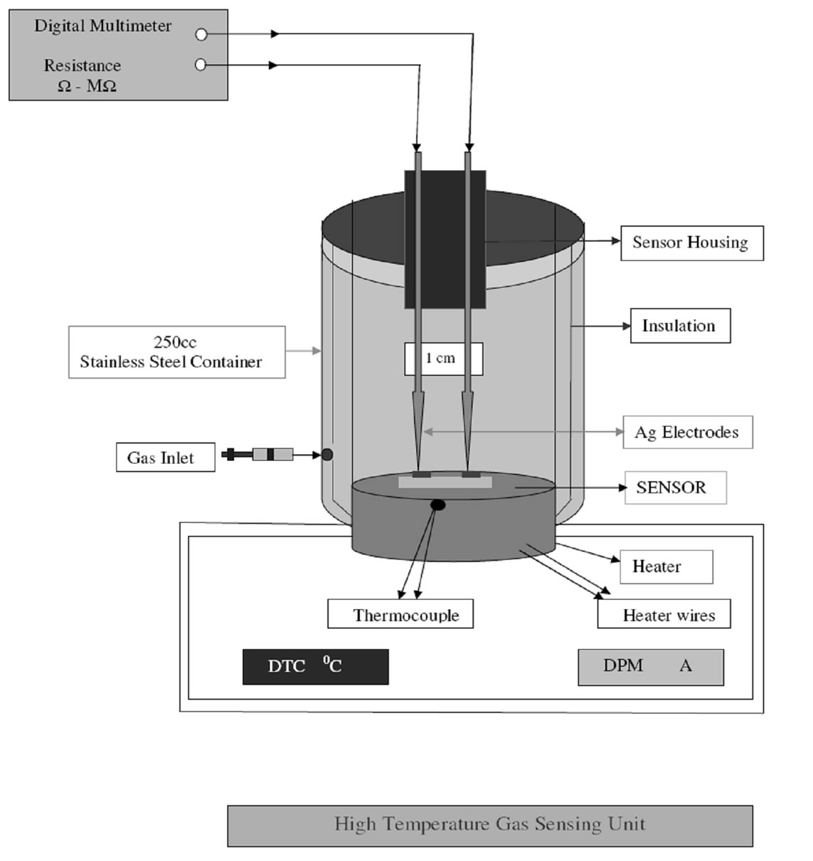
Figure 6. High temperature gas sensor unit.
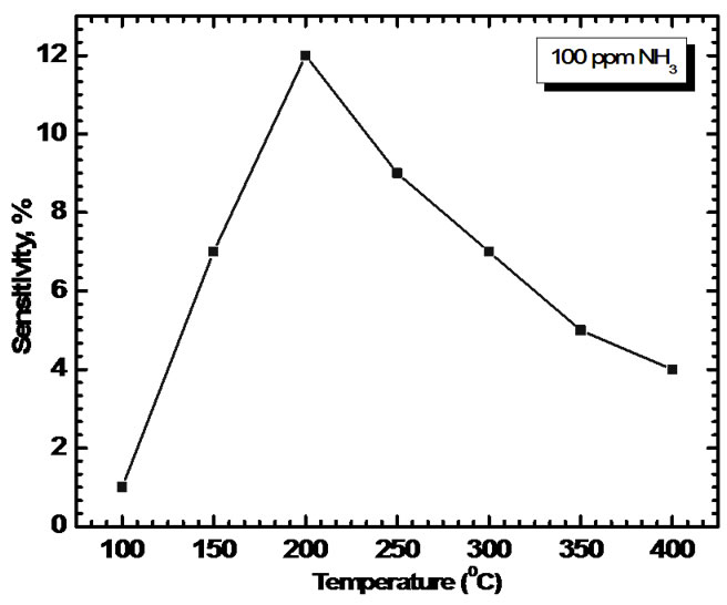
Figure 7. Sensitivity of TiO2 films to 100 ppm of ammonia gas as a function of working temperature.
CH3OH andC2H5OH gas where as it increases on exposure to and NO2 gas.
Typical gas response curves of TiO2 films for 20-100 ppm concentrations of NH3, is shown in Figure 8.
The sensitivity is defined as:
Sensitivity (%) = │ (Rgas- Rair)/Rair│ X 100 (3)
An attempt was made to study selectivity of TiO2 films for 100 ppm concentration of NH3 as compared to the sensitivities of CH3-OH, C2H5-OH, NO2 and H2S. The bar chart for selectivity is as shown in Figure 9. It is observed that TiO2 thin films can sense NH3 with higher sensitivity value as compared to other gases. It is observed that TiO2 film is sensitive as well as fast in responding to NH3. The response for NH3 is better by a factor of ~ 11 and also faster than other gases. A high sensitivity for ammonia indicates that the TiO2 films are selective for this gas.
The higher sensitivity towards NH3 than CH3OH, C2H5OH, NO2 and H2S, can be explained on the basis of different interactions between sensing film and adsorbed gas. TiO2 is n-type materials and when it interacts with reducing gas such as NH3, CH3OH, C2H5OH and H2S there is increase in charge carrier density. This results in increasing the conductivity of material and film resis-
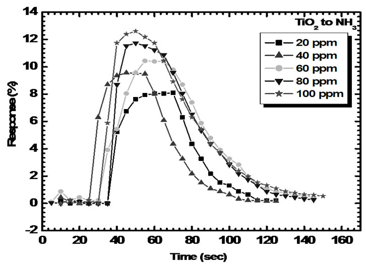
Figure 8 .Response curve of TiO2 films for 100 ppm NH3 in at the optimum working temperature.
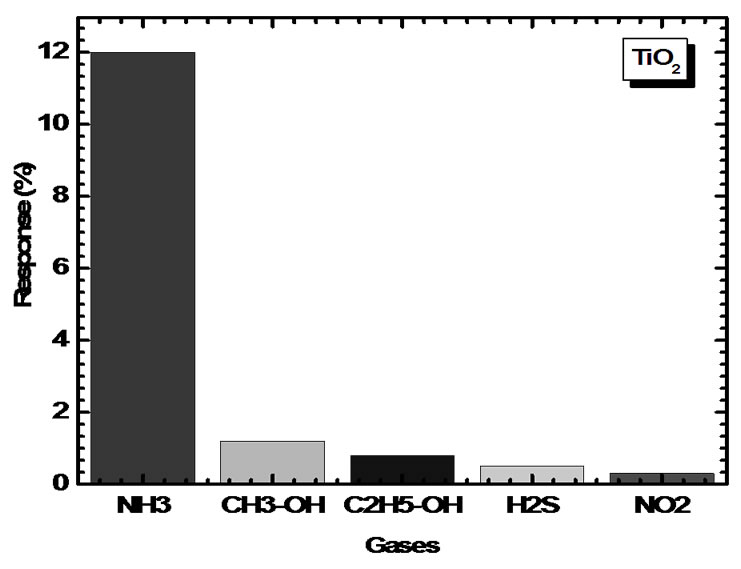
Figure 9. Gas responses of TiO2 sensor film to 100 ppm of NH3, CH3-OH, C2H5-OH, NO2, H2S and NO2.
tance decreases. In case of oxidizing gas like NO2 there is a decrease in charge carrier concentration and thereby decreasing conductivity. The interaction of H2S, CH3OH, C2H5OH and NO2 with TiO2 film is very less as compared to NH3, hence it shows very slow response and less sensitivity. The response values of TiO2 sensor film is plotted as a function of NH3 concentration in Figure 10. It is observed that the response slows down at higher concentration; this may be due to less availability of surface area with possible reaction sites on surface of the film.
Figure 11 shows electrical response of TiO2 to 20, 40, 60, 80 and 100 ppm of NH3. As seen from fig. the resistance of sensor film decreases dramatically upon exposure to ammonia vapor, attains stable value and increases gradually after being transferred to clean air.
4. Conclusions
In this paper we have reported on the preparation of tita-
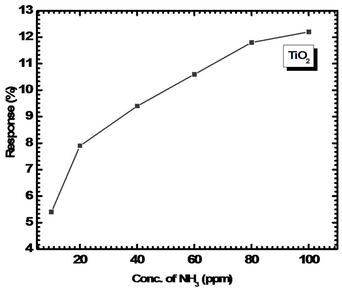
Figure 10. Response of TiO2 thin film sensor to NH3 (10- 100 ppm).
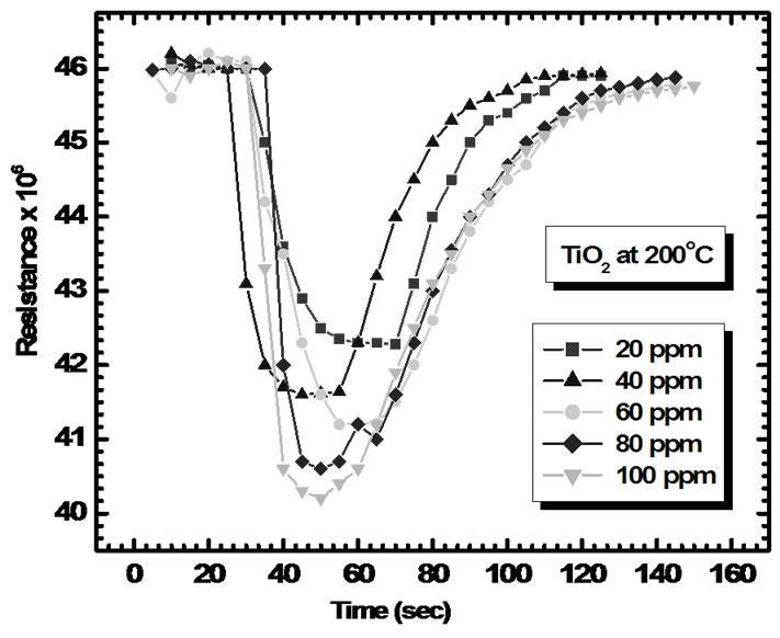
Figure 11. Gas responses of TiO2 sensor film to 20-100 ppm of NH3.
nium oxide thin films and on subsequent microstructural and physical characterizations. High resolution Transmission electron microscopy observation evidenced compositional and structural modification induced by thermal annealing. A strict relationship between structural and electrical properties can be observed by a comparison of structural analysis results and electrical characterization. The XRD results reveal that the deposited thin film of TiO2 has a good nanocrystalline tetragonal mixed anatase and rutile phase structure. The AFM, HRTEM, and SEM results demonstrate that a uniform surface morphology and the nanoparticles are fine with an average grain size of about 50-60 nm. Optical studies showed that the TiO2 has high absorption coefficient (≈ 104 cm-1) with a direct band gap. The optical band gap decreases slightly with increasing sintering temperature (3.26-3.24 eV).
As regards the gas sensing properties of titanium oxide films, we can conclude that they are promising sensors of NH3 in air, with a negligible response to H2S NO, CH3OH and C2H5OH gases.
5. Acknowledgments
Authors (VBP) are grateful to DAE-BRNS, for financial support through the scheme no.2010/37P/45/BRNS/ 1442.
6. References
[1] H. Meixner and U. Lampe, “Metal Oxide Sensors,” Sensors and Actuators B: Chemical, Vol. 33, No. 1-3, July 1996, pp. 198-202. doi:10.1016/0925-4005(96)80098-0
[2] T. Oyabu, “Sensing characteristics of SnO2 thin film gas sensor,” Journal of Applied Physics, Vol. 53, No. 4, April 1982, pp.2785-89. doi:10.1063/1.331079
[3] J. F. Mc Aleer, P. T. Moseley, J. O. W. Norris, D. E. Williams, P. Taylor and B. C. Tofield, “Tin Oxide Based Gas Sensors,” Materials Chemistry and Physics, Vol. 17, No. 6, 1987, pp. 577-583. doi:10.1016/0254-0584(87)90017-4
[4] M. Di Giulio, G. Micocci, A. Serra, A. Tepore, R. Rella and P. Siciliano, “SnO2 Thin Films for Gas Sensor Prepared by r.f. Reactive Sputtering,” Sensors and Actuators B: Chemical ,Vol. 25, No. 1-3, April 1995, pp. 465-468. doi:10.1016/0925-4005(94)01397-7
[5] M. Di Giulio, G. Micocci, A. Serra, A. Tepore, R. Rella and P. Siciliano, “Characteristics of Reactively Sputtered Pt–SnO2 Thin Films for CO Gas Sensors,” Journal of Vacuum Science & Technology A: Vacuum, Surfaces, and Films, Vol. 14, No. 4, June 1996, pp. 2215-2220. doi:10.1116/1.580049
[6] F. Boccuzzi, E. Guglielmetti, and A. Chiorino, “IR Study of Gas-Sensor Materials: NO Interaction on ZnO and TiO2, Pure or Modified by Metals,” Sensors and Actuators B: Chemical, Vol. 7, No 1-3, March 1992, pp. 645- 650. doi:10.1016/0925-4005(92)80379-C
[7] B. Bott, T. A. Jones and B. Mann, “The detection and measurement of CO using ZnO single Crystals,” Sensors and Actuators, Vol. 5, No. 1, January 1984, pp. 65-73. doi:10.1016/0250-6874(84)87007-9
[8] H. M. Lin, C. M. Hsu, H. Y. Yang, P. Y. Lee and C. C. Yang, “Nanocrystalline WO3-Based H2S Sensors,” Sensors and Actuators B: Chemical Vol. 22, No. 1, October 1994, pp. 63-68. doi:10.1016/0925-4005(94)01256-3
[9] M. Cantalini, H. T. Sun, M. Faccio, M. Pelino, S. Santucci, L. Lozzi and M. Passacantando, “NO2 Sensitivity of WO3 Thin Film Obtained by High Vacuum Thermal Evaporation,” Sensors and Actuators B: Chemical, Vol. 31, No. 1-2, February 1996, pp. 81-87. doi:10.1016/0925-4005(96)80020-7
[10] O. Schillin and K. Colbow, “A Mechanism for Sensing Reducing Gases with Vanadium Pentoxide Films,” Sensors and Actuators B: Chemical, Vol. 21, No. 2, August 1994, pp. 151-157. doi:10.1016/0925-4005(94)80017-0
[11] K. M. Glaassford, N. Troullier, J. L. Martins and J. R. Chelikowsky, “Electronic and Structural Properties of TiO2 in the Rutile Structure,” Solid State Communications, Vol. 76, No. 5, November 1990, pp. 635-638. doi:10.1016/0038-1098(90)90105-K
[12] K. B. Sundaram and A. Khan, “High Quality Zinc Oxide Films by Pulsed Laser Ablation,” Thin Solid Films, Vol. 295, No 1-2, February 1997, pp. 104-106. doi:10.1016/S0040-6090(96)09274-7
[13] J. Aranovich, A. Ortiz and R. H. Bube, “Properties of Zinc Oxide Films Prepared by the Oxidation of Diethyl Zinc,” Journal of Applied Physics, Vol. 52, No, 11, 1981, pp. 6685-6693. doi:10.1116/1.570167
[14] M. N. Islam, M. O. Hakim and H. Rahman, “Interaction of Tin Oxide Surface with O2, H2O and H2,” Surface Science, Vol. 86, 1979, pp. 335-344. doi:10.1007/BF01233137
[15] S. Major and K. L. Chopra, “Hall Effect Studies of Oxygen Chemisorption on Zinc Oxide,” Journal of Catalysis, Vol. 14, No. 3, July 1969, pp. 257-260. doi:10.1016/0165-1633(88)90014-7
[16] M. de la L. Olvera, A. Maldonado, R. Asomoza, M. Konagai and M. Asomoza, “Reactively Sputtered Indium tin Oxide Polycrystalline Thin Films as NO and NO2 Gas Sensors,” Thin Solid Films, Vol. 186, No. 2, May 1990, pp. 349-360. doi:10.1016/0040-6090(93)90364-U