Crystal Structure Theory and Applications
Vol.3 No.1(2014), Article ID:43964,12 pages DOI:10.4236/csta.2014.31002
Band Gap Effects in a Two-Dimensional Regular Polygonal Graphene-Like Structure
Zi-Gui Huang*, Chun-Fu Su
Department of Mechanical Design Engineering, National Formosa University, Taiwan
Email: *zghuang0119@nfu.edu.tw
Copyright © 2014 by authors and Scientific Research Publishing Inc.
This work is licensed under the Creative Commons Attribution International License (CC BY).
http://creativecommons.org/licenses/by/4.0/


Received 12 January 2014; revised 11 February 2014; accepted 5 March 2014
ABSTRACT
This study proposes a novel phononic-crystal acoustic wave device (AWD). A graphene atomic structure was adopted as the main research subject, and a graphene-like structure was designed using piezoelectric material ZnO and its periodic boundary conditions were defined using the finite element method (FEM). The study conducts acoustic-wave propagation analysis in the frequency domain on the 2D graphene-like structure according to Bloch theory to understand the band gap effects generated by its natural vibration. The effects of shape transformation from a hexagonal honeycomb structure into a regular polygon were also investigated regarding the band gap phenomenon. Thus, this study compared and analyzed numerous 2D polygonal graphene-like structures with a fixed bond diameter (d = 2R = 0.7 mm), bonding stick width (0.2 mm), and side length (1 mm), and observed the trends of the band gap changes under natural vibration for designing an optimal AWD; the studied 2D polygonal models were a square, and a regular hexagon, octagon, and decagon.
Keywords:Phononic Crystal; Band Gap; Finite Element Method

1. Introduction
The development of nanomaterials has flourished over recent decades, and the most popular research subject is graphene. Graphene is a flat monolayer film with a hexagonal honeycomb shape consisting of carbon atoms. Graphene was considered to be a hypothetical structure that could not exist independently until 2004, when two physicists from the University of Manchester, Andre Geim and Konstantin Novoselov, used the method of peeling with Scotch tape and obtained a 1-atom-thick graphene film [1] [2] . Under conditions of low light transmittance and low electrical resistance, the electron mobility of graphene is greater than that of silicon crystal; therefore, graphene can be employed to develop thinner electronic components and photonic devices with high conductivity [3] -[16] .
The development of photonic crystals has advanced yearly [17] -[20] . Considering the analogous fluctuation characteristics of photons and phonons, different material compositions or periodic structures obtained from changes in shape can be used to develop new acoustic wave devices (AWDs) or acoustic wave filters if the elastic waves that pass through also generate a band gap after appropriately adjusting the material parameters of these periodic structures. Sigalas et al. [21] and Kushwaha et al. [22] proposed the concept of phononic crystals and theoretically confirmed that during predictions of acoustic wave propagation, a complete band gap could be identified within elastic media in a 2D periodic array. A complete band gap implies that phononic crystals are capable of completely blocking certain frequencies from passing through the structure [23] -[27] .
This study focused on the graphene structure, which possesses the most potential for development, and created a hypothetic graphene-like structural design. The periodic boundary was defined by 2D finite element method (FEM) and the vibration behavior of the structure was analyzed. This study also investigated the role of ZnO in the band gap and the trends of the dispersion curve in the graphene-like periodic structure by assuming that the graphene-like structure was a square, and a regular hexagon, octagon, and decagon.
2. Design and Planning of a 2D Graphene-Like Structure
COMSOL Multiphysics, a finite element analysis software program, was used to analyze the vibration and numerical construction of the 2D graphene-like structure. Figure 1 shows the distribution of the 2D graphene-like structure. The primitive unit cell of the 2D graphene-like structure has a hexagonal structure and is composed of ZnO piezoelectric material. Once a driving voltage is supplied, the piezoelectric effect that converts mechanical and electrical energy is generated; because of periodic propagation characteristics, the energy is infinitely propagated between the two materials. Consequently, a graphene-like structure could generate frequency vibrations through the piezoelectric effect.
The model discussed in this study is a 2D graphene-like structure. An X-Y 2D planar drawing of the graphene-like structure was created based on the actual distribution of the monolayer graphene structure to observe the conditions of the band gap effect. This study designed four types of 2D graphene-like structures with varying numbers of sides: a square, and a regular hexagon, octagon, and decagon; the side length of all polygons was 1 mm. The band gap phenomenon is influenced by changes in the basic structural conditions of the graphene-like structure, which include the bond diameter (d = 2R), bond width, and the equilateral length. Figure 2(b) shows a schematic diagram of the size of a hexagonal primitive unit cell; the length is 1.73 mm, the width is 3 mm, the bond radius is R = 0.35 mm, the width of the bonding stick is 0.2 mm, and the length of the hexagonal side is 1 mm. Figure 2(a) shows a schematic diagram of a square mesh structure; the length and the width are both 1 mm. Figure 2(c) presents a regular octagonal mesh structure with a length of 2.41 and width of 3.41 mm. Figure 2(d) indicates a regular decagonal mesh structure with a length of 3.08 and width of 4.23 mm. Each of the regular polygonal mesh structures is designed based on a standardized construction scale with a fixed bond diameter (d = 2R = 0.7 mm), a bond width of 0.2 mm, and an equilateral length of 1 mm.
An ideal phononic crystal has translational periodicity and spatial symmetry. Using Bloch theory, the periodic structure can be simplified and the boundary conditions can be defined using the FEM to incorporate a simplified primitive unit cell into the periodic boundary conditions of displacement and stress for periodic system analysis:
 . (1)
. (1)
 . (2)
. (2)
where k is a wave vector,  is the stress field, and
  and
and  are periodic functions that fulfill the following relations [28] .
 . (3)
. (3)
 . (4)
. (4)
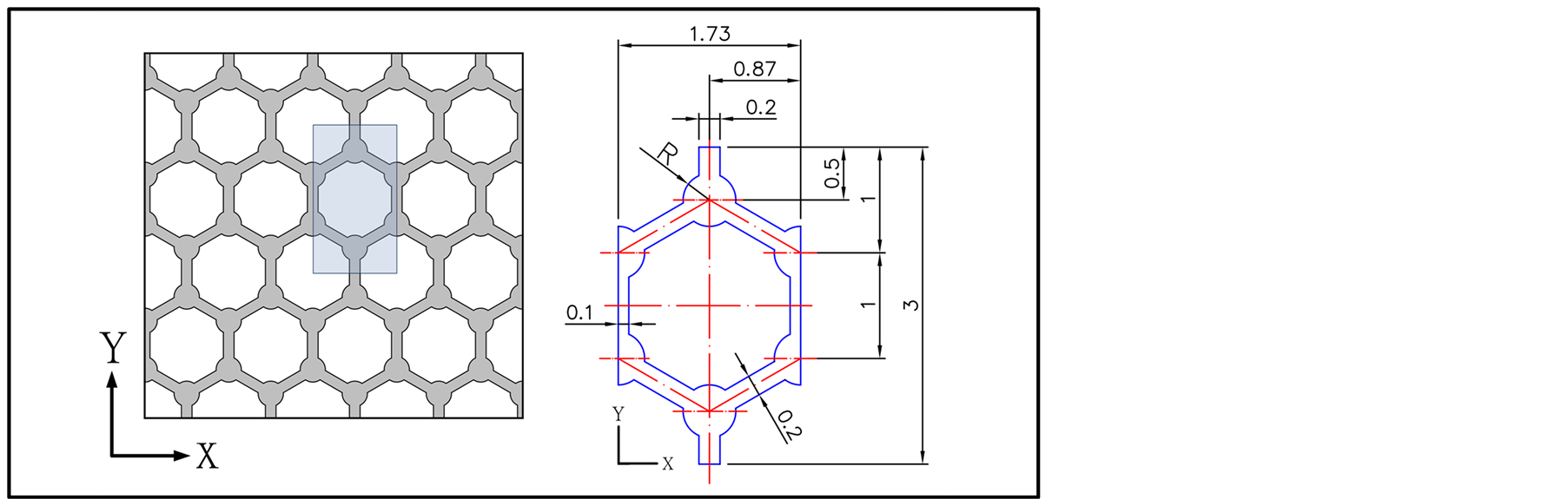
Figure 1. The schematic distribution of the 2D graphene-like structure.
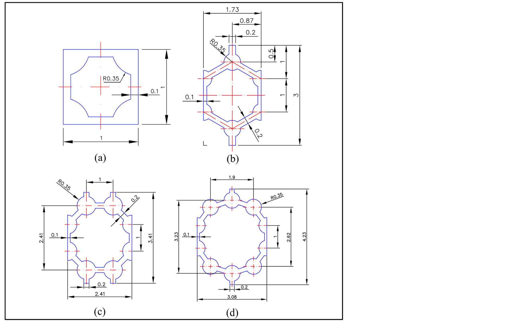
Figure 2. Schematic diagram of each periodic graphene-like structure. (a) the size of the square graphene-like structure; (b) the size of the regular hexagonal graphene-like structure; (c) the size of the regular octagonal graphene-like structure; (d) the size of the regular decagonal graphene-like structure.
From (3) and (4), the displacement and stress functions indicate translational periodicity. Therefore, phononic crystals with periodic structures can be further simplified into primitive unit cells to compute the eigenfrequency of any wave vector.
The key to examining phononic crystals is identifying the band gap. To accurately analyze the band frequency value in the band gap and the corresponding degree of deformation in the vibration mode, the element size (i.e., the mesh size) cannot be smaller than the standard number, or an irregular vibration mode is generated and the resonance mode is neglected. Therefore, element convergence analysis was conducted based on the regular hexagonal structure. As shown in Figure 3, the modal frequency error is lower than 0.02% with 9666 finite elements and a corresponding element size of 2.47 × 10⁻⁵ mm. Although convergence occurs at a slower rate, the required modal band and the range of the band gap can stably converge. Thus, the elements of a regular hexagon were used as a reference to adjust the elements of the other three polygons. Table 1 shows that the element size of a square is 1.2 × 10⁻⁵ mm and the number of corresponding elements is 9782. The element size

Figure 3. The mesh convergence trend of the regular hexagonal graphene-like structure.

Table 1. The element numbers in regular polygons.
of a regular octagon is 2.8 × 10⁻⁵ mm and the number of corresponding elements is 11,376. The element size of a regular decagon is 2.7 × 10⁻⁵ mm and the number of corresponding elements is 15,385.
3. Analysis Using Finite Element Software
The use of ZnO in 2D graphene-like structures provides a significant band gap phenomenon. In addition, using ZnO is feasible and inexpensive in the current production processes, and doping is likely to occur when ZnO is used in conductive films. Therefore, a new AWD is developed through finite element analysis. The focus of this study was to investigate the natural vibration phenomenon of polygonal graphene-like structures in a 2D X-Y mode.
3.1. Analysis Results
The number of finite elements determines the simulation outcomes. According to the test results shown in Section II, the frequency range for the band gap of the four phononic crystalline structures in this study was between 0 and 7 MHz. Figures 4 to 7 show the dispersion relationship of each regular polygonal graphene-like structure obtained through mesh planning analysis; the horizontal axis represents the simplified spatial vector Γ-X-M-Y-Γ, the vertical axis represents the frequency at each resonance mode, and the unit of measure is MHz. The dispersion relationship of each model shows that the 2D graphene-like structure contains numerous complete band gaps in the X-Y mode. The presence of these complete band gaps indicates that by inhibiting the
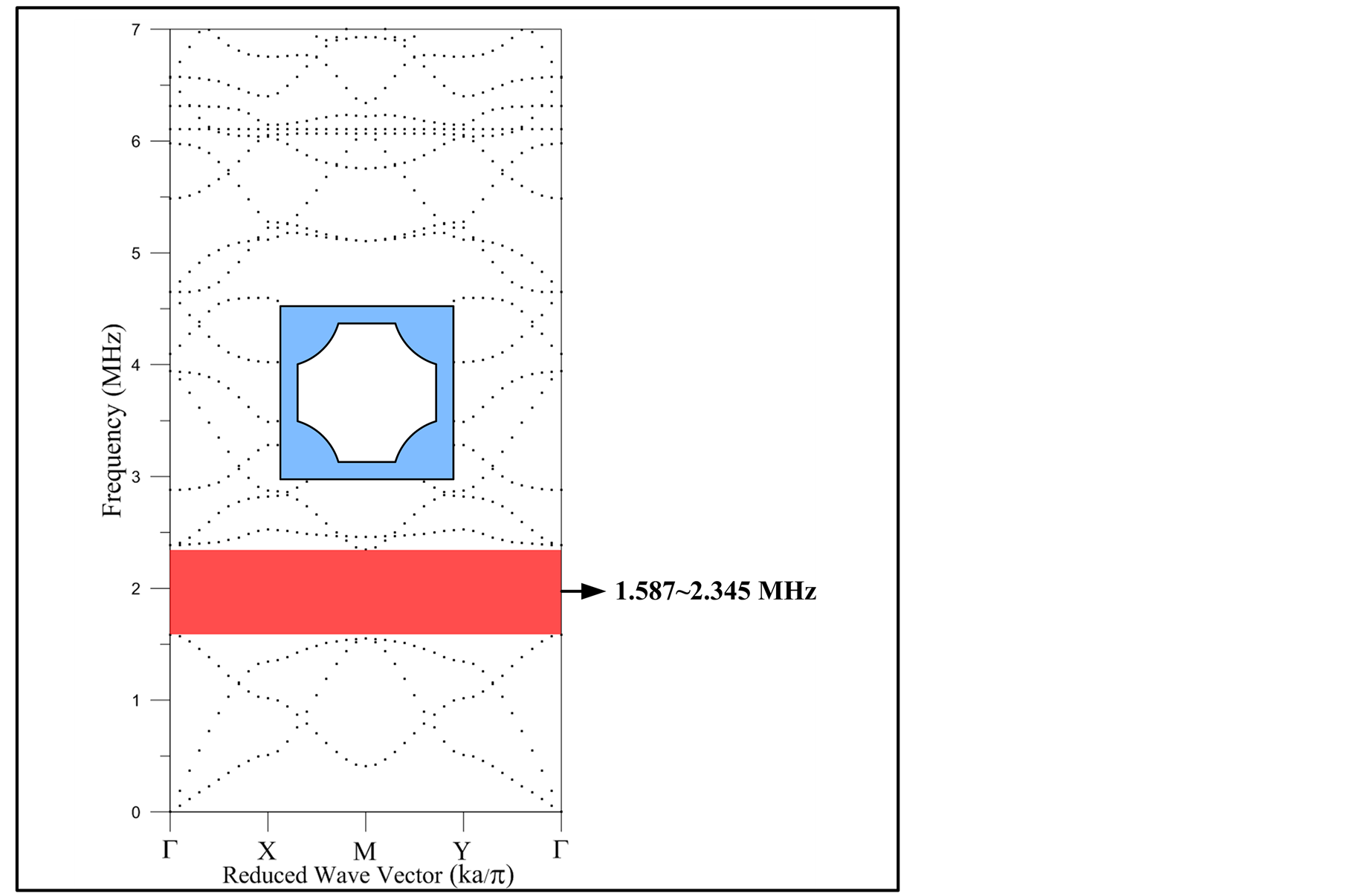
Figure 4. The dispersion curve of the square graphene-like structure (0 - 7 MHz).
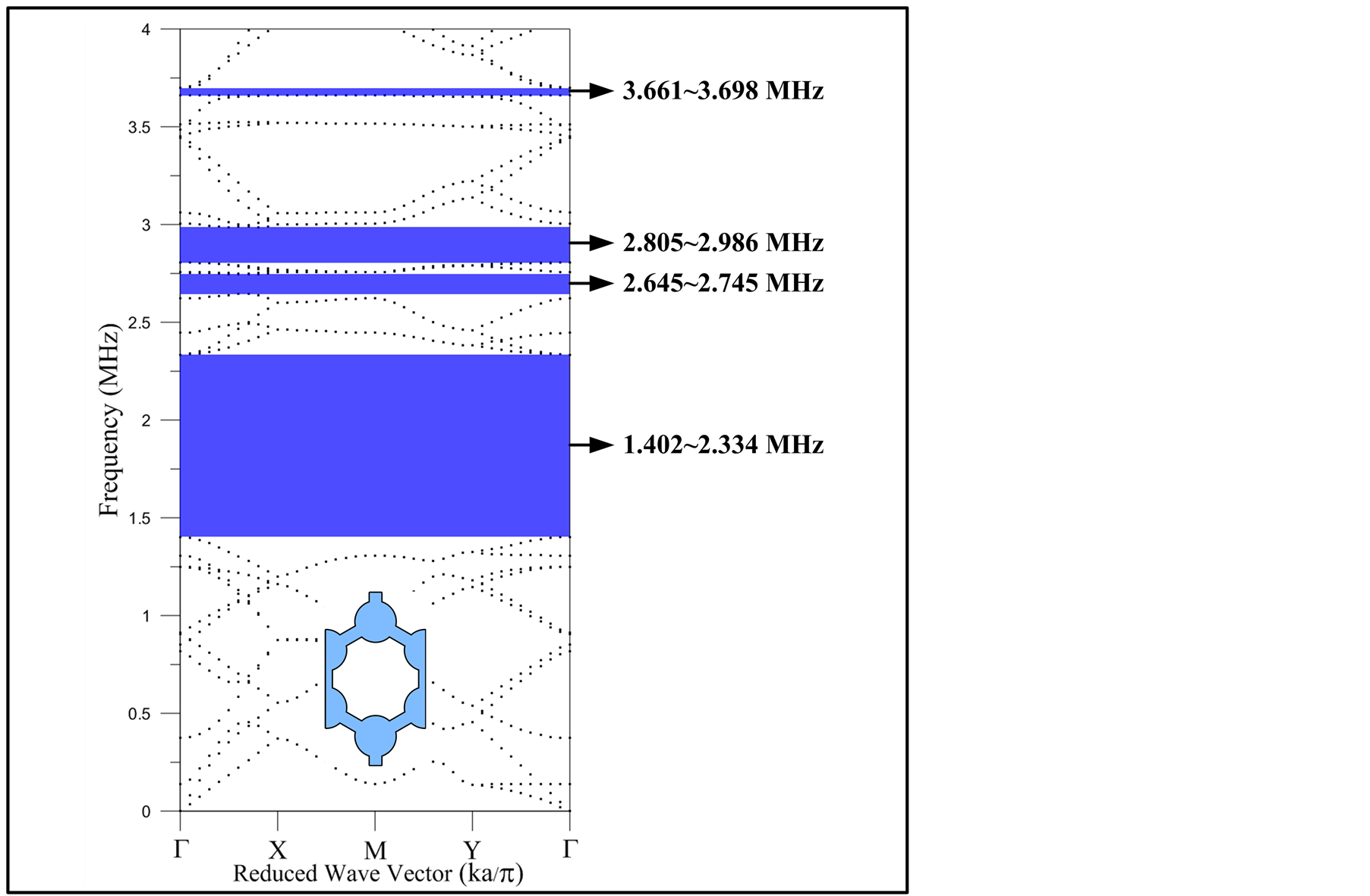
Figure 5. The dispersion curve of the regular hexagonal graphene-like structure (0 - 4 MHz).
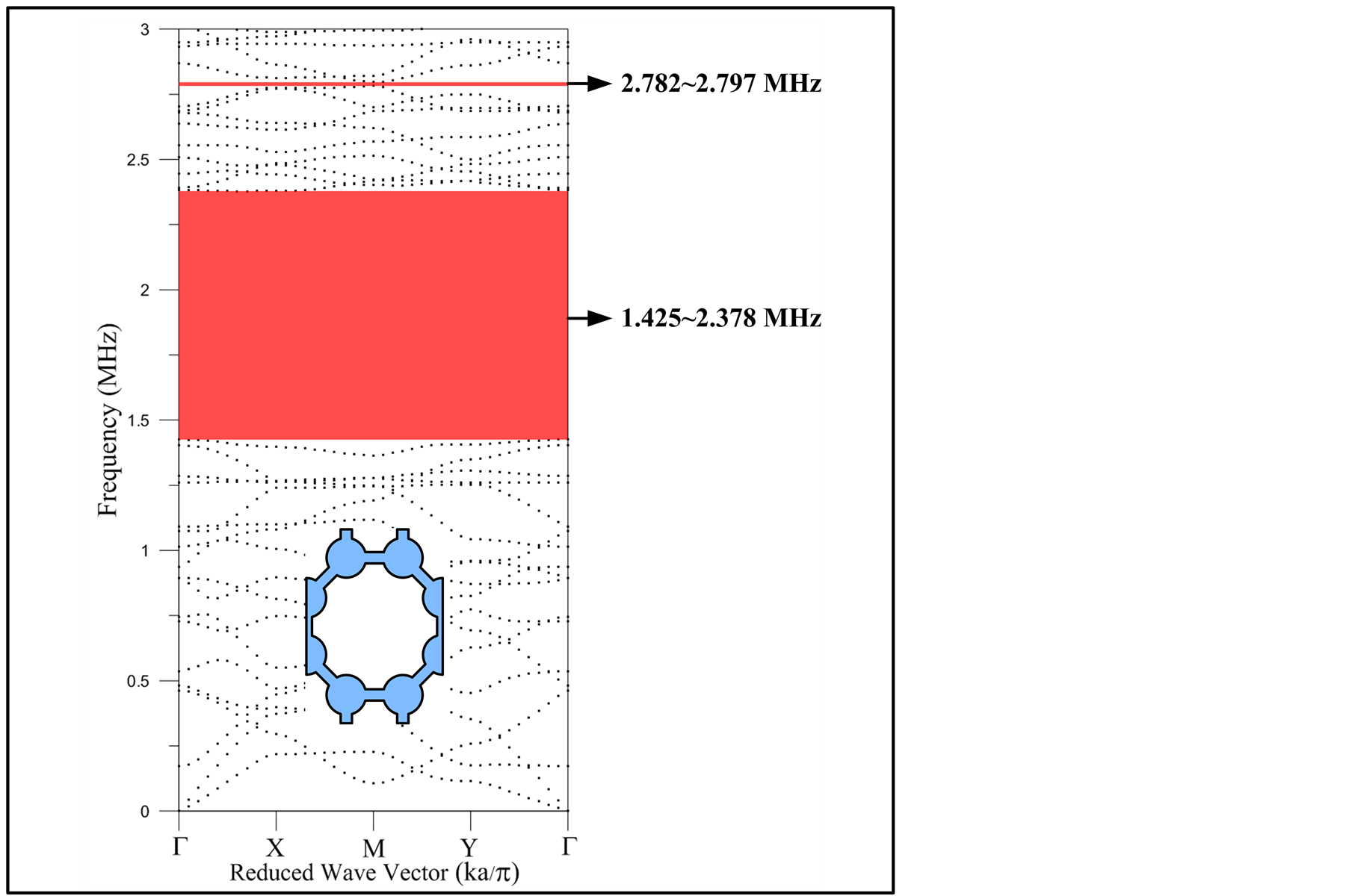
Figure 6. The dispersion curve of the regular octagonal graphene-like structure (0 - 3 MHz).
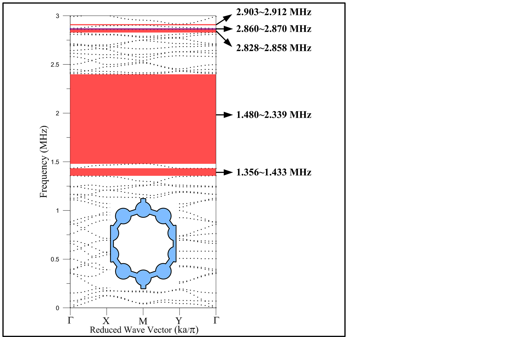
Figure 7. The dispersion curve of the regular decagonal graphene-like structure (0 - 3 MHz).
propagation of certain frequency bands, the 2D graphene-like structure could be designed to accommodate user needs when the number of sides in regular polygons changes.
In phononic crystals, the band gap is categorized into a complete band gap, which inhibits the propagation of acoustic waves in all directions, and a directional band gap, which inhibits the propagation of acoustic waves only in a certain direction. The focus of this study is on complete band gaps. Figures 8 and 9 show the band gap distribution trends of various regular polygonal graphene-like structures; the horizontal axis represents the four regular polygonal structures, the vertical axis represents the size of the band gap, and the unit of measure is MHz. Figure 8 shows that the largest band gap in the four models is located between 1.4 and 2.5 MHz. Among the four polygons, the regular hexagon and octagon possess the optimal band gaps ranging from 1.402 to 2.334 MHz and from 1.425 to 2.378 MHz, respectively, and the band gap sizes are 0.93 MHz and 0.95 MHz, respectively. All four model structures contain numerous complete band gaps. The following phenomena were observed by dividing the observation range into A (1 to 5 MHz) and B (5 to 7 MHz) frequency ranges for further examination.
The bang gap distribution in Range A indicates that the complete band gap effect is known to gradually increase from a low to high frequency when the number of polygon sides changes from 4 (a square) to 10 (a regular decagon; Figure 8). By comparison, a square does not generate a complete band gap in Range B, whereas the other three models generate complete band gaps in the frequency range. Among the regular polygons, a regular octagon has up to 14 complete band gaps in the frequency range of B. However, for Range B, the widest band gaps appear in the regular hexagon model, with the frequency ranging between 5.583 and 5.976 MHz and the band gap size measuring 0.39 MHz (Figure 9). By compiling data from frequency ranges A and B, the study found that both regular octagon and decagon models contained more than 10 complete band gaps. Therefore, significant band gap effects are generated when the compositional conditions of the graphene-like structure (i.e., the number of sides of a polygon) change; these effects can be applied to manufacture new AWDs.
3.2. Resonance Mode Deformation
Phononic crystal vibration is typically propagated in the form of elastic waves. The vibration forms are genera-
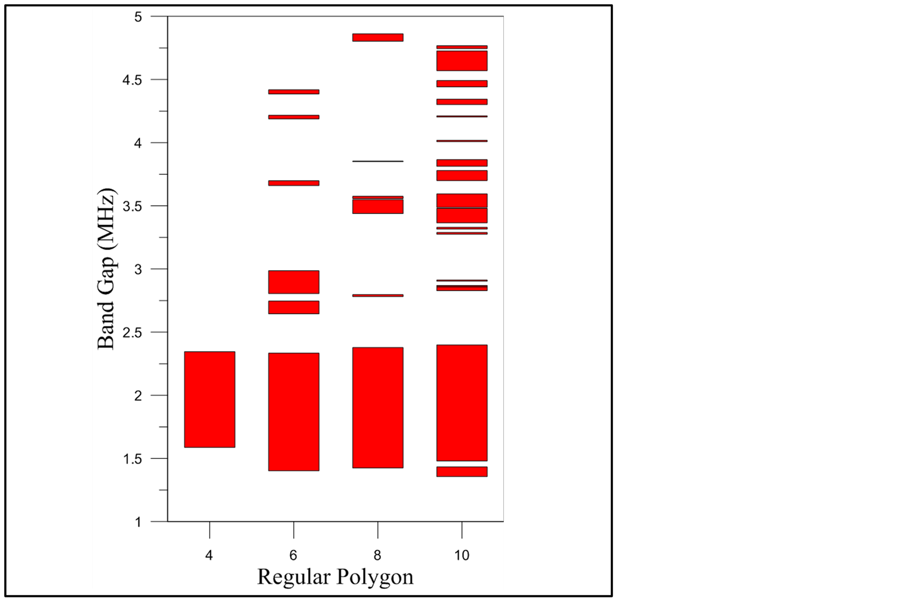
Figure 8. The band gap distribution trends of each regular polygonal graphene-like structure (1 - 5 MHz).
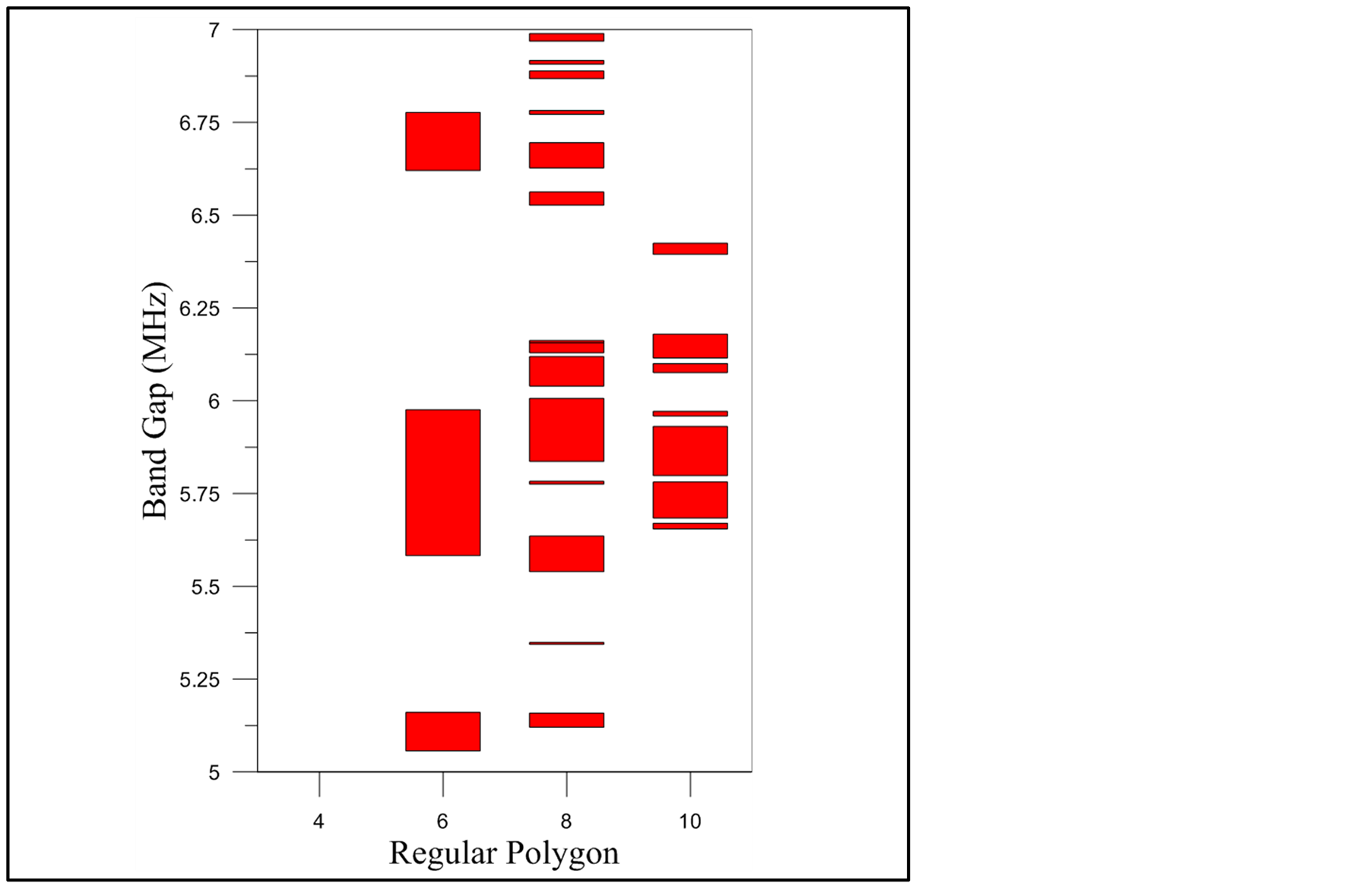
Figure 9. The band gap distribution trends of each regular polygonal graphene-like structure (5 - 7 MHz).
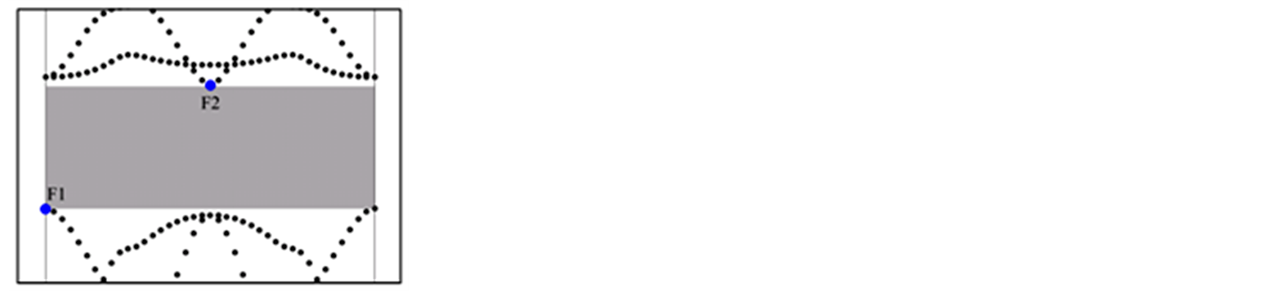
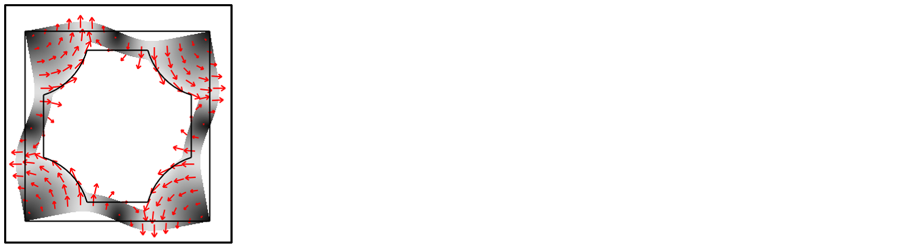
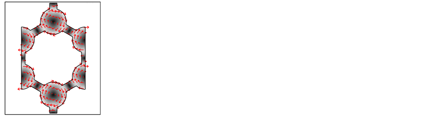
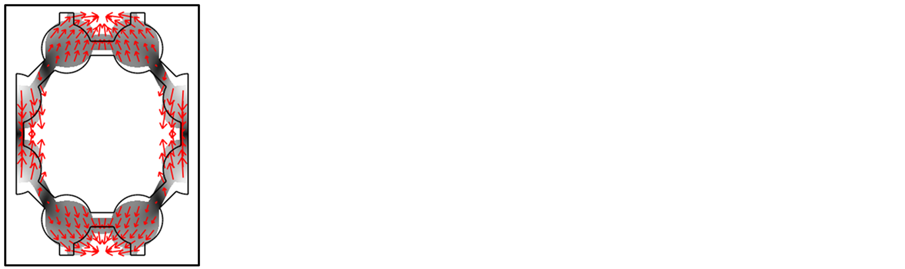
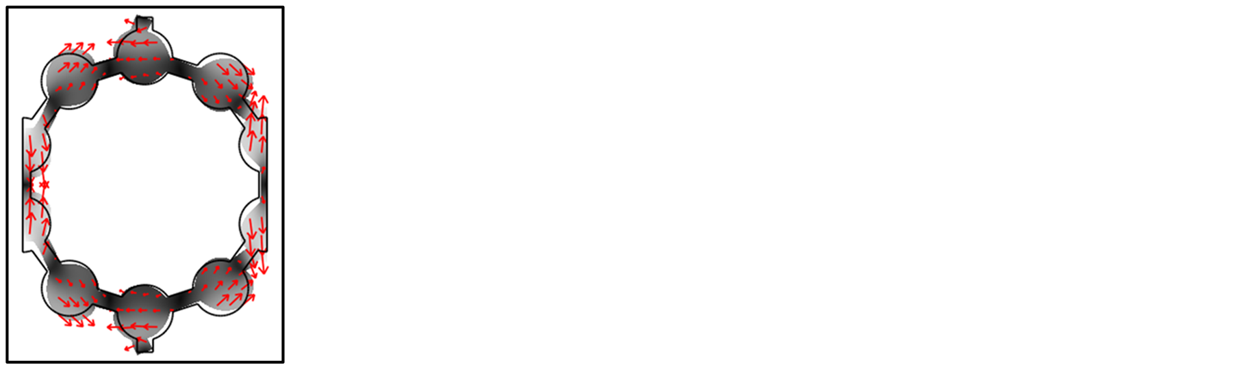
lized as longitudinal and transverse waves and other coupled modes, and elastic waves extend infinitely in the lattice period. Phononic crystals are derived in a manner similar to photonic crystals; thus, phononic crystals have an effect on electrons similar to that of the periodic potential in atoms. Figure 10 shows the energy band structure of a 2D polygonal graphene-like structure in the X-Y mode; the large solid circles in the figure represent the modal frequency of the widest band gaps of the four polygons; the gray areas represent the widest band gaps in the frequency range between 1.4 and 2.5 MHz; and S1 and S2 are the lower and upper boundary of the band gap, respectively. In Figures 11 to 14, (a) and (b) each correspond to the modal frequency at the band gap site of each polygonal structure and the corresponding resonance mode in Figure 10. The direction and length of each arrow represents the displacement and magnitude under natural vibration of the corresponding structure; the gray area represents the 2D graphene-like structure, and the internal material is ZnO.
The vibration mode at the band gap site shows that the bonding circles in the resonance mode of the four polygonal models are twisted and accompanied by compression/tensile deformation. Because of the compression/tensile deformation, the vibrating factors exert a resultant force on the graphene-like structure along the X or Y direction, coupling the longitudinal and transverse waves in the X-Y mode and generating band gaps. For example, regarding the regular octagon and square, the majority of the deformation in the bond diameter of the square appears in a twisted form; only a slight compression/tensile deformation forms at the bonding stick, resulting in a smaller band gap (0.785 MHz). By comparison, most vibration deformations generated in the regular octagon are compression/tensile deformations and cause wider band gaps (0.95 MHz). The coupling effect of the compression/tensile resultant force on primitive unit cells under long wave conditions affects the band gap width; greater resultant forces generate wider band gaps and weaker resultant forces generate narrower band gaps.
4. Conclusion
This study focused on the use of graphene-like structures for developing new AWDs. Graphene-like structures formed from ZnO with strong piezoelectricity were studied to observe the band gap characteristics under natural vibration. Under the conditions of a fixed bond diameter (d = 2R = 0.7 mm), bonding stick width (0.2 mm), and side length (1 mm), this study investigated the effect that changing the number of sides in a 2D graphene-like
 (a)
(a)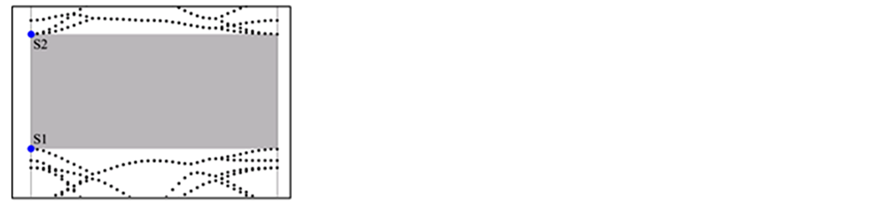 (b)
(b)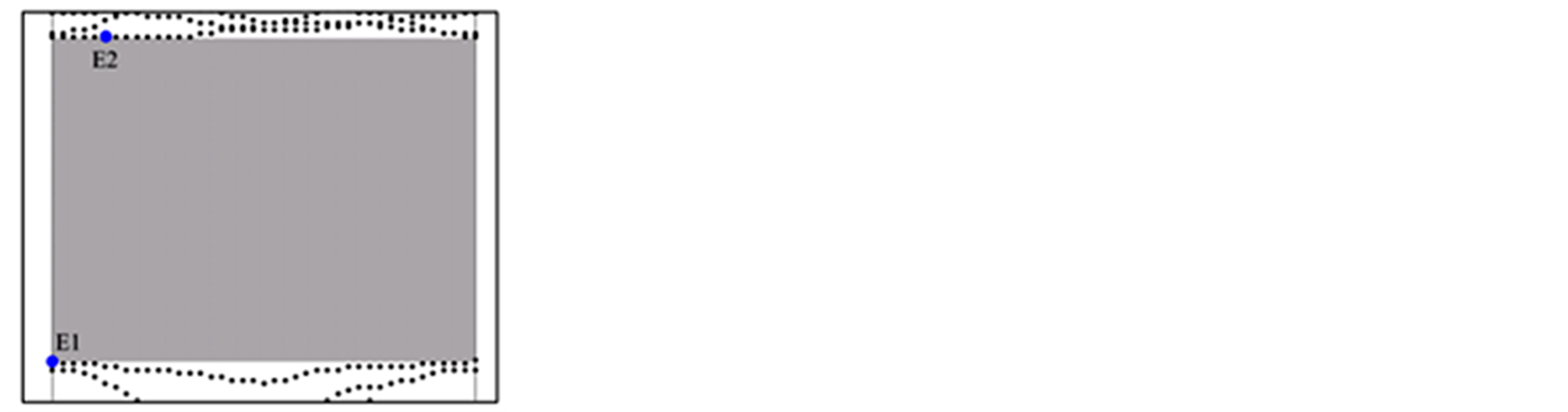 (c)
(c)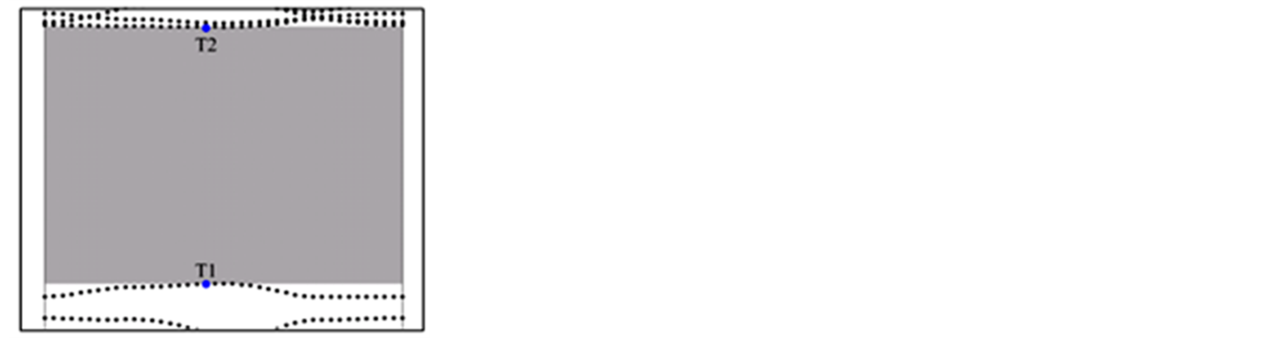 (d)
(d)
Figure 10. The dispersion relationship of the widest band gap in each regular polygonal graphene-like structure (1.4 - 2.5 MHz). (a) square, (b) regular hexagon, (c) regular octagon, (d) regular decagon.
 (a)
(a)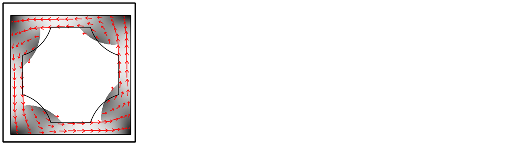 (b)
(b)
Figure 11. The modal vibration pattern at the square graphene-like structure edges (corresponding to Figure 10(a)). (a) Lower boundary of band gap (F1), (b) Upper boundary of band gap (F2).
 (a)
(a)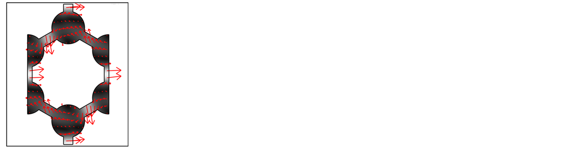 (b)
(b)
Figure 12. The modal vibration pattern at the regular hexagonal graphene-like structure edges (corresponding to Figure 10(b)). (a) Lower boundary of band gap (S1), (b) Upper boundary of band gap (S2).
 (a)
(a)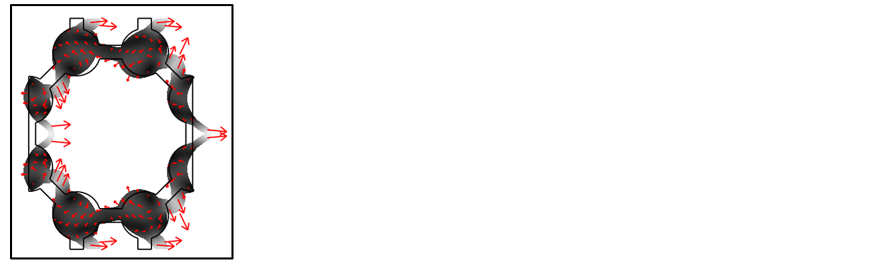 (b)
(b)
Figure 13. The modal vibration pattern at the regular octagonal graphene-like structure edges (corresponding to Figure 10(c)). (a) Lower boundary of band gap (E1), (b) Upper boundary of band gap (E2).
 (a)
(a)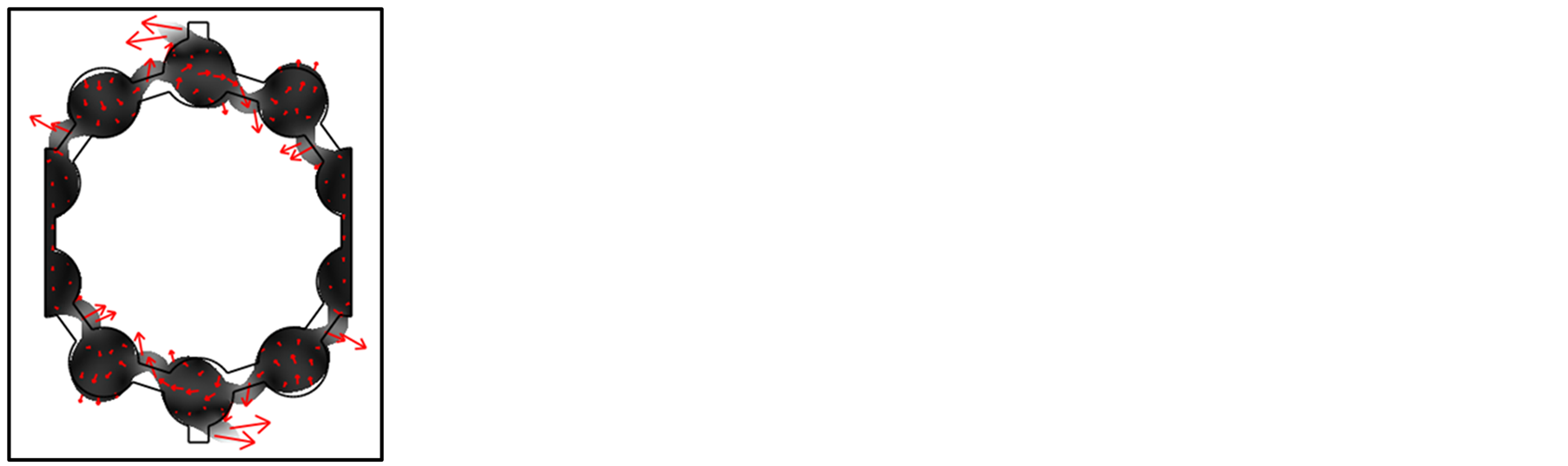 (b)
(b)
Figure 14. The modal vibration pattern at the regular decagonal graphene-like structure edges (corresponding to Figure 10(d)). (a) Lower boundary of band gap (T1), (b) Upper boundary of band gap (T2).
structure has on the vibration band gap characteristics and the vibration mode at the site of the band gap. The polygons used in this study were a square, and a regular hexagon, octagon, and decagon. The analysis showed that all four regular polygonal structures have wider band gaps when the frequency is between 1.4 and 2.5 MHz. Except for the square, all polygons exhibited a filter effect greater than 0.9 MHz; specifically, the regular octagon showed the best filter effect. For vibration analysis in the X-Y mode, modal changes were observed at complete band gap sites. The two major deformations resulted from torsional force and tensile/compression resultant force. The main vibration mode that generates band gaps is the coupling of the resultant force from longitudinal waves in the X direction and transverse waves in the Y direction, which results in compression/tensile deformation. The magnitude of the resultant force is proportional to the band gap width; a greater resultant force generates a larger band gap. Conversely, a weaker resultant force generates a smaller band gap.
Acknowledgements
We thank the National Science Council (Project No. NSC101-2628-E-150-001-MY3) for funding.
References
- Novoselov, K.S., Geim, A.K., Morozov, S.V., Jiang, D., Zhang, Y., Dubonos, S.V., Grigorieva, I.V. and Firsov, A.A. (2004) Electric Field Effect in Atomically Thin Carbon Films. Science, 306, 666-669. http://dx.doi.org/10.1126/science.1102896
- Novoselov, K.S., Geim, A.K., Morozov, S.V., Katsnelson, M.I., Grigorieva, I.V., Dubonos, S.V. and Firsov, A.A. (2005) Two Dimensional Gas of Massless Dirac Fermions in Graphene. Nature, 438, 197-200. http://dx.doi.org/10.1038/nature04233
- Kohlschütter, V. and Haenni, P. (1918) Zur Kenntnis des Graphitischen Kohlenstoffs und der Graphitsäure. Zeitschrift für Anorganische und Allgemeine Chemie, 105, 121-144. http://dx.doi.org/10.1002/zaac.19191050109
- Nair, R.R., Blake, P., Grigorenko, A.N., Novoselov, K.S., Booth, T.J., Stauber, T., Peres, N.M.R. and Geim, A.K. (2008) Fine Structure Constant Defines Visual Transparency of Graphene. Science, 320, 1308. http://dx.doi.org/10.1126/science.1156965
- Ruess, G. and Vogt, F. (1948) Höchstlamellarer Kohlenstoff aus Graphitoxyhydroxyd. Monatshefte für Chemie und verwandte Teile anderer Wissenschaften, 78, 222-242. http://dx.doi.org/10.1007/BF01141527
- Geim, A.K. and Novoselov, K.S. (2007) The Rise of Grapheme. Nature Materials, 6, 183-191. http://dx.doi.org/10.1038/nmat1849
- Bae, S., Kim, H., Lee, Y., Xu, X., Park, J.-S., Zheng, Y., Balakrishnan, J., Lei, T., Kim, H.R., Song, Y.I., Kim, Y.-J., Kim, K.S., Özyilmaz, B., Ahn, J.-H., Hong, B.H. and Iijima, S. (2010)Roll-to-Roll Production of 30-Inch Graphene Films for Transparent Electrodes. Nature Nanotechnology, 5, 574-578. http://dx.doi.org/10.1038/nnano.2010.132
- Berger, C., Song, Z., Li, T., Li, X., Ogbazghi, A.Y., Feng, R., Dai, Z., Marchenkov, A.N., Conrad, E.H., First, P.H. and De Heer, W.A. (2004) Ultrathin Epitaxial Graphite: 2D Electron Gas Properties and a Route toward Graphene-Based Nanoelectronics. The Journal of Physical Chemistry B, 108, 19912-19916. http://dx.doi.org/10.1021/jp040650f
- Han, M.Y., Özyilmaz, B., Zhang, Y. and Kim, P. (2007) Energy Band-Gap Engineering of Graphene Nanoribbons. Physical Review Letters, 98, Article ID: 206805. http://dx.doi.org/10.1103/PhysRevLett.98.206805
- Narendar, S., Mahapatra, R.D. and Gopalakrishnan, S. (2011) Ultrasonic Wave Characteristics of a Monolayer Graphene on Silicon Substrate. Composite Structures, 93, 1997-2009. http://dx.doi.org/10.1016/j.compstruct.2011.02.023
- Kryuchkov, S.V. and Kukhar, E.I. (2013) Charge Dragged by the Solitary Electromagnetic Wave in the Graphene superlattice. Physica E: Low-Dimensional System & Nanostructures, 48, 96-100. http://www.sciencedirect.com/science/article/pii/S1386947712004729
- Zhang, Y., Tang, T.-T., Girit, C., Hao, Z., Martin, M.C., Zettl, A., Crommie, M.F., Shen, Y.R. and Wang, F. (2009) Direct Observation of a Widely Tunable Bandgap in Bilayer Grapheme. Nature, 459, 820. http://dx.doi.org/10.1038/nature08105
- Chandratre, S. and Sharma, P. (2012) Coaxing Graphene to Be Piezoelectric. Applied Physics Letters, 100, Article ID: 023114. http://dx.doi.org/10.1063/1.3676084
- Liu, Z.-F., Liu, N.-H. and Wu, Q.-P. (2012) Magnetoresistance and Shot Noise in Graphene-Based Nanostructure with Effective Exchange Field. Journal of Applied Physics, 112, Article ID: 123719. http://dx.doi.org/10.1063/1.4770494
- Xu, P., Schoelz, J.K., Barber, S.D., Ackerman, M.L. and Thibado, P.M. (2012) Broad Frequency and Amplitude Control of Vibration in Freestanding Graphene via Scanning Tunneling Microscopy with Calculated Dynamic PseudoMagnetic Fields. Journal of Applied Physics, 112, Article ID: 124317. http://dx.doi.org/10.1063/1.4771874
- Killi, M., Wu, S. and Paramekanti, A. (2011) Band Structures of Bilayer Graphene Superlattices. Physical Review Letters, 107, Article ID: 086801. http://dx.doi.org/10.1103/PhysRevLett.107.086801
- Yablonovitch, E. (1987) Inhibited Spontaneous Emission in Solid-State Physicsand Electronics. Physical Review Letters, 58, 2059-2062. http://dx.doi.org/10.1103/PhysRevLett.58.2059
- John, S. (1987) Strong Localization of Photons in Certain Disordered Dielectric Superlattices. Physical Review Letters, 58, 2486-2489. http://dx.doi.org/10.1103/PhysRevLett.58.2486
- Ho, K.M., Chan, C.T. and Soukoulis, C.M. (1990) Existence of a Photonic Gap in Periodic Dielectric Structures. Physical Review Letters, 65, 3152-3155. http://dx.doi.org/10.1103/PhysRevLett.65.3152
- Johnson, S.G. and Joannopoulos, J.D. (2003) PHOTONIC CRYSTALS: The Road from Theory to Practice. Kluwer Academic Publishers, Boston.
- Sigalas, M. and Ecconomou, E.N. (1992) Elastic and Acoustic Wave Band Structure. Journal of Sound and Vibration, 158, 377-382. http://dx.doi.org/10.1016/0022-460X(92)90059-7
- Kushwaha, M.S., Halevi, P., Dobrzynski, L. and Diafari-Rouhani, B. (1993) Acoustic Band Structure of Periodic Elastic Composites. Physical Review Letters, 71, 2022-2025. http://dx.doi.org/10.1103/PhysRevLett.71.2022
- Huang, Z.G. and Chen, Z.Y. (2011) Acoustic Waves in Two-dimensional Phononic Crystals with Reticular Geometric Structures. Journal of Sound and Vibration, 133, Article ID: 031011. http://dx.doi.org/10.1115/1.4003201
- Farzbod, F. and Leamy, M.J. (2011) Analysis of Bloch’s Method in Structures with Energy Dissipation. Journal of Sound and Vibration, 133, Article ID: 051010. http://dx.doi.org/10.1115/1.4003943
- Huang, Z.G. (2011) Silicon-Based Filters, Resonators and Acoustic Channels with Phononic Crystal Structures. Journal of Physics D: Applied Physics, 44, Article ID: 245406. http://dx.doi.org/10.1088/0022-3727/44/24/245406
- Wu, T.-T., Huang, Z.G., Tsai, T.C. and Wu, T.C. (2008) Evidence of Complete Band Gap and Resonances in a Plate with Periodic Stubbed Surface. Applied Physics Letters, 93, Article ID: 111902. http://dx.doi.org/10.1063/1.2970992
- Sigalas, M.M. and Koukaras, E.N. (2012) Phononic Band Gaps in Graphene-Based Materials. Applied Physics Letters, 100, Article ID: 203109. http://dx.doi.org/10.1063/1.4717746
NOTES

*Corresponding author.