Open Journal of Applied Sciences
Vol.09 No.06(2019), Article ID:92938,29 pages
10.4236/ojapps.2019.96037
The Spin Torus Energy Model and Electricity
David Johnson
Retired IT Lecturer, Perth, Australia

Copyright © 2019 by author(s) and Scientific Research Publishing Inc.
This work is licensed under the Creative Commons Attribution International License (CC BY 4.0).
http://creativecommons.org/licenses/by/4.0/


Received: January 23, 2019; Accepted: June 7, 2019; Published: June 10, 2019
ABSTRACT
Defining the electron to be a toroidal form of concentrated energy rather than a monopole point-charge, such as used for the Orbital Nuclear Atomic Model (ONAM), leads to a subtly different explanation for electricity and the dynamic nature of electromagnetic fields. The Spin Torus Energy Model (STEM) is used to define the electron and positron, which are then used to explain the nature of electric and magnetic fields, electric current generation from battery and induction sources, capacitor charge and discharge, and superconductivity. STEM supports the notion that free positrons exist within matter, and are equal in importance to electrons: as ONAM makes no provision for positrons within matter, this assertion has wide ranging implications for atomic structure models and chemistry.
Keywords:
Electron, Positron, Bitron, Electromagnetic, Energy, Chiral, Torus, Induction, Electricity, Electric Field, Magnetic Field, Electrostatic Charge, Static, Attraction, Repulsion, Capacitor, Hole, Superconductivity

1. Introduction
The Orbital Nuclear Atomic Model (ONAM) defines the electron as a point-form monopole electric charge for mathematical modelling purposes, with the electron commonly represented as a spinning sphere simply labelled “e−”.
A well-documented alternative model to monopole point-charge is the Toroidal Solenoidal Electron (TSE) [1] [2] [3] which defines the electron as a spinning point electric charge that moves at high speeds in a solenoidal pattern around a torus-shaped pathway: examples of variations of the TSE model [1] [4] - [9] are shown in Figure 1. The mathematics developed for the TSE [7] [8] [9] [10] model is claimed to provide a better fit for the electromagnetic characteristics of electrons than the monopole point-charge model.
The Spin Torus Energy Model (STEM) consists of concentrated core energy

Figure 1. Examples of electron/positron torus-based models.
flowing or spinning at close to the speed of light as a fluid-like continuum in the circular pathway of a torus. STEM is a hybrid model that is distinctly different to both the monopole point-charge and the TSE models, but shares aspects of both. A basic STEM particle is the bitron, which can be induced to transform into either an electron or a positron by an appropriate electromagnetic field.
The spin of a bitron’s concentrated core energy generates an apparent centrifugal force1 around its outer equatorial perimeter, and because the ductile strength of the core has been exceeded, a stream of energy weeps from the equatorial perimeter. The escaped energy is much less concentrated than core energy and forms a relatively stable disk-like shim around and spinning in synch with the core energy of the bitron. A bitron with a stable disc-like outer energy field as shown in Figure 2(a) is referred to as a neutral bitron.
The energy field of a neutral bitron is not dissimilar to accretion disks (Figure 2(b)) observed around massive centralised astrological objects. Accretion disks are considered to be caused by MRI (Magneto-Rotational Instability, as variously called Balbus-Hawley or Velikhov-Chandrasekhar instability). Although one phenomenon is sub-microscopic and the other is macroscopic, the cause of both would appear to be MRI related.
Neutral bitrons do not have chirality2 and, although they have the same contained energy levels of electrons and positrons, they are neither an electron nor a positron. However, an externally applied electromagnetic field can change the dynamics of a neutral bitron’s energy field instantaneously, providing it with chirality and transforming it into either an electron or a positron. The bitron is then considered to be polarised.

Figure 2. Neutral bitron.
An applied electromagnetic field pushes an amenable neutral bitron’s outer energy field towards one of its two axial extremities where it folds back towards the central hole of the energy core torus. As the energy field approaches the central hole of the energy core, its circular spin radius is reduced causing it to accelerate and to form a convergent inward-flow vortex [11] . Although some of the energy field’s energy may be absorbed by the core energy, most of the returning energy passes through the torus’s central hole to spiral outwards on the other side as a swirling energy field, expanding to form a divergent outward-flow vortex. The field energy then folds back to join the energy field streaming from the torus circumference, forming a re-circulating atmosphere of low concentration energy circulating around the energy core as shown in Figure 3(b).
The pattern of a polarised bitron’s the energy field is superficially similar to that of a magnetic field, with the convergent vortex resembling a magnetic South pole and the divergent vortex a magnetic North pole: however it is different to a magnetic field because it has a circular flow component that a magnetic field does not have.
Chirality is a subtle property that warrants further discussion. When looking at a bitron from one side, should its core energy appear to flow in a clockwise direction, then by rotating it by 180˚ perpendicular to its spin axis, or by simply looking at it from the other direction, it will appear to flow in an anti-clockwise direction (see Figure 3(a)). That is not chirality. However when circular flow is combined with a linear flow direction we have chirality: a perfect chiral analogy is the incompatibility between a left-thread and a right-thread screw.
As a polarised bitron’s energy field has both a linear (i.e. axial) and a circular flow component, it is chiral and the chiral form of the energy field that determines whether it has become an electron or a positron.
A convention is required to identify the chiral form of a polarised bitron’s energy field. In order to minimise confusion with common-use electromagnetic field terminology such as North/South, Positive/Negative and left/right nomenclature has been avoided. Instead a clockwise/anti-clockwise and in/out-flow terminology has been adopted, abbreviated by use of a dual-letter notation.

Figure 3. Electron and positron field patterns.
The first letter of the notation identifies circular spin direction of the energy core/field: a “C” for Clockwise when looking along the spin axis towards the bitron, and an “A” for Anti-clockwise. The 2nd letter is for the central axial in/out-flow direction of the energy field: an “I” to represent In-flow of the convergent vortex, and an “O” for Out-flow of the divergent vortex away from the torus hole.
Note that the linear flow direction close to the spin axis within the flow vortices is in the opposite direction to flow direction around the outside of the energy core: thus the “I” and “O” notations refer only to the flow direction close to the spin axis within the divergent and convergent vortex areas. Also, when used, the circular flow component is notated as “e” (left in Figure 3(a)) and linear component “b” refer to the outer zone (external) energy field flow components.
Using this simple dual-letter notation, the convention adopted is that an electron is defined and identifiable by an AO and CI combination, and a positron by a CO and AI combination. Due to chirality, only one end of the energy field needs to be established using the dual-letter notation to distinguish between an electron and a positron.
An important aspect of the STEM electron is that it can be easily converted into a positron by simply reversing or flipping the axial flow direction of its energy field. Energy field flipping also works in reverse, converting a positon into an electron, and does so without having to change the orientation of the torus energy core. Field flipping allows STEM to readily explain AC electricity and Beta decay, which for the latter involves the transformation of protons to neutrons and vice versa [12] .
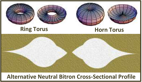
Figure 3(b) shows a more stylised depiction of a positron energy field flows: it also shows the position of the equatorial field energy disk when the bitron assumes neutral mode, with the hollow arrows indicating the direction in which the neutral energy disk was pushed to create the positron energy field pattern. It also shows the ring torus as being thin with a wide central hole, whereas Figure 1(a) and Figure 2(a) show a thicker ring torus with a smaller hole. It could also be closer to a horn torus as shown below. Mathematical modelling should shed more light as to the bitron’s core energy geometry: it might even have a flying-saucer-like cross-sectional profile as shown below. Any variation to the suggested geometry would need a central hole similar to that of a torus core to facilitate the flow of polarised energy fields.
Now that a definition and notation for an electron and positron have been established in terms of energy core and field flows, the nature of electric currents, electric and magnetic fields and electromagnetic attraction and repulsion can be explored and explained in energy specific terms.
2. Electric Currents
Within an electrical conductor the energy fields of free neutral bitrons cause them to become axially aligned with approximately equal numbers facing one way (clockwise say) and the other half the other (anti-clockwise say). The axially aligned bitrons become grouped into like-spin strands in which the member bitrons are evenly spaced. A good conductor allows the formation of longer, less contorted bitron strands and are characterised by less obstructions in terms of atomic and chemical structure, hairline faults and crystal faces.
An electric current can be generated within a conductor (e.g. a copper wire conductor) by electromagnetic induction or by a source/sink mechanism. We shall now concentrate upon the source/sink generation of an electric current, with electromagnetic induction being addressed in Chapter 4.
The source/sink mechanism involves the creation of electron and positron concentrations which represent supply sources and cause migration of electrons and positrons to lower concentration sinks. Electron and positron concentrations can be created by a variety of processes: chemical reactions (e.g. batteries), thermo-electric processes, the photoelectric effect, static electricity, surface effects (plasmons [13] ) and capacitor charge and discharge. In this paper we shall just be considering the effect of such concentrations rather than their cause.
A simple electric circuit can be considered to consist of an electron source (the negative terminal) connected to a positron source (the positive terminal) by an electrical conductor (e.g. copper wire). Within such a circuit electrons and positrons move with their out-flow poles (AO and CO respectively) facing the direction of travel: the reason for this will soon become apparent.
As electrons enter the electron supply end of a conductor (the large red minus sign in Figure 4), they form or join electron-strands (or e-strands) with their AO poles directed towards the positive terminal end. The newly energized e-strands at the negative terminal end induce the energy fields of adjacent neutral bitron strands that have the same circular spin direction as themselves to polarise. This process turns into a chain reaction as induced e-strands induce their neighbouring compatible neutral strands to polarise. As the supply of more electrons continues the e-strands continue to build and to increase in number, strength and packing density.
Simultaneously, on the positive terminal supply side of the circuit, positrons are added with their CO end facing the negative terminal, so creating and strengthening positron-strands (or p-strands). The net result is that the circuit becomes energised by e- and p-strands that all have the same spin direction (as can be clearly seen in Figure 4) and orientated with their energy field out-flows pointing in opposite directions. Within their respective strands electrons and positrons can be considered to represent small electric dipoles with implicit positive (CO and CI) and implicit negative (AO and CI) poles, as shown the strand representation at the top of Figure 4, which helps keep them together within their strands as they move.
Only half the available neutral strands in the conductor are polarised: the other half, those with opposite spin, remain as neutral strands interspersed amongst the polarised strands. Of the polarised strands, half are e-strands and half are p-strands. The solenoid-like flow of the outer energy field of polarised strands pushes screw-like against the neutral strands, thrusting the polarised strands forwards. The opposite chirality of the e- and p-strands causes them to move in

Figure 4. Electric current: electron and positron movement.
opposite directions leading with their AO and CO respective poles foremost. The neutral strands, on the other hand, are pushed back and forward in opposite directions by the polarised strands resulting in no overall change of position: they just fibrillate and dance on the one spot.
Although partially offset by the neutral strand spin, polarised strands are more energised and the net circular component (e) of their polarised energy fields generates an induced magnetic field around the current-carrying wire conductor. However, with the axial linear component of the energy fields (b) of the e- and p-strands is in opposite directions, they cancel each other out.
When the positive and negative terminal ends are reversed, the strands with opposite spin that were not polarised now become polarised, and both the current and induced magnetic field around the wire conductor reverse direction. Thus AC electricity cycles reflect the alternating polarisation of strands with opposite circular spin direction.
The strong energy fields associated with e- and p-strands present as positive and negative electric fields whenever they extend beyond the end of a wire conductor, such as when two probes are attached to the positive and negative side of a battery. As stated earlier, electric fields have a circular spin component to their flow pattern, whereas magnetic fields consist of linear flow without any circular component. Both types of energy fields consist of the same type of energy but they just have different flow patterns.
In the way of a summary, STEM contends that, rather than being the one-way movement of electrons, electricity is the two-way movement of polarised e- and p-strands which, with the help of the neutral strands of opposite spin direction, push themselves in opposite directions to each other, leading with their AO and CO poles respectively. It is a simple, logical model that fits all the known facts related to electricity without the need to invoke fictitious positive hole and electric dipole constructs.
A subtle difference between the STEM and the TSE models is that STEM core energy flow is purely circular spin and is thus non-chiral, whereas the solenoidal nature of the TSE core energy makes the core itself chiral as reflected in the chirality of the associated energy field: it has no neutral mode. A result of this subtle, but important difference, is that the TSE model requires that all electrons and positrons to be flipped (i.e. be rotated by 180˚) in order to change current direction, which is considered to be untenable.
3. Electric Circuits and Electric Fields
For this discussion an electric circuit is considered to comprise of a power source and various electrical components connected by a copper wire conductor that supports the two way movement of polarised e- and p-strands. In order to more fully explore and explain the behaviour of bitron strands in relationship to an electric circuit, the following three states of a basic electric DC circuit will be considered:
1) No power source;
2) Open circuit with power source connected; and
3) Power source in place but with a break of circuit (switched off mode).
1) No power source
This option relates to a length of copper wire that is not connected to any circuitry. The neutral bitron strands are variously bent in by the electromagnetic fields within the wire’s atomic lattice, but remain largely intact. Apart from possible heat-related jostling and buffeting, there is no directional movement of the strands or significant polarisation of the bitrons’ energy fields: they are all essentially in neutral mode. With approximately equal numbers of clockwise and anti-clockwise oriented strands, the circular spin components of their energy fields cancel each other out so that no induced circular magnetic field results.
2) Open circuit with power source connected
When an energy source starts polarising that half of the neutral strands with the appropriate circular spin direction, the newly energised polarised strands break free from local electro-magnetic fields within the wire’s atomic lattice, possibly straightening out somewhat in the process, and, by pushing against the neutral strands with opposite spin, start to move in opposite directions as an electric current. The p-strands work their way towards the negative terminal and e-strands towards the positive terminal.
The negative side of an open electric circuit thus acts as an electron source and a positron sink, and the positive side a positron source and an electron sink, resulting in a reciprocating source-to-sink model for electricity flow. Induced electric currents have implied (or virtual) positive and negative sources and sinks, whereas currents generated by chemical energy means (e.g. batteries) have physical sources and sinks.
The circular spin component of the e- and p-strand fields (e in Figure 4) combine to create a circular magnetic field around the outside of the wire in a direction conforming with Maxwell’s Right-Hand Grip for electron strands; Maxwell’s Cork Screw Rule applies to both electron and positron strands (see insets lower right in Figure 4). The along-wire magnetic field components (b) moving outer zone of the electron and positron strands are in opposite directions and so cancel each other out.
The electromagnetic energy flowing through the centre of each core energy torus within a polarised strand combines so as to form a strong uninterrupted tunnel-like flow as indicated by the orange/gold arrows in the upper part of Figure 4. The central strand-related energy flow is most important because it is responsible for the instantaneous nature of energy transfer by electricity as well as the formation of the electric field patterns associated with electric point charges, as will be discussed shortly.
The emf (electromagnetic force or voltage as measured in volts) across an electric circuit is a measure of the extent of polarisation of bitron strands. Electric current, as measured in amperes, is defined as the amount of the electric charge (i.e. electrons and positrons combined) passing a fixed point in the circuit per unit time. The movement of electron and positron strands is quite slow (in the order of 80 centimetres per hour), and it is the energy flow through the centre of polarised strands that is responsible for the instant availability of power across an open electric circuit.
Whenever an obstacle is encountered within an electric circuit (e.g. a resistor), the two-way movement between electron and positron strands is restricted, causing a proportional change in electric current. For a resistance forming the load for an electric circuit, Ohm’s Law indicates that for a resistor of R ohms (Ω) and an electric potential difference of V volts the resulting electric current is V/R amperes when the circuit is open.
3) Power source in place but with a break of circuit (switched off mode)
Should a pair of probes be attached to an energy source (e.g. a battery or A-to-D converter) then we have a power source with a break of circuit (i.e. a section of the circuit that is in OFF mode); when the probes are brought together directly, or indirectly via other circuitry, we have an open circuit. When in OFF mode, the rounded tips of each probe can be used to approximate one half of a pair of spherical monopole electric charges as in Figure 5.

Figure 5. Monopole electric field attraction and repulsion.
In OFF mode, on the negative side of the circuit those negatively polarised bitron strands remain polarised just as they would be should the circuit remained open, and continue to push themselves towards the positive terminal but are unable to move forward due to the circuit break; instead the e-strands compress and concentrate within the probe tip, whereas the p-strands, cut off from their source of polarising energy, simply revert back to neutral strands. With only 1/4 of the available strands e-strand energized, any induced magnetic field around the wire and probes is subsumed by the electric field of the probe.
The energy fields of the stationary e-strands that are concentrated at the outer surface of the probe tip with their AO poles pointing outward extend beyond the probe tip, presenting as a negative electric field. Depending upon the strength of the power supply, their combined energised energy fields can extend well beyond the end of the probe tip. The same process is active on the positive side of the break of circuit to create a positive electric field.
As shown in Figure 5, the energised strand fields display patterns analogous to electric lines of force. With STEM the lines of force (considered by conventional Science to be imaginary continuous lines or curves drawn in an electric field to indicate the direction of the electric force) have a physical explanation and justification, and are not imaginary. The spherical equipotential lines for the electric fields around the electric point charges are also shown as blue and red dashed circles.
As the two probes are brought together, the attraction between their negative (AO) and positive (CO) electric fields increases, with the polarised strands starting to induce polarisation of same-spin neutral strands within the approaching probe: as the probes are about to touch the energy transfer is so great that some electrons and positrons, being pushed from behind and pulled by attraction in front, prematurely jump the gap, ionising other molecules in their way and interacting with each other as they go, so generating heat and light ranging from an electric spark to an electric arc. By the time that the two probes are in physical contact with each other (i.e. the circuit is now open or ON), the polarisation of electron and positron strands throughout the circuit is complete and the current is flowing.
4. Electromagnetic Induction
Faraday’s Law of electro-magnetic induction states that whenever a conductor is forcefully moved in an electromagnetic field, an emf is induced which causes a current to flow. For STEM, the current flow represents the synchronous movement in opposite directions of aligned e- and p-strands within the conductor.
In Figure 6, a rod conductor (PQ) forms closure to a “U” shaped electric circuit subjected to a uniform external magnetic field (B). When the rod moves (at

Figure 6. Magnetic field induced current.
speed v) towards the base of the “U” as in Figure 6(a) (thus creating a smaller loop area) a clockwise electric current (I) is generated, nominally from a positive Q to a negative P. When the rod moves in the other direction, away from the base of the “U” as in Figure 6(b) (thus creating a larger loop area), an anti-clockwise electric current (I) is generated, which by convention is nominally from a positive P to a negative Q.
As stated earlier, within a neutral wire conductor not connected to any power source, its bitron strands are variously bent by the electromagnetic fields within the wire’s atomic lattice, but in spite of various twists and turns, the strands remain largely intact. Thus the orientation of bitrons within neutral strands can vary from being axially aligned to the rod (B and E in Figure 6) to being perpendicular to the rod wall (not shown), with an average orientation 45˚ to each (shown as the bitrons A, C, D and F in Figure 6).
The magnetic field direction downwards into the page is shown is shown as  arrow-quill symbol (representing the disappearing cross-quills of an arrow fired through the page): the small attached red arrow represents the relative movement of the magnetic field due to the rod moving towards it.
A neutral bitron is represented by the icon  where the arrow-quill symbol indicates the bitron’s spin direction (here into the page on the right-hand side to represent clockwise spin as viewed from the bottom of the page).
The diagram below shows vertical cross-sections of the bar PQ. When moved right through the magnetic field it distorts the field, shown as the bent lines of force. The magnetic field applies a force in the opposite direction in response to being pushed aside, as shown by the hollow red arrow in Figure 6. When the rod moves to the left a reaction force similarly pushes right. When the bar is stationary, the lines of force tend to wrap around the rod so that any reaction forces on either side counteract each other.
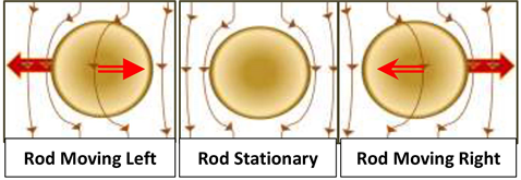
First, considering Figure 6(b) that represents the situation when the rod is moved to the right. For a bitron with orientation D, its leading edge of its energy field has the same direction is in the same direction (downwards) as the approaching magnetic flux field, and thus it gains in spin speed (increased angular momentum). In its more energized state, the reaction force pushes its energy field in the direction of the hollow red arrow to form the AO-CI pattern of an electron. Using similar reasoning, bitrons orientated similarly to bitron F in Figure 6 become CO-AI positrons.
For bitrons axially aligned to the long axis of the rod (here E), their energy fields are aligned to the passing magnetic field’s reaction force and so are unaffected, remaining neutral.
With the rod being moved right, bitrons orientated similarly to A, B and C are partially de-energized because their leading edge flow direction is opposite to that of the magnetic field; they lose spin velocity and thus angular momentum. When their energy fields are pushed out of the neutral position by the magnetic flux, they have insufficient energy to form into electrons or positron, and keep their neutral orientation. As the magnetic flux passes their trailing edge, they regain most of their lost spin speed and angular momentum. Bitrons with orientations such as those of A, B and C are not polarised and thus have no a pro-active role in the formation of electrons and positrons as the rod moves right.
The above description of electron and positron creation relates to isolated bitrons, but within strands within a conductor, bitrons are closely packed and all bitrons within a strand are polarised together, even if the orientation of some strand members have an orientation not favourable to induction form the magnetic field. The stronger the magnetic field or the faster the movement of the rod, the more effective and complete is strand polarisation.
However, it requires energy to keep the e- and p-strands polarised and moving, and the poorer the conductivity of the wire conductor the larger are the energy loss. Unless you have super conductor circuitry, an ongoing energy supply is required to keep the current flowing, As soon as the magnetic field is removed or the movement through the magnetic field is stopped, so is the electric current, and the polarised strands revert back into neutral strands.
Thus, for the bar moving outwards situation, the e-strands start to work their way towards the P end of the rod, leading with their AO end forward, so creating an implicit positive terminal at the P end of the rod. Similarly an implicit negative terminal is created at the Q end of the rod is created by the movement of p-strands leading with their CO end. Although the mechanics of induced current generation is different to the source-sink process, both processes result in one half of the bitron strands (here those corresponding to D, E and F) forming an electric current and the other half remaining neutral (here A, B and C), which in itself is quite remarkable.
When the bar moves to the left (Figure 6(a)), an implicit negative terminal at the P end and a positive terminal at the Q end so that the electric current flows in the opposite direction.
Energy sources such as chemical batteries and A-to-D converters generate electric currents by creating an electron source and positron sink situation that defines a physical negative terminal, and a positron source and electron sink defining a physical positive terminal. Induced electric currents do not require positive and negative terminals but the rod can be considered to be an energy source for the resistor (R) side of the circuit, complete with implicit positive and negative terminal. The difference between the two situations is quite subtle both conceptually and physically.
The physics of generating an electric current by moving a magnet through a closed loop circuit is not dissimilar to generating one by moving a rod conductor through a magnetic field. In order to simplify the description, consider the cross-sectional view of the rod for the moving rod example shown in Figure 7: the blue arrows show the relative movement of the magnetic lines of flux towards the rod and the arrow-quill icon shows the movement of e-strand fields into the page; the arrow-tip icon show their movement out of the page.
Using Maxwell’s Right Hand Rule and assuming that the circular flow direction of electron strands can be defined by the flux line direction in the area adjacent to the blue arrows (i.e. the approaching lines of flux side), the thumb points into the page for the “Rod Moving Right” diagram, and out of the page for the other diagram.
The electromagnetic induction of a loop circuit caused by moving a magnet towards and away from it in different N-S polar orientations is shown in Figure 8.

Figure 7. Induced current patterns.

Figure 8. Magnet-motion induced current within a loop.
Once again, the direction of the approaching lines of flux is shown by the blue arrows, with the circular direction of magnetic flux shown as orange arrowed arcs. The flow direction of the electron strands is shown in cross-sectional views of the loop (AB, CD, EF and GH) as determined by using Figure 7 flows as a template. What could be simpler?
Alternating current (AC) is created by switching the direction of the induced current at a specific frequency. The techniques for creating AC electricity from induced currents are well documented, as are the ways of creating and managing DC electricity: consequently these subjects will not be addressed in this paper.
STEM provides a simple, consistent causative explanation for induced current, its direction and the associated circular magnetic field. Current Science texts and associated articles provide descriptive explanation rather than a causative explanation of these phenomena. They do this by providing a series of inter-related rules and conventions, but no physical explanation, which unfortunately adds a lot of mystery and confusion around electromagnetic induction and electricity.
5. Electrostatic Charges
An electrostatic charge, often called static electricity, is a surface collection of electrically charged particles that is typically generated by the rubbing together of certain materials. The ONAM explanation for static electricity is that triboelectric materials have a tendency to give up electrons so as to become positive (+) in charge, or to attract electrons to become negative (−) in charge. The STEM explanation is that static electricity is due to friction-induced polarisation of neutral and weakly polarised bitron strands, with the structure of triboelectric materials pre-disposing them to develop more p-strands or more e-strands, and “neutral” materials developing approximately equal numbers of each which are less energised and thus become only weakly polarised.
The Triboelectric Series is simply a list of which materials have a tendency to become positively charged, such as air, leather, rabbit fur, glass, human hair, nylon, wool, lead, cat fur, silk, aluminum, paper; and those with a tendency to become negative, such as ebonite, silicone, rubber, teflon, silicon, polypropylene vinyl (PVC), polyethylene (e.g. Scotch and Cello tape), plastic wrap, styrene/styrofoam, polyester, acetate, rayon; and those with a tendency to remain electrostatically neutral, such as cotton and steel. The degree of polarisation varies according to the situation (e.g. contact surface area), the vigor applied and material combination involved.
The STEM explanation for the generation of static electricity is that when two matching positive and negative triboelectric materials are rubbed together, many neutral bitrons with the same spin direction are energetically forced past each other in the opposite direction, their energy fields of their bitron strands interact, mechanically pushing each other in the direction of the hollow arrows in Figure 9(a), so as to polarise the strands, with one side forming e-strands and the

Figure 9. Static charge generation by rubbing and by separation.
other p-strands. As well as energizing and polarising the strands, the frictional effect of the rubbing process is to fragment strands, forming multiple smaller strands that crowd the outer surfaces of the materials involved. The result is that the outer surface area of one material contains a surface concentration of fragmented p-strands and so becomes positively charged while the surface of the other material correspondingly becomes negatively charged.
There are several important features of static electricity that need to be noted:
1) The rubbing process results in strands that are fragmented but highly energised and polarised.
2) Each material develops a surface concentration of positive-only or negative-only polarised strands, and thus no electric current (a current requires both types of polarisation) is generated within either material.
3) The polarised strands push against neutral strands with opposite spin so as to concentrate at the outer surface of the material with their AO or CO poles facing outwards. The neutral strands, on the other hand, are pushed away from the outer surface allowing a dense concentration of one type of polarised strand to accumulate; an effect apparent in Van de Graaff generators (to be covered next).
4) Surfaces charged with static electricity can remain charged for quite some time, as they contain a concentration of one type of polarised strand (either p- or e-strands) that are trapped on the surface and unable to move anywhere. For conductors containing a mixture of e- and p-strands, strands can move as an electric current, and energy is being continually expended in order to maintain the movement of the polarised strands: they quickly revert to neutral strands as soon as the energy source stops or is removed. For electrostatic charges the main energy losses are via interactions with external electric fields or they are earthed, which allows the polarised strands to escape via the earth conductor.
5) For static electricity only one type of polarisation (e- or p-strand) takes place at each surface involved: this means that 50% of the surface neutral bitrons (those with the same spin direction) are polarised resulting in a very high surface charge density that is increased by squeezing out the other 50% of the neutral strands (point 3 above). For an electric current only half of the bitron strands are polarised, and half of these are polarised as e-strands and the half p-strands: this resulting in a 50:25:25 percentage split of neutral, e- and p-strands, which are distributed throughout the electric circuit and not concentrated like static electricity.
Static electricity can also be generated when two different but susceptible triboelectric materials are in close contact and then forcedly separated. When in close physical contact, the energy fields of many neutral and partially polarised bitron strands merge spanning the interface. When the two materials are then forcedly separated, usually by using a zipper-like action, these weak strand joins are wrenched apart, pulling their energy fields towards the outer surface direction so as to induce the formation of electrons and positrons as shown in Figure 9(b). The mechanics of generating static charges by separation are different to rubbing, but the end-result in terms of static electricity is the same
A Van de Graaff generator is a mechanical electrostatic charge pump that uses a moving rubber belt to transfer charge to a hollow spherical metal structure and accumulate the charge to generate a high electric potential up to several million volts. There are many configurational variations of the generators: single dome, double dome, earthed, unearthed or supplemented by use of electric power. For simplicity, the charging process will explained for a double dome configuration, generating a static positive charge on the larger dome and a negative charge on the smaller.
Referring to Figure 10(a), the upper roller (3) is acrylic glass or similar, that becomes positively charged by separation from contact with the inner surface of the conveyer belt (5), which is made of rubber. The inner surface of the rubber belt correspondingly takes on a negative charge in accordance with the Triboelectric series.
Unlike many conventional Science explanations, STEM contends that electrons are not carried from the upper roller by the belt to be absorbed by the lower metal roller (6) so as to make it negatively charged. It is the polarised n-strands, as created at the inner surface of the belt by separation that, via induction, negatively polarise neutral strands in lower metal roller.
Importantly the electric charges around the rollers cumulatively become much more concentrated than any charge on the belt, with quite highly energised p-strands building around the outer surface of the acrylic glass roller (3) and e-strands around the metal roller (6). The strong electric fields being generated by these rollers are sufficient to polarise neutral bitron strands in the metallic charge transfer combs in spite of having to pass through the thin rubber belt which, although being an electricity insulator, offers no real barrier to electric fields. These electric fields are sufficiently strong to ionise air molecules between the outer surface of the belt and the combs, generating low-level plasma visible as a corona discharge; some ions so generated can attach to the outer surface of the belt.
By induction, the strong negative fields at the lower combs (7) polarises those bitron strands with the same spin orientation. The polarisation effect extends to the small hollow metal sphere (8), resulting in a corresponding build-up of a strong negative charge at the sphere’s surface. A similar induction process occurs at the upper metal combs (2) to positively charge the outer surface of the larger hollow metal sphere (1).
A cross-section of the hollow both hollow metal spheres (Figure 10(b) and Figure 10(c)) have similar electrical cross-sectional profiles. As mentioned in point 3 above, the polarised strands push against neutral strands that have opposite spin so as to concentrate at the outer surface of the material with their AO electron or CO positron poles facing outwards. As surface concentrations build, they spread sideways to become evenly distributed around the outer surface of their sphere. The neutral strands, being pushed away from the outer surface by the polarised strands, migrate towards the inner surface of the domes, so rendering the inner surface of the dome electrically neutral.
The electric charge build-up on the surface of the spheres continues until all the strands with the appropriate spin orientation (half of all the strands) on the dome side of the belt are polarised and energised to the maximum extent possible from the charge field emanating from the rollers. Huge cumulative static electricity charges are achievable on the outer surface of the domes because the polarised strands have pushed and squeezed all neutral strands from the outer surface area.
When fully charged, the outer surfaces are packed entirely with outfacing polarised strands and their associated electric fields. When the positively and negatively charged domes are brought close together, the large electric potential difference between the positively and negatively charged spheres ionises air and water molecules between the two, creating low-level plasma, that quickly escalates into a large-scale charge transfer as an electric arc (item 9 in Figure 10), as

Figure 10. Van de graaff generator.
positrons and electrons strands directly exchanged electrons and positrons between the spheres.
Static electricity, as the word “static” suggests, does not involve the complex physical movement of electrons hopping between the orbitals of atoms, and certainly not jumping between rollers and belts as claimed by the conventional Science explanation of how Van de Graaff generators work: it involves the generation and concentration of the surface polarisation of bitron strands and their subsequent transfer via electric field induction.
6. Chemical DC Electricity Generation and Recharge
The Galvanic Cell example Figure 11(a) creates direct current (DC) electricity by chemical reaction (i.e. is a chemical battery). Cadmium atoms in the anode release electrons and absorb positrons to be converted into cadmium cations in solution, so acting an electron source and positron sink. Simultaneously copper cations in solution release positrons and adsorb electrons to deposit copper metal at the cathode, so acting a positron source and electron sink. The electron and positron sources polarise neutral bitron strands with the appropriate spin direction which results in an electric current consisting of the synchronous movement of e-strands towards the cathode and p-strands towards the anode.
The Electrolytic Cell example of Figure 11(b) represents the reverse process of the Galvanic Cell. When a DC current (shown as 0.74 volts from an AC-to-DC converter) is applied, it becomes an electron supplier for the cathode side and a positron supplier for the anode side of the circuit. As electron strands work their way to the cathode they are adsorbed by cadmium cations to deposit cadmium metal onto the cathode (an electron sink) and release positrons that move towards the anode. At the anode the arriving positrons are absorbed by the copper metal with electrons being released as copper cations are formed and released into the solution.
Such chemical cells demonstrate how the source/sink model works with balanced chemical reactions or artificial power sources to cause strands to

Figure 11. Galvanic and electrolytic cells.
become polarised and move in opposite directions as an electric current.
7. Electromagnetic Attraction and Repulsion: An Explanation
Magnetic and electric fields consist of the same type of energy and have many similarities; but their different flow patterns mean that they are subtly different. Magnetic fields emanate from magnets or are generated by an electric current moving around a loop or coil as shown in the figure below. Unlike electric fields, magnetic fields do not involve energy field spin.
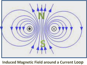
In 3D both forms of energy field generate a broad looped torus-like pattern around their respective poles (e.g. the lines of force around a dipole magnet and the energy field around a polarised bitron). Magnetic fields flow out from a North pole to return back via a South pole; electric fields have a divergent out-flow and a convergent in-flow poles. For both types of energy field their like-poles repel and opposite-poles attract. In this section we will take a closer look at the nature of these fields in order to provide an explanation of their attraction and repulsion characteristics.
The flow of electromagnetic energy within a magnetic field is from its North pole to its South pole: the energy flow has no circular component apart from its large arc trajectory around the magnet or current loop that generates it. Opposite pole attraction occurs because the magnetic out-flow (North) and in-flow (South) field lines energy join as shown in Figure 12(a) and Figure 12(b), and seek the shortest route possible: the in-flow of the South pole acts like a fishing reel pulling the North pole towards itself. Like-pole repulsion occurs because the energy flows push directly against each other in opposite directions as shown in Figure 12(c) for opposing North poles: the flowlines simply reverse for opposing South pole repulsion.
The mechanics of attraction and repulsion for electric fields are similar to those for magnetic fields, but involves fields with a circular flow component. But before considering the mechanics of attraction and repulsion between electric point charges, an explanation of attraction and repulsion between bitrons within bitron, e-, and p-strands is required.

Figure 12. Opposite-pole attraction and like-pole repulsion in magnets.
The circular spin of the neutral bitrons’ energy fields helps to jostle bitrons into like-spin compatible strand-like groupings. Within a strand-like grouping, low concentrations of energy accumulate between the bitrons as in Figure 13(a) and Figure 13(b). Each bitron is then competing for the available energy, drawing it towards the central hole of their core energy: it is the mutual competition for this energy that causes them to be pulled towards the resource-in-common (the blue arrows), so creating equal spacing between them.
When equally spaced aligned strand-like groups of bitrons are polarised the inner field energy flows from one bitron to the next, with an outer-return flow in the opposite direction as for the electrons in Figure 13(c). The field energy flows in opposite directions, with a combined flow twist in the same circular direction, serves to draw and keep them together, representing what we call attraction. Rotate 1 of the 2 electrons shown in Figure 13(c) by 180˚ and the inner, outer and circular flow components would all oppose each other to create what we call repulsion. The same applies to positrons, except that the circular rotation direction is reversed. Thus a pair of electrons, or a pair of positrons, can attract or repel each other depending on which way they are pointing.
An electric field is the combined outwardly directed fields of e- and p-strands. E-strands generate outwardly directed fields called e-wisp fields (or simply e-wisps) with an AO heading away from the negative pole associated with the negative side of an electric power source. P-strands similarly generate p-wisps with a CO heading from the positive side of an electric power source.
As well as AO e-wisps, a negative electric pole also generates AI p-wisps which are the tail-end of contained p-strands, which when connected to a CO headed p-wisp field from the positive pole form a p-thread field which transfers energy centrally from the positive to the negative pole (shown as the blue p-thread arrows of Figure 14). Similar connections form AO-to-CI e-threads which transfer energy from the negative to positive pole.

Figure 13. Polarised bitron strand energy flow.

Figure 14. Opposite charge attraction between monopole point charges.
The outer energy flows of p- and e-threads are in opposite directions and thus cancel each other out. Their inner energy flows are in opposite directions without interference, and together represent conventional electric field lines of force. Their circular energy field components are in the same direction and thus merge, and it is possible that the circular flow component may help to bend and connect wisps to form threads.
Attraction between electric poles of opposite charge is due to the pull of energy by e-threads (and thus the e-strands) on the negative pole, and the pull in the opposite direction by the p-threads on the positive pole. However conventional lines of force diagrams simply show an electric field moving inwards to a negative charge and outwards from a positive charge as in Figure 5(b) & Figure 5(c), which represent only the p-wisps and p-strands, which is only half the story. Figure 5(a) is a simpler version of the STEM approach that is visually closer to the conventional lines of force diagram.
Repulsion between like electric poles is due to wisps with the same heading clashing head-on, deflecting and pushing each other away: they also cancel out each other’s circular field component. The result is repulsion and the associated lines of force that are the same as for like magnetic pole repulsion; but electric attraction, as explained above, is distinctly different to magnetic attraction.

8. Capacitor Charge and Discharge
The dielectric material, as used in an electric capacitor, is an electric insulator that provides significantly more resistance to bitron movement than an electrical conductor. Also a dielectric contains smaller quantities of free bitrons than an electrical conductor. Although dielectric bitrons are sparse and bitron strands less densely packed and possibly more contorted, they can be polarised and become quite highly energised, and keep the acquired energy long after the charging energy source is turned off. Energy so stored can then be released as an electric current when the circuit is in discharge mode.
During the charge phase (Figure 15(a) and the circuit diagram of Figure 15(d)) polarised e- and p-strands within the circuit cannot enter the dielectric insulator, but instead become concentrated on the capacitor plate’s outer surface. The electric fields that have built up on the capacitor’s outer surfaces polarise neutral bitrons within the dielectric via induction, forming electrons on the negative side of the circuit and positrons on the positive side. These polarised bitrons slowly and laboriously work their way in opposite directions (the small arrows of Figure 15(a)) through the dielectric as a weak electric current that is internal to the dielectric.
Eventually the polarised bitrons within the dielectric have moved as far as they can towards their respective sides of the capacitor and cannot absorb any more energy: the capacitor has thus reached full capacity. However because the dielectric bitrons are so few in number compared with those available in the wire conductor of charging circuit, they accumulate significantly more energy than their counterparts in the open charging circuit: enough energy so that they do not revert back to neutral bitrons when the charging circuit is turned off. This is most important for the discharge phase.

Figure 15. Electric capacitor charge and discharge phases.
For the discharge phase, the charging power supply is switched out as in Figure 15(e) and the charged capacitor becomes the new power source. The removal of the charging power source causes all the polarised strands in the charging circuit to instantly revert back to being neutral strands (see Figure 15(b)); but not so for the highly energised polarised bitrons within the dielectric. The electric fields of the polarised bitrons that have accumulated along the outer surface of the dielectric now induce the polarisation of the newly neutral strands in the wire conductor, transforming them into polarised strands.
The electrons that have accumulated on what was the positive side during the charge phase now induce neutral strands within that side of the conductor to polarise and form e-strands, which then represents an electron supply situation. Thus the once positive side of the circuit has been converted into a negative terminal.
The reverse happens on the other side of the capacitor, creating a positive terminal. Thus a new source-sink electric potential has been created, and an electric current flows in the opposite direction to the charging current as shown in Figure 15(c) and Figure 15(e). Eventually the dielectric strands lose energy and revert to their neutral state, and the capacitor power is exhausted and so the discharge current flow stops.
Interestingly, the Wikipedia definition for a dielectric is “an electrical insulator that can be polarised by an applied electric field”, and the explanatory diagram provided for “dielectric polarisation” (duplicated as Figure 15(f)) involves the use of electric dipoles, which are incompatible with the concept of ONAM’s monopole electric charges, to explain the phenomenon. In a similar vein, the creative use of fictional positive holes to explain semiconductor charge transfer provides another example of conventional Science’s dilemma with trying to explain electricity. STEM, on the other hand, does not require any such adjustment or compromise, as all the subtleties of electricity and magnetism are fully accounted by the model.
9. Superconductivity
So far this paper has suggested that the electron and positron strands are continuous from source to sink, but this is far from the case. In temperatures above about 170 K, even the best of electrical conductors (e.g. Au) are far from perfect conductors: structural flaws (crystal interfaces and micro-fractures associated with the manufacturing process) and contaminants ensure that is the case. Structural flaws and contaminants provide barriers that can break strands into smaller strands. Broken strands can usually re-connect with other strands to build into longer strands, but the process of bending, breaking and (re)joining strands creates energy loss in the form of heat and light. The electromagnetic fields of atoms of the carrier also push and pull on the strands, impeding their movement. It is the amount of difficulty encountered by strands moving towards their respective sinks that determines a carrier’s resistance (Ω).
Usually when a metal conductor is cooled there is an increase in conductivity. STEM contends that cooling, and super cooling in particular, involves the loss of energy by the atoms of the conductor rather than the loss of energy of the free electrons and positrons within strands. Energy losses of atoms within the conductor reduce the strength of their electromagnetic fields which increases conductivity accordingly.
Superconductivity for superconductive materials commences at about 170 K (164 K, under 30 GPa of pressure for HgBa2Ca2Cu3O8+x). The electromagnetic barriers presented by atoms in the superconductor, including contaminants, are minimised as the temperature approaches the conductor’s Critical Temperature. When a current is applied the electron/positron strands connect for the full length of the conductor without break, virtually unimpeded by atom and contaminant electromagnetic fields, turning it into a perfect conductor. In superconductor mode virtually no energy is lost negotiating barriers to strand movement and the energy flow outside the strands is so strong that the magnetic flux from external magnetic fields is excluded. Even after the power source is removed, the electromagnetic fields of the conductor atoms are so weak that the free electrons and positrons within strands keep most of their axial alignment to display perfect diamagnetism (the Meissner Effect).
10. Free Electron and Positron Farming
Electrons are most commonly sourced from thermionic cathode ray tubes (e.g. first generation TV tubes): those used in research settings are usually called electron guns. Unfortunately, by reversing the anodes and cathodes of electron guns does not create a Positron gun (it more readily becomes a proton gun) because positrons require much more energy in order to be ejected from matter as free positrons.
Low level concentrations of positrons can be sourced from to Beta+ decay and Electron Capture. One practical application of this source is Positron Emission Tomography (PET). PET is a gamma imaging technique using radionuclide tracers that generate positrons which trigger electron-positron annihilation inside a patient’s body: the resulting pair of gamma ray travel in opposite directions, and are detected allowing the tracer locations to be accurately mapped producing a high resolution image.
Although electrons and positrons can easily be manipulated and concentrated (e.g. a Van de Graaff generator or simply rubbing a synthetic cloth against a glass or perspex rod), it is difficult to generate larger quantities of free positrons outside their host medium.
One brute-force technique for generating useful quantities of free positons is to bombard a metal film with high kinetic-energy electrons so as to knock positrons out of the metal film. At CERN, the LIL (Large Scale Electron-Positron Collider Injector Linac) uses an electron gun to assemble electrons with energy of 80 keV; these are in turn accelerated to energy of around 200 MeV which are then shot at a tungsten target to produce positrons that can be magnetically separated and further accelerated for particle collision purposes. This is an expensive, larger-scale operation of limited availability to a small handful of researchers.
On a smaller scale, a positron beam was generated 2013 [13] using a laser-driven particle acceleration setup (see Figure 16). A petawatt (1015 W) laser was fired at a sample of inert helium gas, creating a stream of electrons moving at very high speed, which were directed at a very thin sheet of metal foil: the resulting collisions produced a stream of electron and positron (and gamma ray) emissions which could be separated using magnets. This has led to cheaper, more practical setup options for researchers.

Figure 16. Laser setup for electron and positron generation.
11. Atomic Structure, Chemical Reactions, EMR and Gravity
STEM is not restricted to the definition of electrons, positrons, electromagnetic fields and electricity. It can be extended to define a structure Preons, quarks [14] and nucleons and to explore the nuclear structure of atoms (see [12] ), and to provide explanations for the physical characteristics and different allotropic forms of elements in the Periodic Table; their various bonding geometries; and for electron capture and beta decay.
STEM can also provide feasible explanations for the particle-wave nature of EMR, spectral line emission and absorption, the photo-electric effect, the Compton effect, electron pair generation and annihilation, and Gravity (see [15] ).
12. Summary and Conclusions
Good electrical conductors contain abundant neutral bitrons, orientated so that half spin clockwise and the other half anti-clockwise, with like-spin bitrons self-organising into linear groups called strands. STEM contends that electricity is the two-way movement of strands polarised with the same circular spin direction but different chirality: it thus involves only half of the bitron strands. Of these, half are electron strands (e-strands) and the other half are positron strands (p-strands).
The helicity of the polarised strands’ outer energy fields causes them to push against the neutral strands and so move; but due to their opposite chirality, they move in opposite directions as positrons and electrons. Such movement results in an electric current with e-strands moving towards the positive terminal (physical or implied), leading with their AO poles, and p-strands towards the negative terminal, leading with their CO poles. Because the polarised strands all have the same spin direction, their outer energy fields combine to produce an induced circular magnetic field around the wire conductor through which they move.
An electric field, such as generated by attaching a probe to the appropriate terminal of an electric power source, is formed by the combined energy fields of polarised bitron strands that extend beyond the outer surface of the probes. The lines of force associated with electric fields are extensions of polarised bitron strands, and thus have a circular spin component which distinguishes them from the lines of flux associated with a magnetic field, which have no spin component. Both electric and magnetic fields consist of exactly the same type of energy but they have different flow patterns.
Apart from having different chirality, electrons and positrons have the same structure and electromagnetic characteristics. Extracted (or farmed) positrons are easily identified and separated from electrons using a magnetic field, but when within a solid host material, they are most difficult to distinguish from electrons. Although low levels of positrons are a bi-product of pair production and Beta radiation, because positrons require considerably more energy to allow them to escape a host medium than do electrons, elaborate high energy accelerators are required to extract useful quantities of free positrons. Such technologies (e.g. the desk-top positron generator [16] ) have only become available over the past 10 years or so, and thus it is easy to see how, historically, the presence of positrons in material (such as electrical conductors) has been missed.
The Orbital Nuclear Atomic Model (ONAM), which is based upon a point-form monopole electric charge definition of the electron, does not and probably cannot support the concept of positrons within matter; and herein lies a major problem for Science. The ONAM approach considers that positive electric poles reflect a lack of orbital electrons and negative poles an excess of orbital electrons. It describes electric currents as the one-way movement of electrons from a negative pole to a positive pole (although there is uncertainty as to whether electric currents flow from positive to negative), and then relies on fictional positive holes, which are functionally the same as positrons, to explain semiconductor generated electric currents and fictional dipoles to explain capacitor charge and discharge.
STEM provides logical, consistent explanations regarding the nature of and interdependency between electric and magnetic fields; electrons; positrons; electric current flow; capacitor charge and discharge; the induction of electric current; and superconductivity. It represents a new and different approach that has the potential to cause a major re-think about electricity: it is certainly radically different from the ONAM-based interpretation involving the one-way movement of negatively charged monopole electrons.
The future ramifications of STEM for Science, industry and education are significant, and extend far beyond electricity. The presence of both free electrons and positrons within matter opens a large can of worms requiring a re-think about atomic structure [12] , ionic bonding, chemical reactions, EMR [15] , and Gravity. They are all connected, and electricity is just the start.
Acknowledgements
Thanks to Professor Ian McArthur, University of Western Australia who provided much appreciated technical advice and mentoring in the early stages of the development of STEM.

Conflicts of Interest
The author declares no conflicts of interest regarding the publication of this paper.
Cite this paper
Johnson, D. (2019) The Spin Torus Energy Model and Electricity. Open Journal of Applied Sciences, 9, 451-479. https://doi.org/10.4236/ojapps.2019.96037
References
- 1. Cambier, J. and Micheletti, D. (2000) Theoretical Analysis of the Electron Spiral Toroid Concept.
- 2. Consa, O. (2018) Helical Solenoid Model of the Electron. Progress in Physics, 14, 80-89.
- 3. Consa, O. (2018) The Helicon—A New Preon Model. Progress in Physics, 14, 215-219.
- 4. Bergman, D.L. and Wesley, J.P. (2002) Spinning Charged Ring Model of Electron Yielding Anomalous Magnetic Moment. Common Sense Science, 1, 63-67.
- 5. Kanarev, P. (2012) Particle Resolution. Proceedings of the NPA, Albuquerque.
- 6. Kyriakos, A. (2004) Geometrical Illustration of the Electromagnetic Representation of Dirac’s Electron Theory. ArXiv: quant-ph/0407071v1.
- 7. Wayte, R. (2010) A Model of the Electron. Progress in Theoretical Physics.
- 8. Williamson, J. and Van der Mark, M. (1997) Is the Electron a Photon with Toroidal Topology? Annales de la Fondation Louis de Broglie, 22, 133.
- 9. Osmera, P. (2012) Fractal Dimension of Electron. Proceedings of MENDEL.
- 10. Yao, A. and Padgett, M. (2012) Orbital Angular Momentum: Origins, Behavior and Applications. Advances in Optics and Photonics, 3, 161-204. https://doi.org/10.1364/AOP.3.000161
- 11. Lapoint, D.A. The Primer Fields/Experiments. http://www.rexresearch.com/lapoint/lapoint.htm
- 12. Johnson, D. (2019) Redefining the Electron—The Implications for Atomic Structure. Physics Vixra: 1904.0233.
- 13. Bostick, W. (1991) Mass, Charge and Current: The Essence and Morphology. Physics Essays, 4, 45-59.
- 14. Lincoln, D. (2012) The Inner Life of Quarks. Scientific American. https://doi.org/10.1038/scientificamerican1112-36
- 15. Johnson, D. (2019) Redefining the Electron—The Implications for EMR and Gravity. Physics Vixra: 1904.0332.
- 16. Sarri, G., et al. (2013) Table-Top Laser-Based Source of Femtosecond, Collimated, Ultra-relativistic Positron Beams. Physical Review Letters, 110, Article ID: 255002. https://doi.org/10.1103/PhysRevLett.110.255002
NOTES
1An alternative description is that the centripetal force provided by the ductile strength of the core energy is exceeded.
2A chiral object cannot be orientated to be superimposable upon its own mirror image.