Open Journal of Inorganic Non-metallic Materials
Vol. 3 No. 3 (2013) , Article ID: 34562 , 8 pages DOI:10.4236/ojinm.2013.33006
Photoelectric Properties of Crystalline and Glassy PbGeS3
1Uzhgorod National University, Department of Physics, Uzhgorod, Ukraine
2Мukachevo State University, Мukachevo, Ukraine
Email: crystal_lab457@yahoo.com
Copyright © 2013 Dmytro Ivanovych Bletskan, Vasyl Mykolaiovych Kabatsii. This is an open access article distributed under the Creative Commons Attribution License, which permits unrestricted use, distribution, and reproduction in any medium, provided the original work is properly cited.
Received March 14, 2013; revised April 12, 2013; accepted April 26, 2013
Keywords: Semiconductors; Chalcogenide glasses; Photoconductivity
ABSTRACT
The integrated investigations of the stationary characteristics of photoconductivity (the spectral distribution of photoconductivity (PC), luminous-ampere characteristics (LAC), temperature dependences of dark photoconductivity) and the thermostimulated current (TSC) for crystalline and glassy lead thiogermanate (PbGeS3) were performed. It was determined, as a function of crystals growing rate, there are one or two impurity maxima except for the native one in photoconductivity spectra. For the glassy lead thiogermanate in the range of wave lengths of 0.4 - 1.0 μm in PC spectra was revealed the hysteresis at the change of direction wave lengths sweep of incident light, conditioned by the phenomenon of induced impurity conductivity. The activation of PC, caused by thermal emptying of attachment levels, was observed on the temperature dependences of photoconductivity.
1. Introduction
Currently, the electronic properties of chalcogenide glassy semiconductors (CGS) and the role of localized states in their mobility gap are intensively investigated [1]. It should be noted that among the different research methods of CGS electronic properties an important place is occupied by the stationary and kinetic properties of photoconductivity (PC). Thus, the comparison of information is expedient for CGS and their crystalline analogues. However, such researches were executed only for the limited circle of objects, like as binary glasses and crystals GeSe2 [2-4], As2S3 and As2Se3 [5-7]. Therefore, there is not an united view of these phenomena mechanisms and microscopy of centers, accountable for the photosensitivity. The present information about the nonequilibrium electronic processes in chalcogenide glassy semiconductors it is desirable to complement of information, obtained on more difficult objects to which belongs also lead thiogermanate (PbGeS3). Its investigations are sparse, nevertheless it was determined that lead in PbGeS3 compound reveals the valency of two [8], in glasses of Ge-Pb-S ternary system is exposed the bimolecular recombination, the bipolar photoconductivity [9, 10] and quasi-discrete character of localized states distribution in the mobility gap [11]. Ge-Pb-S glasses are also X-ray sensitive and do not yield on basic parameters Se and PbO ones, used in X-ray vidicons [12]. The crystalline structure of lead thiogermanate is described in [13,14], the IR and Raman spectra of the ordered and disordered phases were investigated in [15-17], and the results of the detailed researches of the absorption edge in a wide range of temperatures are described in [18,19]. From the practical point of view the interest to ternary glasses of Ge-Pb-S system is conditioned by the wide possibilities to use them as the volumetric optical coating for the active devices of integral optics and multifunction devices of semiconductor photonics [20], also as the electrophotographic layers, characterized by substantially smaller (in two times) sizes of maximum charging potentials, and more rapid kinetics of dark semidecay that analogical layers, created on the base of As-S(Se) binary glasses [21].
In the present work the results of integrated investigations of the stationary characteristics of photoconductivity (the spectral distribution of PC, luminous-ampere characteristics (LAC), temperature dependences of photoconductivity) for the ordered (crystalline) and disordered (glassy) phases of lead thiogermanate are presented.
2. Experimental
The polycrystalline working mixture of PbGeS3 has obtained by a joint meltback of the initial elements taken in stoichiometrical ratio in the vacuum quartz ampoules (~ 10–3 Pа) at heating to the temperatures ~1200 K using the vibration stirring. Sulphur, used for synthesis, subjected to additional purification by the vacuum distillation. PbGeS3 single crystals have grown by the directional crystallization of a fusion (it is the vertical variant of Bridgman technique). It is important at the growing of PbGeS3 crystals the production, close to stoichiometry, of homogeneous and perfect crystals, while the presence of volatile component (sulphur) in their composition remains the main source of high concentration of native point defects. A temperature gradient in the crystallization zone was 20 - 30 K/cm, drawing rate in the first case - 0.13 mm/h, in the second one –0.4 mm/h. Crystals had the appearance of cylinder of 18 - 20 mm diameter and till 60 mm long and easily split off on the cleavage plane. These crystals had a monoclinic structure with lattice parameters which corresponded PbGeS3 compound according to X-ray analysis data [13]. With the purpose to obtain glasses, the fusions of general mass of 8 - 10 g cooled down with the rate ~17 K/s. Microstructural and X-ray analyses demonstrated that all glasses had been homogeneous and not contained the crystalline inclusions.
For the measuring of photoconductivity on the native surfaces (001) of investigated samples, broken off from the bulk crystal, aquadag or indium contacts were sprayed. The last ones were created by thermal evaporation in vacuum. The investigations of PC spectra were performed in the range of wave lengths 0.4 - 2.0 μm at the illumination of samples by monochromatic emission in the condition of electrostatic field. Chosen intensity of monochromatic light always was such, that during measurements the luminous-ampere characteristic Iph = f(L) remained linear in all range of investigated wave lengths. Current in a chain had measured by direct-current amplifier.
3. Results and Discussion
3.1. The Conductivity on a Direct Current
The dark specific conductivity of crystals is (5 - 9)·10–13 Ω–1·сm–1 at Т = 293 K. It is known, that wide-gap crystals with low concentration of charge carriers possess in a varying degree of donor and acceptor centers compensation. Indeed, the presence in PbGeS3 ternary crystals two types of the cationic sublattices and volatile sulphur stimulates the generation of variety of native point defects, mainly due to the deviation from the stoichiometry. In consequence of that, native point defects of both donor and acceptor types can be simultaneously created during the growing process, i.e. there would be auto compensation what forms the semiinsulating crystals.
The temperature dependence of the crystal dark conductivity (Figure 1, curve 1) is described by characteristic exponential law for the impurity compensated semiconductors:
sт = soexp(Еа/kТ) (1).
with the activation energy Ea = 1.12 ± 0.05 eV.
The transition crystal-glass in lead thiogermanate, similarly to other typical glass formers, for example As2S3 and GeSe2 [13], is accompanied by diminishing of the conductivity in one-two order of magnitude. Taking into account that the short-range order in crystalline and glassy phases is identical [15], the change of conductivity is conditioned by the disappearance of the long-range order. The temperature dependence of the dark conductivity for the glass (Figure 2, curve 1), as well as in the case of the crystal, is described by the exponential dependence (1) with the unique activation energy Еа = 0.91 eV. According to [22], it is possible to judge about the
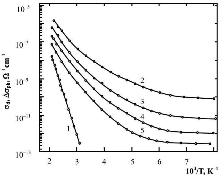
Figure 1. Temperature dependences of the dark conductivity (1) and PC of PbGeS3 crystal at different illuminations L, lux: 2 - 104; 3 - 2.5 × 10³; 4 - 6.25 × 10², 5 - 1.56 × 10².
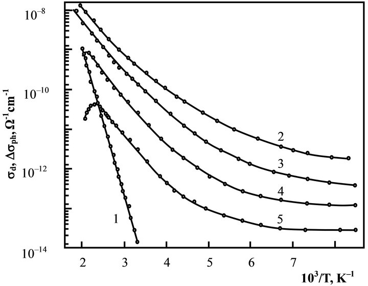
Figure 2. Temperature dependences of the dark conductivity (1) and PC of PbGeS3 glass at different illuminations L, lux: 2 - 104; 3 - 2.5 × 10³; 4 - 6.25 × 10², 5 - 1.56 × 10².
mechanism of chalcogenide glassy semiconductors conductivity on a direct-current, taking into account s0 preexponential factor value in the expression (1). This factor was derived by the extrapolation of lnsт = f(1/T) line to T = ∞. The constant s0 is within the range 102 - 103 Ω–1·сm–1 for examined glasses. Such magnitudes of preexponential factor value are characteristic for the conductivity, related to the carriers that excited in the localized states and located in the tails of allowed bands.
3.2. Photoconductivity Spectra
Crystals and glasses of PbGeS3 compound are photosensitive without special doping and additional heat treatment. The photoresponse ratio to the integral light with illuminance of L = 104 lux K = sL/sD (where sL—daylight conductivity) is 102 - 103 for crystals and 101 - 102 for glasses, taken from different lots of synthesis.
The polarized photoconductivity spectra of PbGeS3 crystal, grown at 0.13 mm/h interface velocity, are presented on Figure 3 (curves 1, 2). It can see at the comparison them to edge absorption spectra for the proper polarizations (curves 4, 5) that the high-energy maximum of photoconductivity hvmax1 = 2.57 eV in polarization of E||b is in the range of fundamental absorption edge and consequently conditioned by proper zone-zone transitions. The proper maximum of PC is moved to the lowenergy region of hvmax2 = 2.54 eV symbatically to the self-absorption edge shift at Е||с polarization.
Our previous measuring [19] of polarized spectra of crystalline PbGeS3 absorption edge in the range of fundamental absorption (2.5 - 3 eV) and the temperature
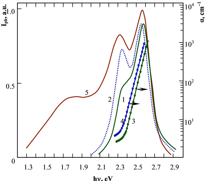
Figure 3. Polarized spectra of photoconductivity (curves 1, 2) and edge absorption (3, 4) of PbGeS3 crystal, grown at u = 0.13 mm/h for E||b (1, 3) and E||c (2, 4) polarizations. Curve 5—nonpolarized PC spectrum for crystal, grown at u = 0.4 mm/h, T = 293 K.
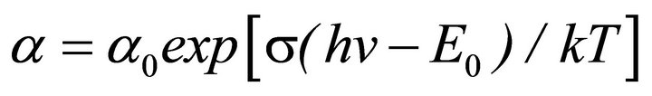
interval 70 - 300 K showed that in both polarizations E||b and E||c the types of absorption are described well by the Urbach rule
 .
.
thus, the dependence of absorption coefficient a versus hn in the range of fundamental absorption edge at a £ 103 сm–3 is not radical as in the case of direct gap transitions in ideal semiconductors, but is exponential one with the temperature dependent slope. In this case, demonstrated by authors [23], the application of the Moss rule to determine the semiconductor bandgap by PC spectra is not really reasonably. In addition, the estimation of Eg value by PC spectra from the energy position of the proper photoconductivity long-wave edge is laboured by the fact that impurity bands in PbGeS3 crystals are strongly shown, and also they overlap with the proper band at high temperatures (Figure 3, curves 1 - 3). The effective width of bandgap will be certain with a high accuracy according to the energy position of proper maximum in the photoconductivity spectra of crystals with exponential dependence of long-wave absorption edge in the wide ranges of samples thicknesses and surface recombination rates [23]. Thus, if the transitions band energy to estimate according to the spectral position of photoconductivity proper maximum (Figure 3), the bandgap of crystalline PbGeS3 is Eg = 2.57 eV (Т = 293 K).
The presence of different sort of inhomogeneous in the crystals and related to them the potential relief, must substantially affects on their properties, and first of all on nonequilibrium ones, such as the photoconductivity. In the real PbGeS3 wide-gap crystals there are native point defects (the isolated interstitial positions, vacancies in the lattice sites, and also their complexes among themselves, statistical distributing of two sorts of atoms—cations on cationic positions—antistructural distribution) and impurity point defects (remaining uncontrolled impurities, caught in the crystal from initial substances at the synthesis of ternary compound), that forming the localized electron states in the bangap. The formation of varying point defects substantially depends on the method of crystal growing, also conditions of their production and the impurity composition of initial mixture. All of above factors have an effect on PC spectral distribution. Thus, the high-quality crystals are formed at the low growing rate (0.13 mm/h), and in the PC spectrum there is only one impurity band hvmax3 = 2.34 eV, except for the presence of proper maximum, which also possesses some polarization dependence (Figure 3, curves 1, 2). According to the proceeding described in [24], the longwave edge of impurity photoconductivity is the wave length, at which the photoconductivity falls to 0.1 value of the maximum of appropriate band, and this magnitude is Еimp = 2.16 eV. There is good agreement with the result of energy position of absorption impurity band, found out by authors [18] at the studying of long-wave part of absorption edge in PbGeS3 crystals in the range of values of absorption coefficient 30 < a < 50 сm–1. It is well known that impurity absorption, photoconductivity and photoluminescence are the processes, related to photoionization of any local levels in the bandgap, belongings not only to impurity atoms, but also to native defects of the different types of crystalline structure [25]. The increase of growing rate (0.4 mm/h) for PbGeS3 samples affects on the quality of crystals and general view of photoconductivity spectrum (Figure 3, curve 5). In particular, an insignificant displacement of the proper maximum takes place in the long-wave range of spectrum and it is the appearance of additional impurity band of photoconductivity at hvmax4 = 1.85 eV. Thus, the general view of PC spectrum of crystalline PbGeS3 depends on not only of compound atomic composition, but it is also the function of atoms ordering in the semiconductor of such difficult composition.
It is known that displacement of the fundamental absorption edge and accordingly the maximum of the proper photoconductivity to long-wave range observes in the case, when the different types of extensive defects (dislocations, grain boundaries) [26,27] present in crystals. These defects are the sources, arising up nearby them, of the electric and elastic tension fields. Taking into account these facts, it can suppose that in PbGeS3 crystals, grown at high rate, presents the inhomogeneous distribution of local deformation fields of compression and tension, which substantially change the spectrum of deep electronic states in bandgap and as the result the general view of PC spectrum. Therefore, it is possible to judge about quality of PbGeS3 crystals according to the general view of PC spectrum.
The spectral dependence of PbGeS3 photoconductivity is very sensible to the disappearance of long-range order at the crystal-glass transition. The PC spectra of glassy PbGeS3, measured at the different temperatures and different scanning directions of wave length of excitant radiation, are presented on Figure 4. The scanning direction influences both on the general view of PC spectrum and on the absolute value of photosensitivity (comparing curves 1 and 2, Figure 4). At the scanning of the wave length of exciting radiation in the direction of incident quantum energy increasing (IR ® UV from 1.0 to 3.0 eV) in the photoconductivity spectrum is observed the maximum at hvmax1 = 2.26 eV and arm ~ 2.0 eV on the long-wave decrease of baseband. The comparison spectra of photoconductivity and absorption edge, measured at the room temperature (Figure 4) shows, that the highenergy maximum hvmax1 = 2.26 eV in photoconductivity spectra of glassy PbGeS3 is in the range of exponen-
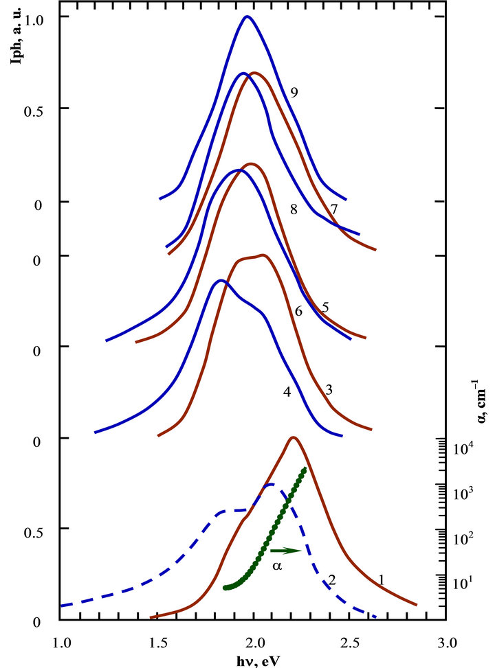
Figure 4. Photoconductivity spectra of glassy PbGeS3, measured at different scanning directions of wave length of incident monochromatic radiation: IR→ UV—curves 1, 3, 5, 7, 9; UV → IR—curves 2, 4, 6, 8, 9. Теmperature of sample Т, K: 1, 2—293; 3, 4—350; 5, 6—380; 7, 8—420; 9—470. Edge absorption a is at Т = 293 K.
tial edge of fundamental absorption and conditioned by zone-zone bipolar generation of free current carriers.
During the scanning of wave length of incident radiation, falling on the sample indirect UV ® IR (after its direct sweep), there is the redistribution of intensities in maxima of photoconductivity in favour of low-energy maximum with simultaneous displacement of high-energy one to the range of low energies (Figure 4, curve 2). This tendency becomes more expressed with the increase of temperature, so at T = 380 K the intensities of both maxima practically become equal. Whereas the low-energy maximum, with increasing temperature of sample, insignificantly displaces to the range of high energies, and the high-energy maximum on the contrary displaces to the range of low energies that leads to the situation when at the temperature of 470 K they practically overlap (Figure 4, curve 9). The form of PC spectra and energy position of maximum already independent to the scanning direction of wave length of excitant radiation at further heating of sample higher than T = 470 K.
If like the pseudobandgap width of glassy PbGeS3 to choose the energy, at which an exponential growth of the absorption coefficient a(hn) is completed, in this case Eg value, certain as an abscissa of the point in which a = 103 сm–1 (Figure 4, curve a), is 2.00 eV, that on 0.26 eV less than in the crystal. Thus, the vitrification of PbGeS3 compound, following by the disappearance of long-range order without the change of short-range one, results to the smearing of allowed bands edges and, as the result, to the disappearance of anisotropy and displacement of optical absorption edge, also the proper maximum in PC spectrum to long-wave spectral range.
It is possible to discuss the probable mechanism of hysteresis initiation in PC spectra of glassy PbGeS3. It is known that at the illumination of semiconductor there is not only the concentration change of free electrons and holes in the allowed bands, but also the change of filling by them the local impurity levels in bandgap, that can follow to the appearance of the induced impurity photoconductivity [25]. The last one consists in appearing or strongly increasing of the impurity photoconductivity in the semiconductor in which, at the normal state, the impurity conductivity absents or insignificant, after the preliminary illuminating of light with quantum energy hv ³ Eg. The induced impurity conductivity in high energygap semiconductors is observed in the case when in semiconductor bandgap there are attachment levels (t) for majority current carriers and trapping r-centers for minority ones. The attachment levels are filled of the majority current carriers, in the same time the minority ones, generated here, are trapped by r-centers and recombined at the preliminary illumination of sample by light of depth fundamental absorption range. If to illuminate such sample by impurity light, it would be absorbed by attachment levels, filled by the majority carriers that follow to the translation of last ones to the proper zone and to the appearance of induced impurity photoconductivity. Thus, transferred to the zone majority carriers than can either recombine or again return to the attachment levels. Obviously, the probability of the first process will be proportional the concentration of minority carriers, trapped by r-centers, and the probability of the second process depends on the concentration of unfilled attachment levels. Thus, the main condition of the appearance of induced impurity conductivity in the photoconductor is the presence in it the attachment levels, unfilled in dark. The study of Ge-Pb-S ternary glasses by the method of current thermostimulated depolarization (TSD) confirms the presence of two attachment levels in them [28].
Taking into account this fact, and also that the initially investigated PbGeS3 glassy sample was in the dark, and not of all attachment levels were fully, but only partly filled, therefore at the wave length scanning in IR ® UV direction the impurity conductivity shows up as the weak arm on the long-wave decrease of PC proper band (Figure 1, curve 1). The generation of electron-hole pair with the subsequent trapping of majority carriers (holes) on the attachment levels (Et) takes place at quantum energies hv ~ Eg. At the subsequent wave length scanning in reverse direction UV ® IR, except of band-to-band transitions, determining their proper PC maximum, there is the translation of electrons and holes from the prior filled attachment levels in u-zone. As a result, the induced impurity conductivity appears, that follows to the increase of intensity of impurity photoconductivity in the arm range (Figure 4, curve 2).
The determined character of photoconductivity spectrum transformation of glassy PbGeS3 versus temperature have no business to binary glass-forming compounds, such as As2Se3 or GeSe2, characterized by one type of base units. The similar dependence of photoconductivity spectra transformation is performed by us earlier for (GeS2)x(A2S3)1−x ternary glasses, where А = Bi, Sb [29].
3.3. Temperature Dependence of Photoconductivity
Assemblages of stationary photoconductivity temperature dependences (Dsph) of crystalline and glassy PbGeS3, measured at different light intensities L of sample by the proper absorption range light, are presented on Figures 1 and 2 (curves 2 - 4, accordingly). The change of intensity of incident radiation, falling on the sample, did not cause the substantial change of character of photoconductivity temperature dependence. There is the thermal activation of photoconductivity (TAP) for both phases with the temperature increasing. For glass, at least at low intensities of illumination, upon the completion of photoconductivity activation process, there is the temperature quenching of photoconductivity (TQP) (Figure 2, curve 5). The multiplicity of the temperature quenching is small (~10).
TAP and TQP effects related to the temperature dependence of lifetime of nonequilibrium charge carriers within the framework of the so-called multicentre recombination model, including the s-channel of intensive recombination, r-centers of photosensitivity and t-centers of attachment of majority nonequilibrium charge carriers in the most cases of high energy-gap crystalline semiconductors (and also in their glassy analogues) [30]. The role of t-centers consists in the determined (through the condition of electrical neutrality) the occupation of recombination centers. The depletion of t-levels results to TAP effect with the increase of temperature in this model.
The presence of one or two intensive impurity bands in PC spectra of PbGeS3 crystals indicates about the occurrence in them one ror two rand m-centers of slow recombination, acting the role of «sensitizing» centers. The results of measuring of thermostimulated current (TSC) in PbGeS3 crystals specify about the presence of attachment centers. There are three peaks on TSC curves at temperatures of 173, 227 and 290 K (Figure 5), which temperature positions of maxima weakly depend on the crystals growing rate. Here, it takes place only the intensity redistribution in maxima. TSC peaks displaced aside to the higher temperatures with the increase of heating rate and the amplitude of signal also grows. The slope of initial range of TSC curve is well described by expression I ~ . This fact allowed use for the determination of occurrence depth the method of initial current growth, developed by Garlick and Gibson [31]. Quasi-Fermi level coincides at the temperature of TSC peak with the attachment level, following Bube [24]. For the increase of precision of the determination of occurrence depth of attachment levels by the method of initial current growth the (temperature cleaning) of peaks was performed, in obedience to the scheme offered by Hoosgensraaten [32].
The experiment was carried out in the following way. For obtaining of TSC curve, the sample was cooled down in dark to 100 K, lighted up, after heated and then only the first peak was recorded. Further heating of the sample was stopped and it again quickly cooled down to the low temperature. After it heating was again launched and the second peak was recorded. Upon completion of the second peak record the heating process was again stopped and the sample sharply cooled down and the third peak was recorded. Separately TSC peaks were recorded during the second heating of the sample without it preliminary illumination. The occurrence energies of attachment levels, relatively to the top of valence band, equal to  = 0.21,
  = 0.44 and
  = 0.6 eV.
Investigations of the local states spectrum in the bandgap of ternary Pb-Ge-S glasses (for Ge28.5Pb15S56.5 compound) by the method of thermostimulated current depolarization measuring allowed authors [28] to reveal two maxima at temperatures 230 and 285 K, provided by
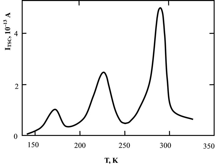
Figure 5. ТSC curve of PbGeS3 crystal.
the emptying of non-equilibrium filled trapping sites. The occurrence energies of two attachment levels relatively to the top of valence band in Ge28.5Pb15S56.5 glass:  = 0.2 - 0.3 eV (Тmax1 = 230 K),
 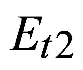 = 0.4 - 0.5 eV (Тmax2 = 285 K) were defined using the same method of the initial boost and step-by-step thermal refining of peaks [28]. It is clear, comparing the values of occurrence trapping levels depths in glass and crystal that in both phases the same attachment levels with close occurrence energies become apparent.
Thus, the recombination process in PbGeS3 crystals and glasses is substantially complicated by the attachment centers, the nonequilibrium occupation of which affects on the recombination centers filling and, as the result, on the stationary characteristics of photoconductivity. There is one wide peak on TSC curves in the case of glassy state.
Luminous-ampere characteristics Iph ~ Ln of crystalline and glassy PbGeS3, measured at two different temperatures showed on Figure 6. The numerical value of LAC index α was determined by specific mechanism of charge carriers recombination that used for its identification in practice. For both phases in the temperatures range, where takes place the temperature activating of photoconductivity, LAC is sublinear with the index n = 0.6 - 0.7. The sublinear increase of photoconductivity, observed in crystalline and glassy phases of PbGeS3 and also thermoactivation of PC with variable slope of Dspc(1/T) dependence, is characteristic for high energygap semiconductors with the presence in them large concentration of attachment centers distributed to energy.
Therefore, the stationary characteristics of photoconductivity of crystalline and glassy lead thiogermanate substantially depend on the lifetime of nonequilibrium charge carriers, which, in turn, determined by the dominant mechanisms of recombination in this temperature
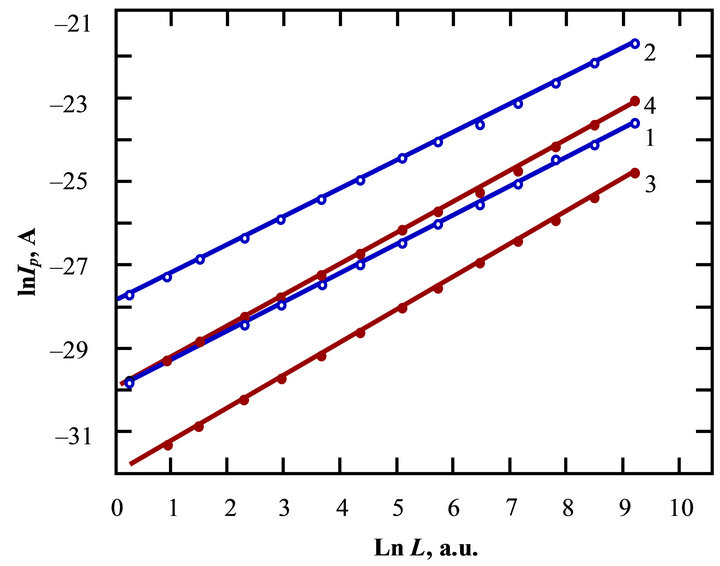
Figure 6. Luminous-ampere characteristics of crystalline (1, 2) and glassy (3, 4) PbGeS3, Т, K: 1, 3—293; 2, 4—370.
range. The observed activation of photoconductivity is not unique effect of the attachment of nonequilibrium charge carriers. It is only the partial reflection of more general process of local centers recharge at the excitation of crystal [30].
4. Conclusions
Thus, as the results of integrated investigations of direct current photoconductivity, stationary characteristics of photoconductivity, thermostimulated current and selfabsorption edge of crystalline and glassy lead thiogermanate phases it is determined that:
1) The disappearance of long-range order during the crystal-glass transition shows up in reduction of conductivity and band gap widths, also vanishing of anisotropy in PC and edge absorption spectra, that conditioned by smearing of allowed bands edges and the appearance of (tail) localized states because of the vitrification;
2) The similarity of photoconductivity and luminousampere characteristics temperature dependences, also the presence of the same bands in photoluminescence spectra and maxima on TSC and TSD curves, controlled by deep local levels in the gap of both phases and conditioned by the conservation of short-range order at the crystal-glass transition, and the uniformity of native defects of crystal and glass structures.
The distinctive feature of glassy PbGeS3, compared to crystals, there is the appearance of induced photoconductivity, arising after the preliminary illumination of sample by radiation of proper range, and related to it the hysteresis of PC spectra. Consequently, PbGeS3 glasses possess both stationary and induced photoconductivity.
REFERENCES
- C. D. Tsendin, “The Electronic Phenomena in Chalcogenide Glassy Semiconductors,” Nauka, St. Petersburg, 1996.
- D. I. Bletskan, N. V. Pоlazhinec and D. V. Chepur, “Photoelectric Properties of Crystalline and Glassy GeSe2,” Fizika I Tekhnika Poluprovodnikov, Vol. 18, No. 2, 1984, pp. 223-228.
- D. I. Bletskan, N. М. Krolevec and М. Yu. Sichka, “The Radiative Recombination of GeSex Glasses,” Fizika i Tekhnika Poluprovodnikov, Vol. 10, No. 10, 1976, pp. 1817-1820.
- V. А. Vasil’ev, Т. N. Mаmоntоvа and А. V. Chernyshev, “The Radiative Recombination Mechanism in the Glassy and Monocrystalline GeSe2,” Fizika i Tekhnika Poluprovodnikov, Vol. 24, No. 6, 1982, pp. 1769-1775.
- R. A. Street, “Luminescence in Amorphous Semiconductors,” Advances in Physics, Vol. 25, No. 4, 1976, pp. 397- 453. doi:10.1080/00018737600101412
- G. S. Higashi and M. Kastner, “Excitation-Energy Dependence of the Photoluminescence Total-Light Decay in Arsenic Chalcogenides,” Philosophical Magazine B, Vol. 47, No. 1, 1983, pp. 83-98. doi:10.1080/01418638308226786
- S. P. Depinna and B. C. Cavennelt, “Exciton and Pair Recombination in Crystalline and Amorphous As2Se3,” Philosophical Magazine B, Vol. 46, No. 1, 1982, pp. 71- 76. doi:10.1080/13642818208246423
- R. A. Castro, “Investigation of Impurity Atoms of Iron and Tin in Glassy Ge28.5Pb15S56.5 and Ge27Pb17Se56,” News of A.I. Gercen Russian State Pedagogical University, Vol. 6, No. 15, 2006, pp. 43-52.
- S. D. Baranovskii, G. A. Bordovsky, L. P. Kazakova, E. A. Lebedev, V. M. Lyubin and N. A. Savinova, “Bipolar Photoconductivity in Chalcogenide Glassy Semiconductors of Ge-Pb-S System,” Fizika i Tekhnika Poluprovodnikov, Vol. 18, 1984, pp. 1016-1020.
- G. A. Bordovsky, L. P. Kazakova, E. A. Lebedev., V. M. Lyubin and N. A. Savinova, “Ge-Pb-S Vireous Semiconductors with Bipolar Photoconductivity,” Journal of NonCrystalline Solids, Vol. 63, No. 3, 1984, pp. 415-418.
- G. A. Bordovsky, М. R. Kanychev and Т. V. Kanycheva, “Determination of the Density of States Function in CGS As2Se3 and Ge2.85Pb15.0S56.5 by Capacitance Spectroscopy Techniques,” Leningrad Saint Petersburg University, Leningrad, 1990, pp. 5-11.
- G. A. Bordovsky, V. M. Lyubin, N. A. Savinova and V. A. Svetickaya, “Photoand X-Ray-Conductivity in Thin Films CGS of Ge-Pb-S System,” Glassy Semiconductors, Leningrad, 2-4 October 1985, pp. 99-100.
- M. Ribes, J. Olivier-Fourcade, E. Philippot and M. Maurin, “Structure Cristalline d’un Thiogermanate de Plomb á Chaïnes Infinies (PbGeS3)n,” Acta Crystalographica B, Vol. 30, No. 6, 1974, pp. 1391-1395. doi:10.1107/S056774087400495X
- J. Sejkora, P. Berlepsch, E. Makovicky and T. Balić- Zunić, “Natural SnGeS3 from Radvanice near Trutnov (Czech Republic): Its Description, Crystal Structure Refinement and Solid Solution with PbGeS3,” European Journal of Mineralogy, Vol. 13, No. 4, 2001, pp. 791-800. doi:10.1127/0935-1221/2001/0013-0791
- D. I. Bletskan, V. N. Kabacij, T. A. Sakal and V. A. Stefanovych, “Structure and Vibrational Spectra of MIIAIVB3VI-Type Crystalline and Glassy Semiconductors,” Journal of Non-Crystalline Solids, Vol. 326-327, 2003, pp. 77-82. doi:10.1016/S0022-3093(03)00381-8
- Z. V. Popovič, “Infrared and Raman Spectra of PbGeS3,” Physica В, Vol. 119, No. 3, 1983, pp. 283-289.
- Z. V. Popovic, “The Vibrational Properties of Single Crystal PbGeS3,” Fizika Tverdogo Tela, Vol. 28, No. 2, 1986, pp. 344-351.
- U. V. Alpen, J. Fenner and E. Gmelin, “Semiconductors of Type MeIIMeIVS3,” Materials Research Bulletin, Vol. 10, No. 3, 1975, pp. 175-180. doi:10.1016/0025-5408(75)90152-X
- D. I. Bletskan, V. N. Kabacij, I. P. Studenyak and V. V. Frolova, “Edge Absorption Spectra of Crystalline and Glassy PbGeS3,” Optics and Spectroscopy, Vol. 103, No. 5, 2007, pp. 772-776. doi:10.1134/S0030400X0711015X
- D. I. Bletskan and V. N. Kabatsii, “Volumetric Optical Coating and Device for Its Infliction,” Patent of Ukraine No. 95127, Bul. 13, 2011.
- L. I. Bekicheva, G. A. Bordovsky, М. R. Kanychev, N. A. Savinova and V. V. Stepanov, “The Influence of Deep Trapping Levels on the Characteristics of Two-Layered Electrophotographic Information Carrier,” Journal of Scientific and Applied Photography and Cinematography, Vol. 32, No. 2, 1987, pp. 123-128.
- A. E. Owen, “Electron Transport in Chalcogenide Glasses, Coherence and Energy Transfer in Glasses,” Plenum, New York, 1984, pp. 243-278. doi:10.1007/978-1-4684-4733-0_11
- A. I. Vlasenko, Z. K. Vlasenko and A. V. Lyubchenko, “Spectral Characteristics of the Photoconductivity of Semiconductors with Exponential Edge of the Fundamental Absorption,” Fizika i Tekhnika Poluprovodnikov, Vol. 33, No. 11, 1999, pp. 1295-1299.
- R. H. Bube, “Photoconductivity of Solids,” Wiley, New York, 1960.
- S. M. Ryvkin, “Photoelectric Phenomena in Semiconductors,” Fizmatgiz, Moscow, 1963.
- H. F. Mataré and K. S. Cho, “Field Dependence of Photoresponse in Germanium Bicrystals,” Journal of Applied Physics, Vol. 36, No. 11, 1965, pp. 3427-3431. doi:10.1063/1.1703010
- W. Schröter, J. Kronewitz, U. Gnauert, F. Riedel and M. Seibt, “Bandlike and Localized States at Extended Defects in Silicon,” Physical Review B, Vol. 52, No. 19, 1995, pp. 13726-13729. doi:10.1103/PhysRevB.52.13726
- G. A. Bordovsky, М. R. Kanychev and V. M. Lyubin, “The Relaxation Process Features of the Surface Potential and Thermally Stimulated Effects in Bipolar Glassy Semiconductors of Ge-Pb-S System,” Fizika i Tekhnika Poluprovodnikov, Vol. 20, No. 9, 1986, pp. 1613-1616.
- D. I. Bletskan, V. N. Kabatsiy and V. V. Frolova, “Peculiarities of the Absorption Edge and Photoconductivity Spectra of (GeS2)x(Bi2S3)1−x Glasses,” Chalcogenide Letters, Vol. 4, No. 10, pp. 119-126.
- V. E. Lashkarev, А.В. Lyubchenko and M. C. Sheynkman, “Non-Equilibrium Processes in Photosemiconductors,” Naukova Dumka, Kiev, 1981.
- G. F. J. Garlick and A. F. Gibson, “The Electron Trap Mechanism of Luminescence in Sulfide and Silicate Phosphors,” Proceedings of the Physical Society, Vol. 60, No. 6, 1948, pp. 574-590. doi:10.1088/0959-5309/60/6/308
- W. Hoogensraaten, “Electron Traps in ZnS Phosphorus,” Philips Research Report, Vol. 13, 1958, pp. 515-693.