Detection
Vol.2 No.2(2014), Article ID:44730,6 pages DOI:10.4236/detection.2014.22003
Zener Phenomena in InGaAs/InAlAs/InP Avalanche Photodiodes
Dariusz Żak, Jarosław Jureńczyk*, Janusz Kaniewski
Institute of Electron Technology, Warsaw, Poland
Email: *jjurenczyk@ite.waw.pl
Copyright © 2014 by authors and Scientific Research Publishing Inc.
This work is licensed under the Creative Commons Attribution International License (CC BY).
http://creativecommons.org/licenses/by/4.0/


Received 1 March 2014; revised 2 April 2014; accepted 10 April 2014
ABSTRACT
Avalanche photodiodes are widely utilized in research, military and commercial applications which make them attractive for further development. In this paper the results of numerical simulations of uncooled InGaAs/InAlAs/InP based photodiodes are presented. The devices were optimized for 1.55 μm wavelength detection. For device modeling the APSYS Crosslight software was used. Simulated structure consists of separate absorption, charge and multiplication layers with undepleted absorption region and thin charge layer. Based on numerical calculations, the device characteristics like band diagram, dark current, photo current, gain, breakdown voltage and gain bandwidth product were evaluated. The simulation results highlight importance of Zener effect in avalanche photodiode operation.
Keywords:Avalanche Photodiode, InGaAs, Modeling

1. Introduction
Avalanche photodiodes have been utilized in many applications when very low power and high frequency signal detection are the main requirements, e.g. laser range finding, optical radar systems, high sensitivity spectroscopy, fibre optic communication and many other applications [1] . Differing from a p-i-n photodiode, an avalanche photodiode (APD) is designed to own internal gain, which originates from the carrier impact ionization and occurs mainly in the high electric-field in intentionally undoped multiplication region. The main limitation for device performance is associated with multiplication noise arising at high gain operation region, which is directly related to ionization rates ratio for electron and holes. In contrast to silicon, majority of AIIIBV compounds are characterized by small carriers ionization rates ratio which leads to lower performance due to high multiplication noise during avalanche process [2] [3] .
Simulations of semiconductor devices allow for deeper understanding of electrical and optical phenomena coexisting in the structure. It allows for architecture design with improved precision. Additionally device modeling is much cheaper than fabrication of semiconductor devices. Therefore highly advanced simulating software is constantly needed.
In this paper results of APD simulations are presented. SAGCM (Separated Absorption Grading Charge and Multiplication) photodiodes were analyzed by means of APSYS software [4] . Basic models used in simulations are as follows: model of Shockley-Read-Hall and Auger recombination, model of incomplete ionization, carrier statistic and carrier mobility model. Several carrier mobility assumptions can be considered, i.e. constant mobility, simplified field dependent mobility, field dependent mobility, III-V materials mobility and Poole-Frenkel mobility. Additionally in devices operating under reversed bias tunneling model corresponding with Zener effect is taken into account.
2. APSYS Software
Modern avalanche photodiodes are complex semiconductor devices, hence designing process has to be supported by extensive software simulation of electrical and optical properties [5] [6] . APSYS Crosslight is a general purpose simulating software which solves Poisson’s Equation (1) and electron/hole continuity Equations, (2), (3), using finite element method.
 (1)
(1)
 (2)
(2)
 (3)
(3)
where: V—the electrical potential, —the relative DC dielectric constant, n—the electron concentration, p— the hole concentration,
 —the shallow donor concentration,
 —the shallow acceptor concentration,
 — the occupancy of the donor level,
 —the occupancy of the acceptor level,
  and
and —the electron and the hole current respectively,
  and
and —the electron and the hole recombination rates per unit volume,
 — the optical generation rate,
  ,
,  , i
, i —the spontaneous, stimulated recombination rates and the Auger recombination rate per unit volume.
3. Simulated Structure
Simulated structure is a modification of conventional avalanche photodiode with separated absorption, charge, and multiplication regions [7] . Space separation of absorption and depleted regions reduce dark current by suppressing the avalanche process in absorbing layer. The schematic layer structure of the simulated photodiode is presented in Table 1. All layers are lattice matched to semi-insulating InP substrate.
4. Results and Discussion
Analysis of the band diagrams (Figure 1) can provide basic information about design correctness and device properties. Simulated dark and photo current-voltage characteristics are shown in the Figure 2. In the calculations the value of incident light power was equal to 5 W*cm−2 at 1.55 µm.
The multiplication region plays crucial role in device performance as it influences important parameters of the structure, such as: gain, multiplication noise and gain-bandwidth product. Analysis of the electron current flowing across the structure give a possibility to identify regions where the multiplication of carriers occurs.
In order to highlight the multiplication region, the electric field distribution at 100 gain is imposed on the calculated values of the electron current for different bias voltages (Figure 3).
Precise positioning of the separation layer between the absorption and the charge regions is responsible for tunneling current reduction at low bias levels.

Table 1. Schematic layer structure of the avalanche photodiode.
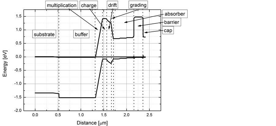
Figure 1. Band structure at equilibrium of the avalanche photodiode.
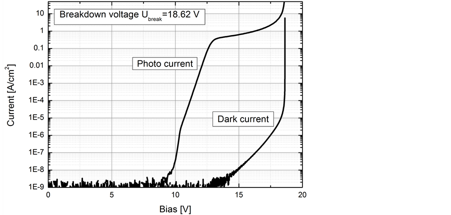
Figure 2. The current-voltage characteristics of the avalanche photodiode.
The absorption regions has been graded in three 150 nm steps, with different doping values to form quasi electric field which aids carrier transport from the absorbing region into the multiplication space. The simulated dark current I-V characteristics, for different doping levels in the charge region, are presented in Figure 4. Minimal value of the dark current has been obtained for charge region doping level equal to 4 × 1017 cm−3, where lower doping results in an increase of tunnelling current and decrease of the breakdown voltage. For higher doping levels the breakdown voltage decreases due to raise of the maximum electric field value in the multiplication layer at lower bias voltages.
Doping level of the charge region equal to 4 × 1017 cm−3 seems to be ideal compromise between low dark current and high breakdown voltage. The structure is very sensitive for doping accuracy and even small changes in doping level in the charge region cause significant reduction in device performance.
A 50 nm thick composition-graded InGaAlAs quaternary alloy is used to reduce both the abrupt conduction band barrier and the carrier (holes) accumulation at the In0.53Ga0.47As/In0.52Al0.48As heterojunction interface. In order to evaluate the device gain-bandwidth product, simulations of the structure at 10 ps long, 5 W/cm2 light pulses under different bias voltages have been performed, and the results are presented in Figure 5. The frequency for which signal amplitude drops by 3 dB has been calculated using Fast Fourier Transformation (FFT). The considered avalanche photodiode structure exhibits 165 GHz gain-bandwidth product.
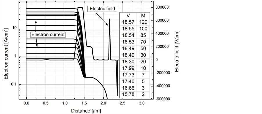
Figure 3. The electron current and electric field along the avalanche photodiode.
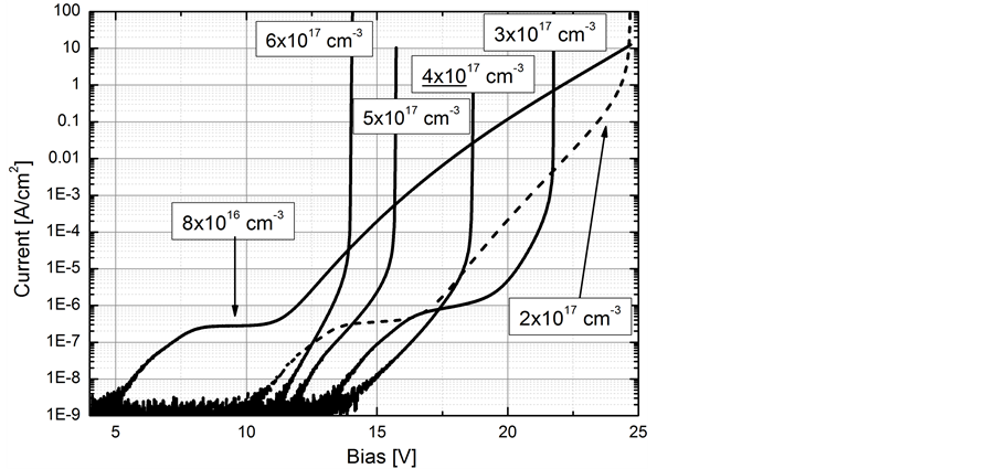
Figure 4. The dark current for different doping levels of charge region.
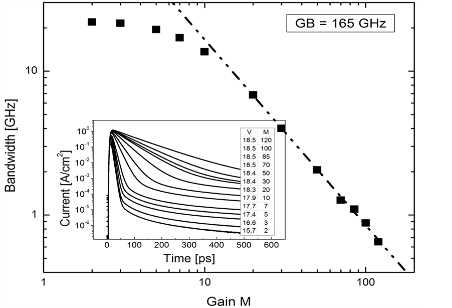
Figure 5. The current responses of the detector for the 10 ps pulse at different bias voltages and the bandwidth as function of gain.
5. Conclusion
In this paper the comprehensive APSYS modeling results of the avalanche photodiode structure, based on InGaAs/InAlAs/InP material system, have been presented. The Zener effect was taken into account in simulations, and had significant influence on the device properties, especially at low voltages. Basic device characteristics like band diagram, dark and photo current I-V characteristic, gain, breakdown voltage, multiplication noise and gain-bandwidth product were evaluated. The simulated structure is characterized by extremely low dark current and 165 GHz gain-bandwidth product. The optimal charge layer doping level is around 4 × 1017 cm−3 and has to be obtained with better than 1 × 1017 cm−3 doping precision.
Acknowledgements
This work was partially supported by The National Centre for Research and Development, Poland under project No N R02 0025 06.
The author acknowledges support from MPNS COST ACTION MP1204 - TERA-MIR Radiation: Materials, Generation, Detection and Applications.
References
- Campbell, C.J. (2007) Recent Advances in Telecommunications Avalanche Photodiodes. IEEE Journal of Lightwave Technology, 25, 109-121. http://dx.doi.org/10.1109/JLT.2006.888481
- McIntyre, R.J. (1966) Multiplication Noise in Uniform Avalanche Diodes. IEEE Transactions on Electron Devices, ED-13,164-168. http://dx.doi.org/10.1109/T-ED.1966.15651
- Yuan, P., Hansig, C.C., Anselm, A., Lenox, C.C., Nie, H., Holmels, L.A., Streetman, B.G. and Campbell, C.J. (2000) Impact Ionization Characteristics of III-V Semiconductors for a Wide Range of Multiplication Region Thickness. IEEE Journal of Quantum Electronics, 36, 198-204. http://dx.doi.org/10.1109/3.823466
- Crosslight Software Inc. http://www.crosslight.com/products/apsys.shtml
- Haralson, J.N., Parks, J.W., Brennan, K.F., Clark, W. and Tarof, L.E. (1997) Numerical Simulation of Avalanche Breakdown within InP-InGaAs SAGCM Standoff Avalanche Photodiodes. IEEE Journal of Lightwave Technology, 15, 2137-2140. http://dx.doi.org/10.1109/50.641534
- Xiao, Y.G., Li, Z.Q. and Simon Li, Z.M. (2007) Dynamic Drift-Diffusion Simulation of InP/InGaAs SAGCM APD. Physica Ststus Solidi (c), 4, 1641-1645. http://dx.doi.org/10.1002/pssc.200674253
- Li, N., Sidhu, R., Li, X., Feng, M., Zheng, X., Shuling, W., Karve, G., Demiguel, S., Holmes, A.L. and Campbell, C.J. (2007) InGaAs/InAlAs Avalanche Photodiode with Undepleted Absorber. Applied Physics Letters, 82, 2175-2177. http://dx.doi.org/10.1063/1.1559437
NOTES

*Corresponding author.