Open Journal of Acoustics
Vol.3 No.3A(2013), Article ID:36840,4 pages DOI:10.4236/oja.2013.33A002
The Influence of Ultrasonic Treatment on the Properties of Schottky Diodes
Physical Faculty, Chair of Physical Electronics, The Baku State University, Baku, Azerbaijan
Email: islam.pashayev@yandex.com
Copyright © 2013 I. G. Pashayev. This is an open access article distributed under the Creative Commons Attribution License, which permits unrestricted use, distribution, and reproduction in any medium, provided the original work is properly cited.
Received June 29, 2013; revised July 29, 2013; accepted August 6, 2013
Keywords: Photosensitivity; Barrier Properties; Amorphous Metals; Diodes Shottki; Superfluous Currents; Degradations; Ultrasonic Influence; Silicon Solar Elements
ABSTRACT
The given work studies the reason of the change of a superfluous current near crystallization temperature of an amorphous αPbSb metal alloy and at the same time founds out the influence of ultrasonic processing (USP) on the properties of αPbSb-nSi solar elements (SE), made by Shottki diodes technology (ShD) with a metal alloy. It is found that occurrence of a superfluous current αPbSb-nSi ShD under the influence of thermoannealing is connected with changes of structure of an amorphous film of metal at transition in a polycrystalline condition. VAC damaged αPbSb-nSi Sh Dare very sensitive to annealing time. Eventually, even at room temperature, level of a superfluous current decreases, i.e. “the wound” put by mechanical damage sort of heals, restoration process occurs the faster, the higher the annealing temperature is. Function of γt annealing parameters changes in an interval 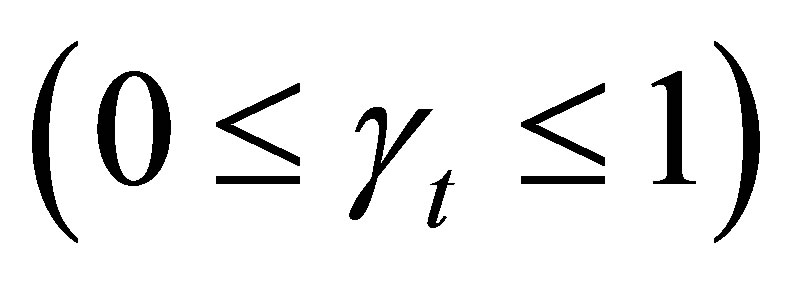 and the influence USP on photo-electric properties αPbSb-nSi SE depends on the chosen UIT mode.
1. Introduction
In the literature devoted to physics and technology of contact metal-semiconductor, the processes occurring in contact piece are extensively studied, and it is considered that all these processes are connected with the semiconductor. The role of metal in most cases is neglect. Influence of metals and their crystal structure on the processes which take place in contact piece, either is not considered, or is badly studied. To identify the role of metal ShD properties [1-4] have been studied. In late ХХ centuries, interest in ShD, made with application of films of metals and metal alloys with amorphous structure [2,4,5] has increased. The reason of such interest is that application metal films with amorphous structure allows to make ShD with important application properties. Advantage of application of amorphous metals also lies in the fact that due to the absence of granular structure and boundaries of grains in amorphous films a more homogeneous demarcation must be formed, and as effect of it, ShD should have properties, close to the ideal ones. Besides, there are messages that amorphous films of metals well play a role of diffusive and electric barriers in microelectronic structures. The present activity is devoted to studying of change of a superfluous current in a αPbSb-nSi ShD close to the temperature of crystallization of an amorphous metal alloy, and simultaneously to studying of influence of UIT on the properties of a αPbSb-nSi SE sample made on ShD technology with a metal alloy. In certain cases, under the influence of various factors, at low direct voltage superfluous current occurs in ShD there due to the degradation of the current-voltage characteristic [4,6]. In our experiment in αPbSb-nSi ShD the superfluous current appears at temperature near 573 К, as is shown in Figure 1. Along with temperature change structural changes take place [7] in amorphous metal films which appear at small direct voltage of VAC degradation. In this connection it is of interest to study degradation (superfluous currents) properties which have arisen under the influence of thermoannealing, and also study the influence of ultrasonic effect on photo-electric and electrophysical properties of semiconductor diodes and devices of this kind. Lately interest in a problem of purposeful change of physical properties of semiconductor materials does not weaken. Practically in all publications on this subject a question on particular gears of this effect remains unclear [8-12].
As ultrasonic effect is an effective mode of increasing
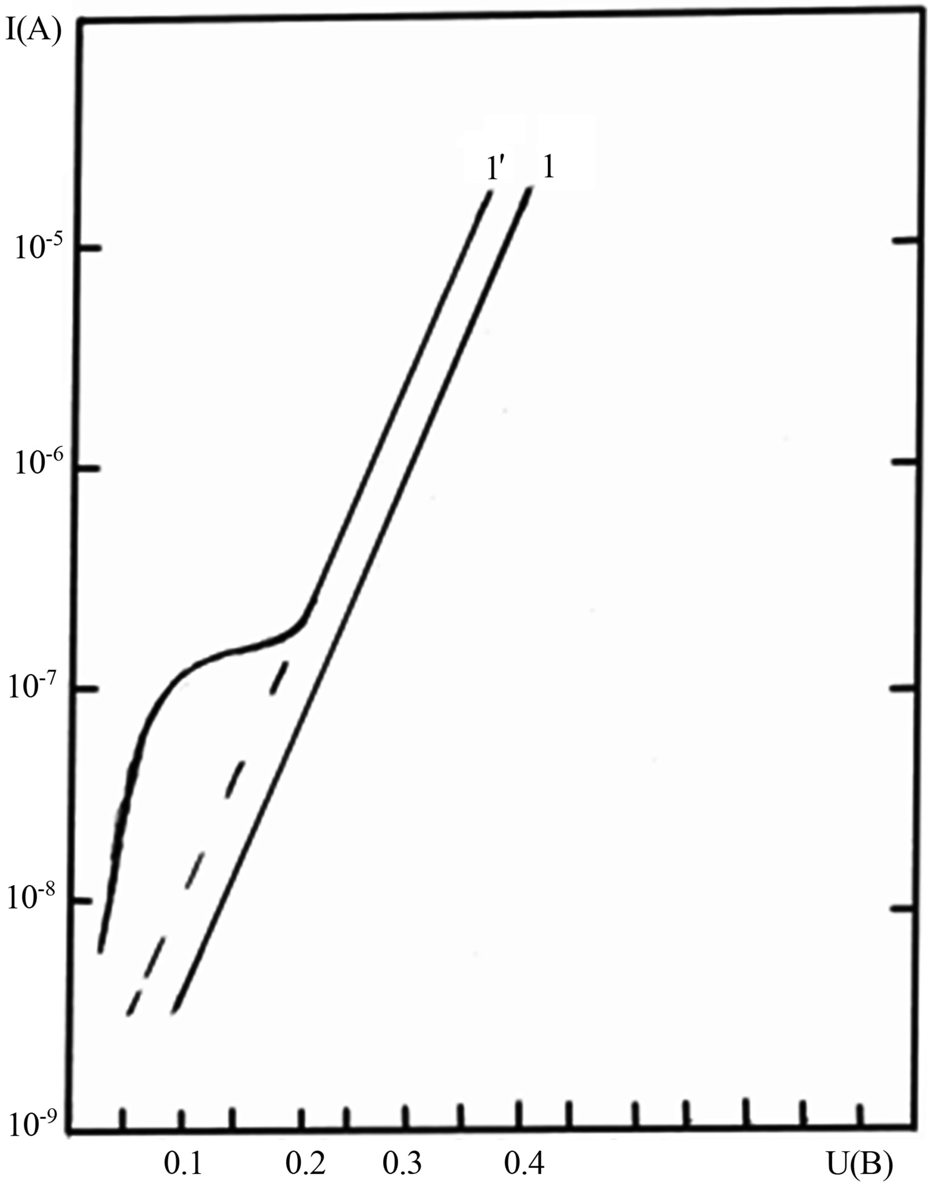
Figure 1. Current-voltage characteristic of αPbSb-nSi Shottki diodes 1-before and 1’-after a thermoannealing at 473 K.
the internal energy of solids, depending on absorption coefficient and intensity of ultrasound, various structural changes influencing both the photo-electric, electrophysical properties of materials and plastic deformation process are possible.
2. Experimental Process
For manufacturing a ShD a p-type silicon plate with orientation (III) and specific resistance of 0.7 Om·cm was used. The matrix contained 14 diodes which areas changed in the range from 100 to 1400 mkm2. The contact piece area in our case was equal to 300 mkm2. A αPbSb metal alloy was deposited by the method of electron beam evaporation from two sources. The αPbSb alloy has been chosen from those reasons that both components are widely applied in microelectronics, and the alloy is technological. A possibility of obtaining films of this alloy with amorphous structure was reported in paper [7]. The speeds of evaporation of components were chosen so that the film structure corresponded to alloy Pb52Sb48 as in paper [7] it was informed that such alloy is inclined to amorphization.
The thermoannealing of diodes was conducted at temperatures from 323 K to 573 K during identical periods of t = 10 minutes The structure of a film of an alloy before and after annealing was supervised by the radiographic analysis.
In Table 1, characteristics of αPbSb-nSi SE sample before and after UIT are presented at various modes. It is obvious from Table 1 that after UIT-1 (WUIT = 0.55 W/cm2, t = 200 min., fUIT = 25 MHz) the return current of the sample was increased by few times. The following stage of ultrasonic processing UIT-2 (WUIT = 0.15 W/cm2, t = 200 min., fUIT = 25 Mhz) has led to insignificant reduction of a return current. It, in our opinion, testifies the improvement of a defective condition of base SE. The subsequent stage of ultrasonic processing of sample UIT-3 (WUIT = 25 W/cm2, t = 90 minute, fUIT = 25 MHz) has one more time led to increase in a return current though after UIT with such power a breakdown of an SE or at least, increase of return current by few times was expected.
3. Results and Their Discussion
Figure 1 is presented current-voltage charachteristics for αPbSb-nSi ShD before and after annealing at 473 К. It is obvious from the schedule that after a thermoannealing at small direct voltages superfluous current appears. It is known that amorphous films of metals at certain temperatures change structure and turn into a polycrystalline state [7]. Hence, it is possible to assume that occurrence of a superfluous current in ShD after annealing at temperature of 473 K and above is connected with change of structure of a metal film of an alloy. Really, inspection of structure of Pb52Sb48 metal film on installation DRОН-2 before and after annealing at temperature 573 showed that the film of metal turns from an amorphous or quasiamorphous state into polycrystalline (Figure 2). As can be seen from the picture, the film of alloy Pb52Sb48 before annealing has amorphous structure. Such conclusion is made on such basis that crystals have a strongly featured series of maxima and minima, which indicates not only a correct arrangement of the nearest atoms, but also about existence of a distant order.
Figure 3 is presented the voltage-current characteristics for αPbSb-nSi ShD, degraded artificially by means
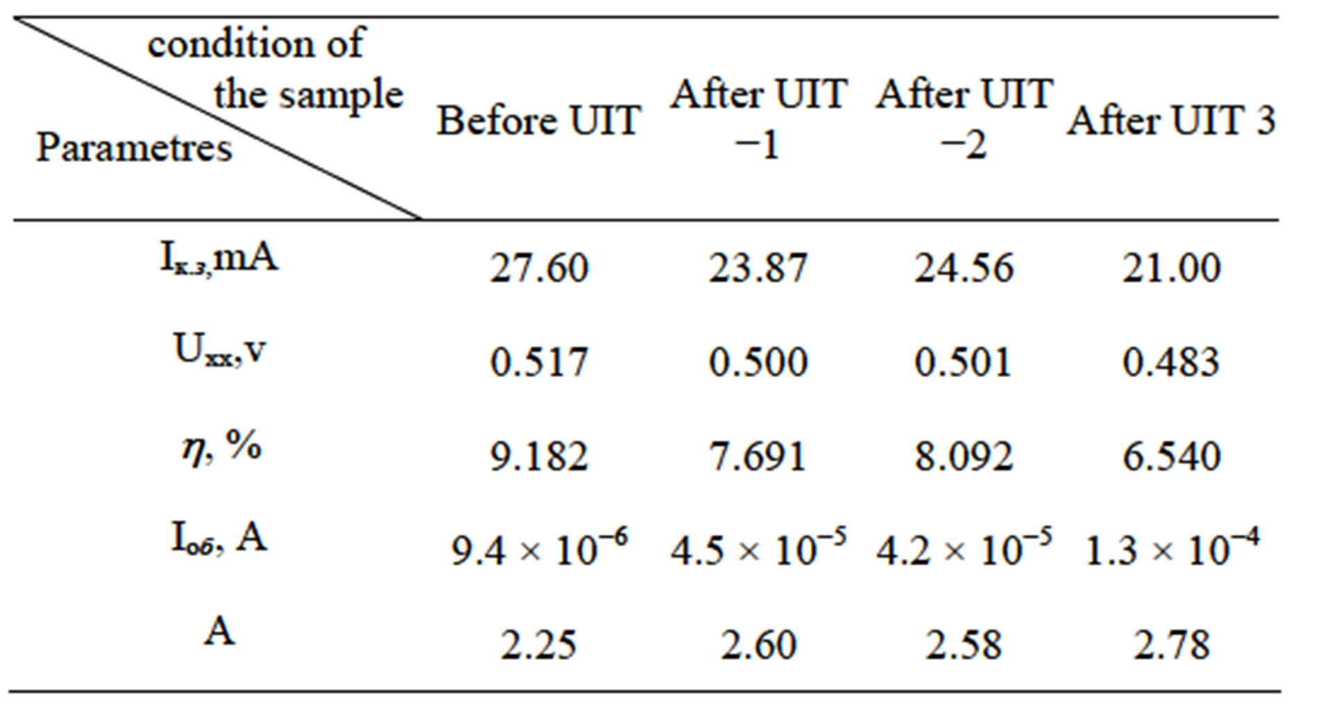
Table 1. Photo-electric parameters of αPbSb-nSi the sample before and after USP at R = 100 W/cm2 and Т = 300.
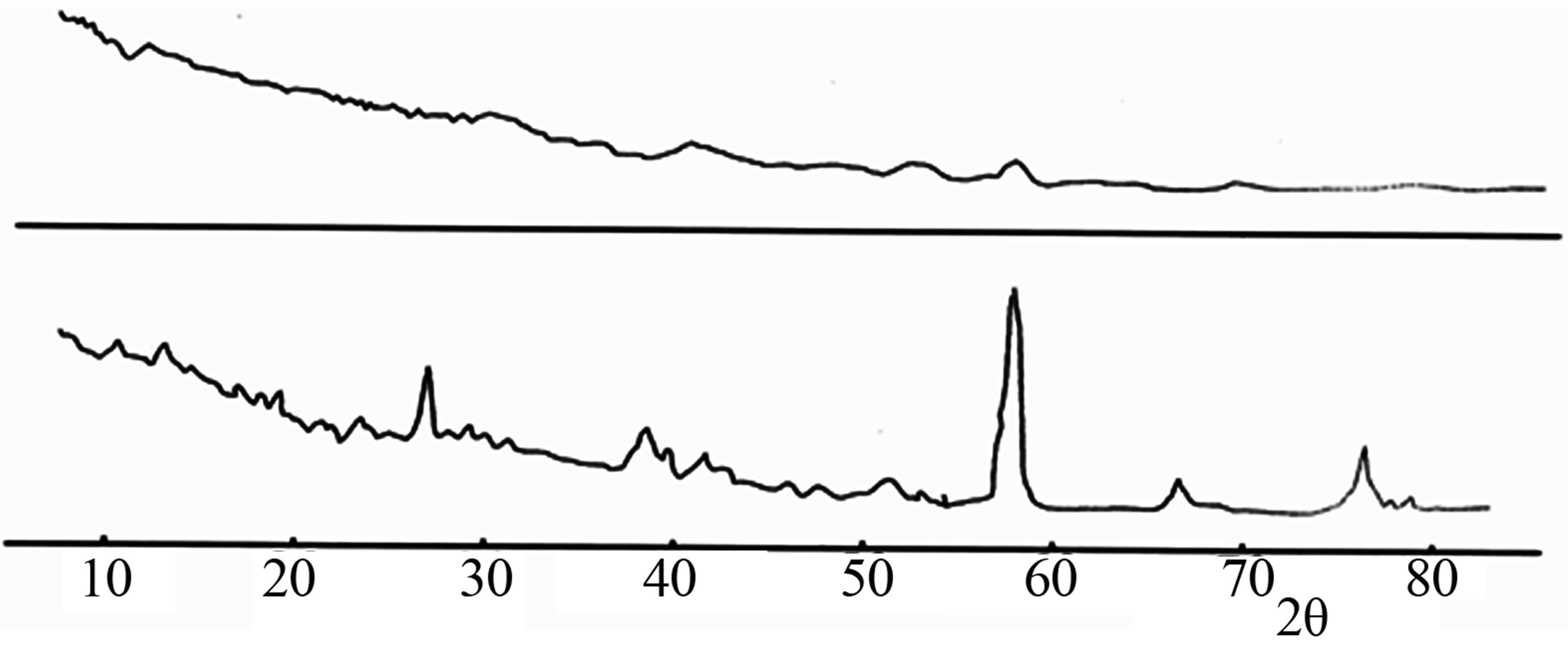
Figure 2. The X-ray structural analysis of amorphous metal films αPbSb. 1-to, 1’-after a thermoannealing at 473 K.
of a diamond hardometer PMT-3. The non-uniformity on border section BS was created artificially. The diamond needle of the adapter represents a correct quadrangular pyramid with a corner between opposite sides of 136˚. The area of the dislocated sections was varied by change of load value F (50 g) and quantities of violations N (1) before and after annealing at 473 К during some time: (1 - 17 s, 2 - 65 s, 3 - 148 s, 4 - 260 s, 5 - 410 s, 6 - 580 s, Vrev = 0.20). Degrading properties of αPbSb-nSi ShD after thermoannealing at temperatures from 323 К to 573 К were supervised by a method of removal currentvoltage characteristics both in forward direction, and return.
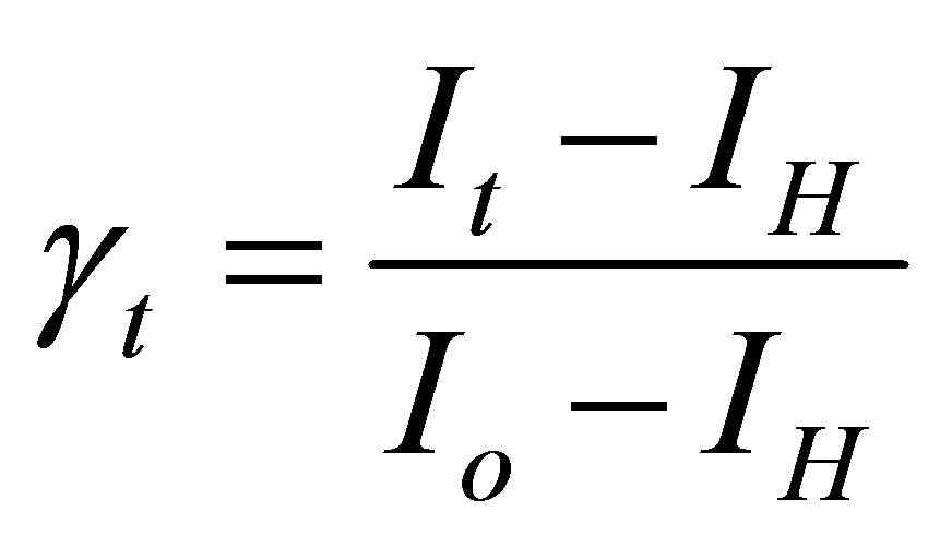
For the quantitative characteristic of recovery of a superfluous current under the influence of annealing, taking into account time, the following formula was applied:
where 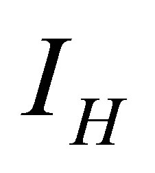 -current of a normal (intact) diodes Shottki,
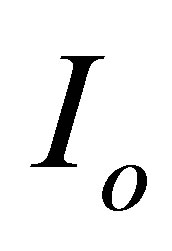 Diodes directly after influence if identer (
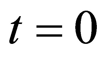 ),
),
 Damaged diodes, annealed during
  sec,
sec,
 Characterises relative recovery of a superfluous current under the influence of a thermoannealing during period t.
As is shown in Figuer 4, γt essentially depends both on Tann, and t. Value γt at various values of temperature of annealing and depending on t of annealing changes in an interval . From this it is seen that, first, the milestone of process of an annealing occurs for short initial periods, secondly, the milestone of process of annealing “cures” (restores properties) the damaged diodes. Current-voltage characteristic of αPbSb-nSi ShD is very sensitive to the time of annealing. Eventually, even at room temperature, level of a superfluous current decrease, i.e. “the wound” put by mechanical damage kind of heals. Recovery process occurs the faster, the higher the annealing temperature is. It is obvious from the figures, that certain level of annealing is reached at various parameters of annealing: annealing level γt = 0.1 at Tann = 473 K is reached during t = 200 second, and at Tann = 523 K during t = 9 second.
In Table 1, the photo-electric parameters determined
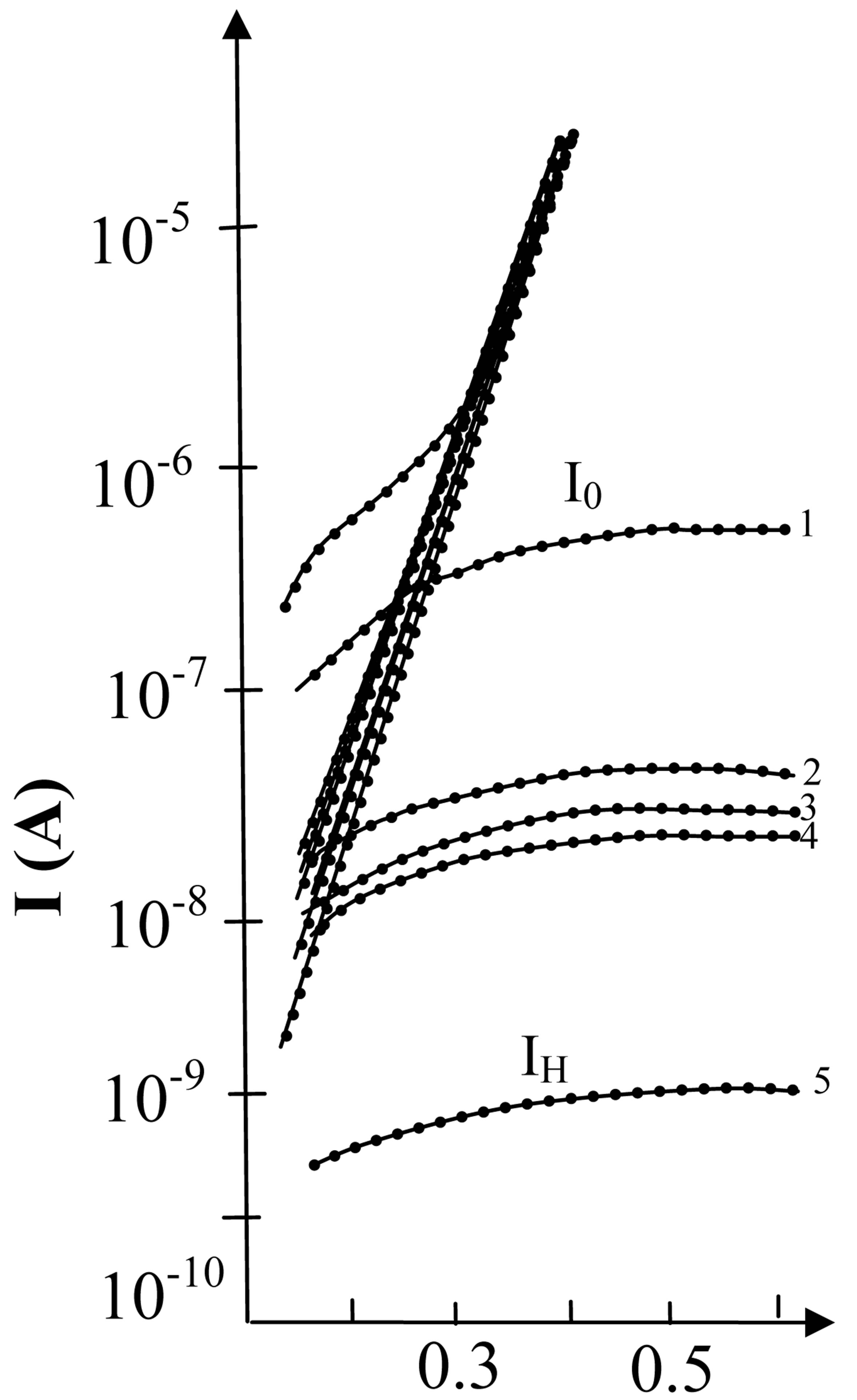
Figure 3. Current-voltage characteristic of αPbSb-nSi ShD in normal, artificial degraded and annealed conditions. IH-Normal (intact) diodes Shottki, Io-diodes directly after the influence of identer (t = 0), (V = 0.20 v)
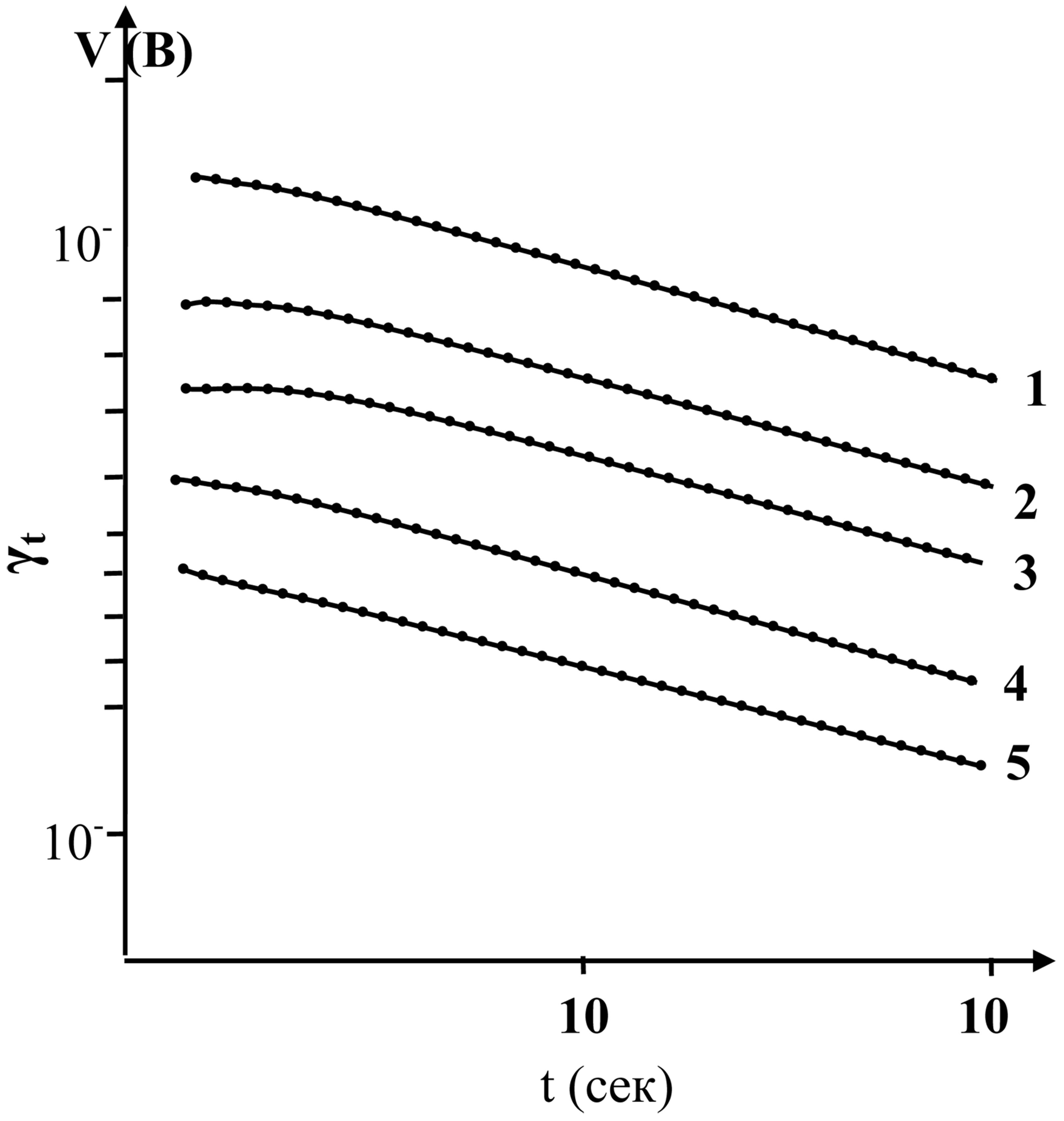
Figure 4. A relation of γt from annealing time at various values of temperature of annealing, 1—473 K; 2—498 K; 3—523 K; 4—548 K; 5—573 K.
from the above described experiments are presented: Is.c.- short circuits, Uх.х-open-circuit voltage, η-efficiency, Iret-a return current, А—dimensionless factor of the sample. In the table are represented values of these parameters after each stage of ultrasonic processing of the sample. Such built of the table allows to track on what value photo-electric parametres will change with supply on the sample of an ultrasonic wave with stringently set power, frequency and during set time. In investigated silicon SE, there is effective absorption of UIT in the places containing imperfections of a crystal lattice. The last represent dot defects and their complexes, and also claster formations and dispositions. As a result, there is a process of reorganisation of dot defects and their complexes possible.
4. Conclusions
Thus, it is possible to conclude that the superfluous current passes through mechanically dislocated areas of contact piece, and the reason of its occurrence is connected with violation of BS. It once again proves that occurrence of a superfluous current for αPbSb-nSi ShD near temperature of crystallization of an amorphous metal alloy is connected with the change of structure of an amorphous film of metal at transition into a polycrystalline state. From the received results it is obvious that change of parameters of annealing occurs for short initial periods, and the milestone of the process of annealing “cures” the damaged diodes. Certain level of annealing is reached at various parameters of annealing, annealing level of γt = 0.1 at Tann = 473 K is reached during t = 200 second, and at Tann = 523 K during t = 9 second
The results of conducted experiments show that UIT influences the character and degree of changes of the photoelectric and electrophysical properties of SE.
REFERENCES
- K. Mammadov, “Contact Piece Metal-Semiconductor with an Electrical Field of Stains,” Baku State University, Baku, 2004.
- SH. G. Askerov, SH. G. Aslanov and I. G. Pashayev, “Electrophysical Properties of Barrier Structures on the Basis of Silicon with an Amorphous Metal Alloy AluminiumNickel,” The Electronic Engineering, Microelectronic Devices, Vol. 6, No. 78. 1989, p. 46.
- N. A. Torhov, “Nature of Direct and Return Currents of Saturation in Contact Pieces Metal-Semiconductor with a Barrier of Shottki,” Semiconductors, Vol. 44, No. 6, 2010, p. 767
- SH. G. Askerov, “Influence of Degree of Non-Uniformity of Border of Section on Electrophysical Properties of Structures Metal-Vacuum and Metal-Semiconductor,” the Thesis for a Doctor’s, Baku State University, Baku, 1992. p. 399.
- N. A. Gusejnov, S. G. Askerov, J. M. Olih, et al., “Processing of the Irradiated Solar Cells by Means of Ultrasound,” Geliotehnika, No. 2, 2006, p.17.
- A. N. Gontaruk, D. V. Korbutjak and E. V. Korbut, “Degrade-Relaxation Phenomena in Light Emitting p-n Structures on the Basis of Photodiode Gallium, Stimulated by Ultrasound,” Letters in JTF, Vol. 24, No. 15, 1998, p. 64.
- K. Suzuki, K. Hasimoto and Х. Fudzimori, “Amorphous Metals,” М: Metallurgy, 1987.
- I. B. Ermolovich and V. V. Milenin, “Konakovo of River В, et al., “Influence of Ultrasonic Processing on Microprocesses of Formation of Barriers of Shottki of Heterosystems M − n − n + GaAs (M=Pt, Cr, W),” Technical Physics Letters, Vol. 22, No. 6. 1996, p. 33.
- G. D. Melebaeva, Д. Melebaev, J. V. Rud and V. J. Rud “Photosensitivity of Barriers of SHOTTKI Ni-GaAs,” Semiconductors, Vol. 43, No. 1, 2009, p. 34
- I. V. Ostrovskij, L. P.Steblenko and A. B. Nadtochy, “Formation of the Superficial Hardened Layer in Nondislocated Silicon at Ultrasonic Processing,” Semiconductors, Vol. 34, No. 3. 2000, p. 257.
- The Parchinsky Item B., S. I. Vlasov and L. G. Ligaj, “Probe of Influence of Ultrasonic Effect on Generating Characteristics of Previously Irradiated Border of Silicon —Dioxide Silicon,” Semiconductors, Vol. 40, No. 7, 2006, pp. 829- 832.
- The Parchinsky Item B., S. I. Vlasov, R. A. Muminov, et at., “Influence of Ultrasound on Parameters of Structures of Metal-Dielectric-Semiconductor,” Letters in JTF, Vol. 26, No. 10. 2000, p. 40.