Optics and Photonics Journal
Vol. 3 No. 5 (2013) , Article ID: 36243 , 7 pages DOI:10.4236/opj.2013.35048
FDTD Simulation of Three Photon Absorption and Realization of NAND Gate with GaAs Wire Waveguide
1Department of Physics, Kanksa Academy of Technology & Management, Burdwan, India
2Department of Electronics & Communication Engineering, Banwarilal Bhalotia College, Asansol, India
Email: research_phy@rediffmail.com, dkbbcasn@gmail.com
Copyright © 2013 Ivy Dutta et al. This is an open access article distributed under the Creative Commons Attribution License, which permits unrestricted use, distribution, and reproduction in any medium, provided the original work is properly cited.
Received June 5, 2013; revised July 10, 2013; accepted August 1, 2013
Keywords: Three Photon Absorption; Fifth Order Nonlinearity; FDTD; Full Vector Finite Difference Method; Pump Beam and Probe Beam
ABSTRACT
GaAs has high three photon absorption (3PA) co-efficient at mid-infrared wavelength like 2.2 mm and waveguides can be formed with this material like silicon nano-wires. It is shown that three-photon-absorption in GaAs wire waveguide can be utilized to form NAND gate. Three-photon-absorption is incorporated in one-dimensional Finite Difference Time Domain (FDTD) equations. The evolution of a probe pulse under the influence of a pump pulse through crossabsorption in a waveguide is investigated using FDTD simulation, where the dominant process is nonlinear three-photon-absorption. Output probe power dependence on input pump power shows that GaAs waveguide NAND gate has higher extinction ratio in comparison to NAND gate using two-photon-absorption in silicon waveguide.
1. Introduction
GaAs is an important material in the realm of nonlinear photonics. GaAs/AlGaAS multiple quantum well structures (MQW) exhibit high Kerr-type nonlinearity due to exitonic resonances near the band gap [1]. In a directional coupler with nonlinear core or cladding region, power exchanges between the guides ceases when the input power is raised beyond a critical power [2-6]. This fact was used to design and implement power switching at relatively low powers using such MQW structures although large loss in the medium near the bandgap is an impediment [7,8].
On the other hand, composites of GaAs, like AlGaAS, InGaAs can be used to form semiconductor optical amplifiers (SOA). SOAs are low-cost optical amplifiers—a potential candidate to replace electronic devices in local distribution systems for faster applications. Many signal processing elements and logic gates [9-12] have been proposed and verified. However, the speed of these devices is also limited by the response time of the carriers.
After some pioneering works by M. Lipson et al., silicon photonics [13] is a very active field of study for the realization of all optical logic gates. Kerr nonlinearity of silicon is not very high—it is about 10−9 times than GaAs MQW structure. Integrated photonic circuits were formed with micro-ring resonators using free carrier dispersion [14] and with slot waveguides using field switching in the middle cladding region [15]. Other nonlinear effects of silicon like Two Photon Absorption [16,17], Raman Effect [18,19], Polarization Rotation [20], Fourwave Mixing [21,22] can also be used to realize all optical logic gates.
One of the major advantages of silicon is that waveguides can be formed with very small transverse dimensions—in the range of few nm, which are called silicon wires. GaAs is also compatible with silicon platform and GaAs wires can be formed with appreciable bending [23]. Other nonlinear effects of GaAs are also prominent and still not fully explored [24].
It is observed that silicon photonics can be used with higher efficiency in the mid infra-red region i.e. 2 - 10 mm [25]. GaAs has some superior characteristics in this wavelength range and one can tap amplification also due to direct bandgap nature of this material [26].
T. K. Liang et al. [16] proposed ultrafast all optical NOR gates based on two photon absorption (2PA) in silicon. We have earlier shown that NAND gates can also be formed, in principle, using 2PA in silicon, but the extinction ratio is poor [27].
Between NOR and NAND gates based on absorption or loss, NAND gate is preferable because it has only one low output state. In this paper, we show that using 3PA in GaAs, NAND gates can be formed with better extinction ratio. Silicon has low 3PA coefficient, so it can not be used that way.
In Section 2, we have incorporated 3PA loss in the Ampere’s law of Maxwell’s equations. The inclusion of this nonlinear term makes FDTD update equations [28-30] complicated. We show a procedure to simplify the FDTD update equations. FDTD update equations are set up with 3PA process included and for simultaneous evolution of pump and probe pulses through cross-absorption. In Section 3, we first determined the effective index and modal field of the GaAs wire waveguide using our indigenously-developed full vector finite difference method without and with Kerr nonlinearity which leads to simplification of the FDTD formulation to one-dimension. We also discussed the effects of Kerr nonlinearity on the temporal evolution of the pump pulse. Then we validated our FDTD equations reproducing the theoretical law of power attenuation during propagation along the waveguide. Next we determined the probe power output for various input pump powers for a fixed length of the waveguide. These studies form the basic of the NAND gate we design. The waveguide structure for this gate device and its working is also illustrated in this section.
2. Theory
The evolution of a single pump beam of intensity Ip in a medium with three-photon-absorption coefficient  is given by
 (1)
(1)
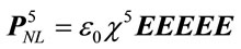
This can also be expressed in terms of the electric field  as
as
 (2)
(2)
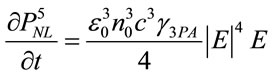
where  is the electric permittivity of free space, c the velocity of light in free space and
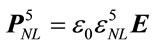
  is the effective index of the waveguide. The above process involves a fifth order nonlinear interaction. The polarization related to this process
 (3)
(3)
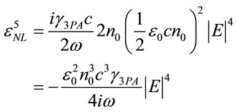
The imaginary part of  contributes to 3PA process. One can write
 (4)
(4)
where  is the relative electric permittivity arising from fifth order nonlinearity. Then considering only 3PA process
 (5)
(5)
So,
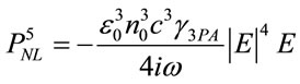 (6)
(6)
Multiplying both sides of (6) by  and replacing it by
 (7)
(7)
Maxwell’s equation (Ampere’s law) with linear and nonlinear polarization can be expressed as
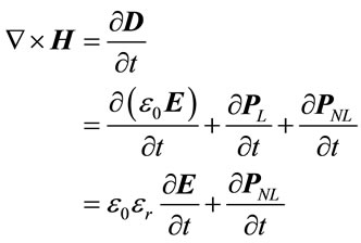 (8)
(8)
where  is the linear part of relative electric permittivity.
We consider only 3PA effect in the nonlinear polarization. Then putting (7) in (8)
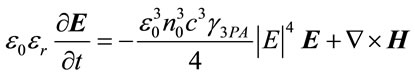 (9)
(9)
In our 1D FDTD, we take , the effective index of the waveguide. Then writing
 , (9) takes the form
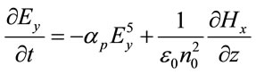
This leads to the following finite difference equation for electric field update
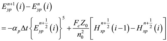 (10)
(10)
where  is the Courant number. It is taken as unity. Z0 is the impedance of the vacuum.
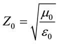
The other FDTD equation for magnetic field update keeps its usual form
 (11)
(11)
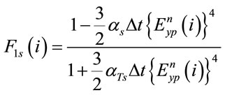
To simplify FDTD update Equation (10), one can make use of Taylor series expansion [31]
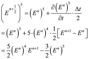
Then Equation (10) takes the form
 (12)
(12)
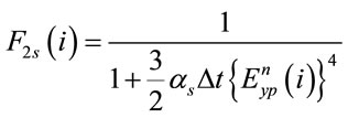
where
 (13a)
(13a)
 (13b)
(13b)
When one pump beam and a probe beam of different frequencies are present, the change in intensity of the pump and probe beam can be obtained using (3),
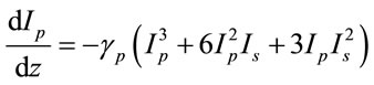 (14a)
(14a)
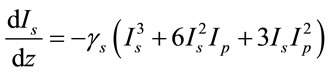 (14b)
(14b)
 are the 3PA coefficients of pump and probe waves respectively. The probe beam is much weaker than the pump beam. Keeping the dominant terms in (13),
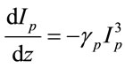 (15a)
(15a)
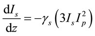 (15b)
(15b)
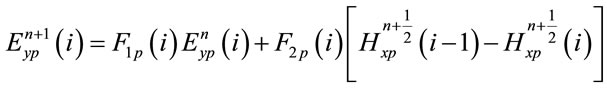
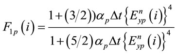
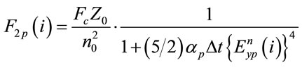
The update equation for the pump and probe electric fields has the same form as (12). Denoting the probe fields by  and
and , in the update Equation (12), using (15b) the coefficients
  and
and  are given by
 (16a)
(16a)
 (16b)
(16b)
3. Results and Discussions
The structure of the GaAs wire [23] is shown in Figure 1. The GaAs wire waveguide having a square cross-sectional area of width W rests on a thick SiO2 platform. The wavelength of the probe beam is taken to be 2.2 mm; the waveguide is single-moded at this wavelength. We have used Gaussian pulses of 0.5 ps width for the pump beam and continuous oscillatory field of wavelength 2.2 µm for the probe beam.
The peak strength of the probe beam is taken to be 10−2 times the pump strength. The centre wavelength of the pump beam is set at slightly different value to filter out the pump wave at the output where the probe is also present. The choice of the pump wavelength and width W of the waveguide depends on several factors which is discussed in the following.
The gates, we propose, works on the attenuation of optical power due to 3PA as it propagates along the waveguide. There is also another third order nonlinear process in this level—Kerr effect. This process changes the shape of the transverse modal field distribution and also the pulse shape in the time domain. So, it is important to look at the role of this effect while the power in the waveguide changes during propagation.
To estimate the effect of Kerr nonlinearity in the modal field distribution, we made a full vector finite difference method (FVFDM) modal analysis of the waveguide taking Kerr effect into account. The FVFDM we have developed on our own and coded in Matlab. It is very fast, works on the inverse iteration method [32]. We found the effective area Aeff of the waveguide given by [33]
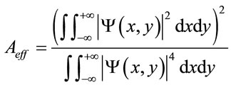 (17)
(17)
 is the transverse field distribution, either Efield or H-field.
Nonlinearity is incorporated in this scheme through the modification in the refractive index profile and iteration [6]. The difference of effective index values and modal field distributions of the waveguide, with and without nonlinearity at the maximum power –2 GW/cm2 we consider, is quite small; the change in the effective area is only 0.5%. So one can neglect the transverse distribution of the modal field and use one-dimensional FDTD to extract the power evolution along the waveguide. The refractive index of GaAs at 2.2 mm wavelength is 3.3552 and that of SiO2 is 1.4350. Then effective index of the wire waveguide n0 = 1.542 and the effective area is 0.23 µm2.
When one uses ultra-short pulses and high power to tap nonlinear absorption like 2PA or 3PA, dispersion and
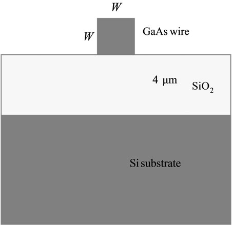
Figure 1. Schematic diagram of GaAs wire.
self-phase-modulation (SPM) effects must be investigated.
We have found group velocity dispersion (GVD) parameter b2 and third order dispersion (TOD) parameter b3 with our FVFDM for a range of wavelengths. Material dispersion and waveguide dispersion both are considered simultaneously in the analysis. Variation of b2 with l within the range of our interest (1.8 to 2.1 µm), is shown in Figure 2 for three widths of the GaAs wire. Variation of b3 is shown in Figure 3.
It is observed that for 440 µm2 cross-section, b2 is almost flat but the value is near −10 ps2/m. For ultra-short pulses, GVD must be very low to avoid pulse dispersion [33].
To set b2 at a low value near l = 2 µm, 420 µm2 is most suitable. Near zero dispersion wavelength, one must take care of Third Order Dispersion (TOD) or b3. Figure 3 shows b3 is low for 420 m2 cross-section near l = 2 µm.
At 2.02 µm wavelength, length associated with GVD,  , length associated with TOD,
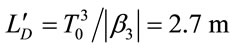 .
.
At 2 µm, 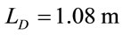 and
and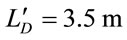 .
.
So, around 2 µm wavelength, dispersion wavelengths  and
and  can be set to values large compared to the desired length of the waveguide, 0.5 cm.
Nonlinear Kerr coefficient of GaAs, 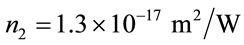 [34], is about thousand times higher compared to that in silica. So, it may give rise to appreciable SPM effects. SPM is appreciable in a waveguide when the length of propagation L is comparable to the nonlinear length
  defined by [33]
where  and
and  is the peak power of the pulse.
 is determined with FVFDM; at l = 2 µm, it is
Figure 2. Variation of GVD (b2) with l.
Figure 3. Variation of TOD (b3) with l.
0.23 µm2. Maximum intensity of the pump pulse used here is around 2 GW/cm2. This gives  Watt and
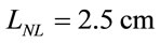 . Since peak power falls due to 3PA during propagation,
  can be considered large compared to the waveguide length 0.5 cm; therefore SPM effects can be neglected. The value of
  is 0.32 cm3/GW2 [34], at the probe wavelength 2.2 µm. At the wavelength of the pump beam – 2 mm,
  is 0.18 cm3/GW2.
The NAND gate device that acts on the principle of three-photon cross absorption is shown in Figure 4. Two pump beams are fed into the waveguide through S-bends and the probe beam is injected straight at the center. At first, we have validated our FDTD formulas (11), (12) with co-efficients given by (13) and (16). Figure 5 shows the attenuation of the pump and probe beams during propagation through a distance of 1 cm, as obtained with FDTD simulation and from the theoretical result— Equation (15). Pump and probe intensity variation obtained from FDTD simulation is shown with red line
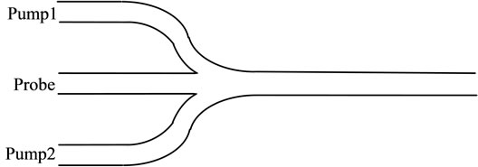
Figure 4. Structure of the NAND gate device.
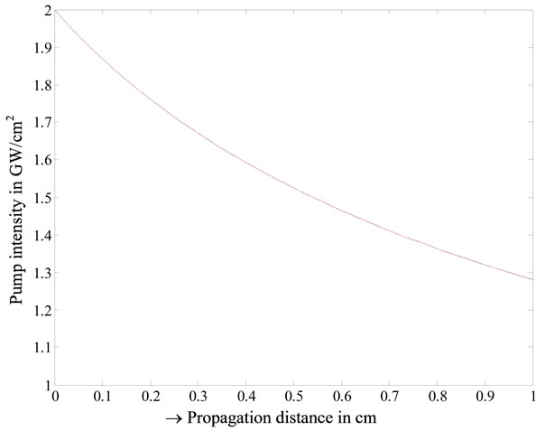
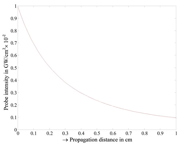
Figure 5. Attenuation of pump and probe intensity with propagation. Black line—FDTD; Red line—Equation (15).
curve and that from Equation (15) is shown with black line curve. The curves are almost coincident.
We have coded our FDTD program in MATLAB. The probe beam develops an inverted Gaussian pulse at the point of the pump beam. We have set up a program to get the envelope of the probe beam which shows the form of the dark pulse clearly. We have taken Δz = 4.28 × 10⁻⁸ μm; it is observed that such a fine numerical grid is necessary for proper development of the probe pulse. We have taken numerical window size = 10,000 × Δz and PML layers of 10 cell width. After 15,420 time steps, as the fields reach the right edge, they are partially shifted to the left and the probe field is fed into the input at the right phase. In this way, same numerical window can be used taking time update as long as one wants saving computational time enormously.
The evolution of the pump pulse and dark probe pulse are shown in Figure 6. One pump pulse and its corresponding probe pulse are shown near the input end; the shape of those pulses is also shown at the output end— after propagation through 1 cm length of the waveguide.
The minimum of the dark pulse after 0.5 cm propagation for a range of input pump intensity from 0 to 2 GW/cm2, is shown in Figure 7. It shows that for 0.9 GW/cm2 pump input intensity, the output probe intensity is down by about 70% and when the input intensity is 1.8 GW/cm2, the output is down by about 36%. If 50% intensity level is used as threshold, the switching of the output from high to low as the input intensity is changed from 0.9 to 1.8 GW/cm2 can be used to form a NAND gate with the gate structure of Figure 4 as shown in Table 1.
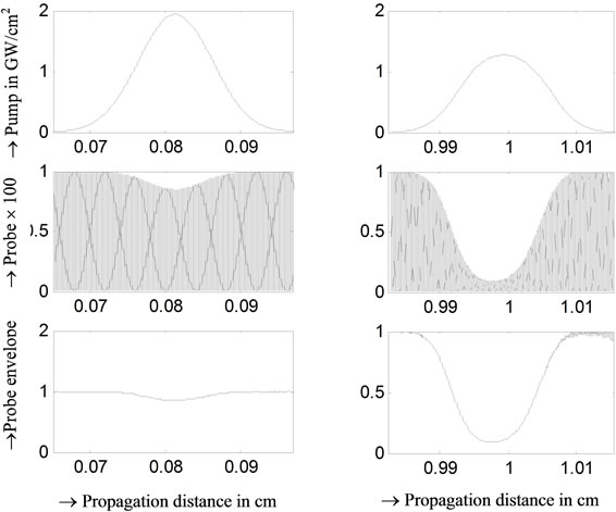
Figure 6. Pump pulse and dark pulse formation in the probe beam.
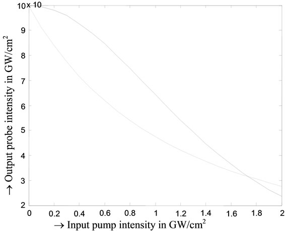
Figure 7. Variation of probe intensity with pump intensity for 0.5 cm guide length.
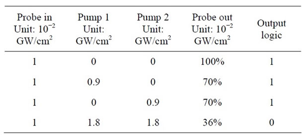
Table 1. Realization of NAND gate.
In Figure 7, the dotted line is the corresponding probe intensity variation in silicon wire waveguide based on two photon absorption (wavelength 1.55 mm, β2PA = 0.9 cm/GW).
The curve for Si-wire waveguide in Figure 7 shows that NAND switching can be obtained for 0.5 cm guide length. Without any pump input, probe intensity gets out undiminished. When pump 1 or pump 2 is present and equal to 0.9 GW/cm2, the probe output is 51%. When both pump 1 and pump 2 are present, the output is attenuated down to 34%. If 40% probe power is taken as threshold, the output is low only when both pump 1 and pump 2 are present; NAND switching can be realized with the Si-wire waveguide structure shown in Figure 4. However, GaAs waveguide has higher extinction ratio and higher difference between high and low states.
4. Conclusion
GaAs has some superior nonlinear behavior than silicon and its potentiality is not yet fully explored. We have considered a GaAs wire waveguide and determined its effective index with a full vector finite difference method with and without Kerr nonlinearity. The small difference of the effective index values when Kerr nonlinearity is taken into account prompted us to simulate the evolution of pump and probe field along the same waveguide through cross-absorption using one-dimensional FDTD. In this paper, we have incorporated three-photon-absorption in one-dimensional FDTD update equations. GaAs has significant three-photon-absorption co-efficient. We have considered a GaAs wire waveguide structure (Figure 4) that takes in two pump beams and one probe beam, puts them into a single waveguide. We have shown that one can realize NAND gate with this structure where the intensity of the input pump beams are the input states and the output probe intensity is the output state. Similar gate structure can be formed if GaAs is replaced with Si-wire waveguide but that has lower extinction ratio.
REFERENCES
- D. A. B. Miller, D. S. Chemia, D. J. Eilenberger, P. W. Smith, A. C. Gossard and W. T. Tsang, “Large Room Temperature Optical Nonlinearity in GaAs/Ga1-xAlxAs Multiple Quantum Structures,” Applied Physics Letters Vol. 41, No. 8, 1982, pp. 679-681. doi:10.1063/1.93648
- S. M. Jensen, “The Nonlinear Coherent Coupler,” IEEE Journal of Quantum Electronics, Vol. 18, No. 10, 1982, pp. 1580-1583. doi:10.1109/JQE.1982.1071438
- X. J. Meng and N. Okamoto, “Improved Coupled Mode Theory for Nonlinear Directional Couplers,” IEEE Journal of Quantum Electronics, Vol. 27, No. 5, 1991, pp. 1175-1181. doi:10.1109/3.83374
- I. M. Uzonov, R. Muschall, M. Golles, Y. S. Kivahar, B. A. Malomed and F. Lederer, “Pulse Switching in Nonlinear Fiber Directional Couplers,” Physical Review E, Vol. 51, No. 3, 1995, pp. 2527-2537. doi:10.1103/PhysRevE.51.2527
- K. G. Kalonakis and E. Palspalkis, “Optical Switching in a Symmetric Three-Waveguide Nonlinear Directional Coupler,” Journal of Modern Optics, Vol. 52, No. 13, 2005, pp. 1885-1892. doi:10.1080/09500340500141755
- D. Kumbhakar, “Nonlinear Coherent Directional Coupler: Coupled Mode Theory and BPM Simulation,” International Journal of Optics, Vol. 2012, 2012, Article ID: 173250.
- S. Trillo and S. Wabnitz, “Nonlinear Dynamics and Instabilities of Coupled Waves and Solitons in Optical Fibers,” In: C. G. Someda and G. Stegeman, Eds., Anisotropic and Nonlinear Optical Waveguides, Elsevier, Amsterdam, 1992.
- P. R. Berger, P. K. Bhattacharya and S. Gupta, “A Waveguide Directional Coupler with a Nonlinear Coupling Medium,” IEEE Journal of Quantum Electronics, Vol. 27, No. 3, 1991, pp. 788-795. doi:10.1109/3.81390
- M. J. Connelly, “Semiconductor Optical Amplifiers,” Kluwer Academic Press, Dordrecht, 2002.
- K. E. Stubkjar, “Semiconductor Optical Amplifier-Based All-Optical Gates for High Speed Processing,” IEEE Journal on Selected Topics on Quantum Electronics, Vol. 6, No. 6, 2000, pp. 1428-1435. doi:10.1109/2944.902198
- K. Shimomura and S. Arai, “Semiconductor Waveguide Optical Switches and Modulators,” Fiber and Integrated Optics, Vol. 13, No. 1, 1994, pp. 65-100. doi:10.1080/01468039408202222
- M. F. S. Ferreira, “Optical Amplifiers,” In: R. G. Driggers, Ed., Encylopedia of Optical Engineering, Taylor & Francis, London, 2011.
- Q. Lin, O. J. Painter and G. P. Agrawal, “Nonlinear Optical Phenomena in Silicon Waveguides: Modeling and Applications,” Optics Express, Vol. 15, No. 25, 2007, pp. 16604-16644. doi:10.1364/OE.15.016604
- Q. Xu and M. Lipson, “All-Optical Logic Based on Silicon Micro-Ring Resonators,” Optics Express, Vol. 15, No. 3, 2007, pp. 924-929. doi:10.1364/OE.15.000924
- Q. Xu, V. R. Almeida, R. R. Panepucci and M. Lipson, “Experimental Demonstration of Guiding and Confining Light in Nanometer-Size Low Refractive-Index Material,” Optics Letters, Vol. 29, No. 14, 2004, pp. 1626- 1628. doi:10.1364/OL.29.001626
- T. K. Liang, L. R. Nunes, M. Tsuchiya, K. S. Abedin, T. Miyazaki, D. Van Thourhout, W. Bogaerts, P. Dumon, R. Baets and H. K. Tsang, “High Speed Logic Gate Using Two-Photon Absorption in Silicon Waveguides,” Optics Communications, Vol. 265, No. 1, 2006, pp. 171-174. doi:10.1016/j.optcom.2006.03.031
- K. Mukherjee and D. Kumbhakar, “Simulation and Method Of Implementation of All Optical Logic Gates Based on Two Photon Absorption in Silicon Wire Wave Guide,” Optik, Vol. 123, No. 6, 2011, pp. 489-493. doi:10.1016/j.ijleo.2011.05.012
- V. M. N. Passaro and F. De Leonards, “All Optical AND Gate Based on Raman Effect in Silicon-On-Insulator Waveguide,” Optical and Quantum Electronics, Vol. 38, No. 9-11, 2006, pp. 877-888. doi:10.1007/s11082-006-9021-0
- D. Dimitropoulos, R. Claps, Y. Han and B. Jalali, “Nonlinear Optics in Silicon Waveguides: Stimulated Raman Scattering and Two-Photon Absorption,” Proceedings of SPIE Vol. 4987, Integrated Optics: Devices, Materials, and Technologies VII, San Jose, 2003, pp. 140-148.
- J. Y. Lee, L. Yin, G. P. Agrawal and P. M. Fauchet, “Ultrafast Optical Switching Based on Nonlinear Polarization Rotation in Silicon Waveguides,” Optics Express, Vol. 18, No. 11, 2010, pp. 11514-11523. doi:10.1364/OE.18.011514
- F. D. Leonardis and V. M. N. Passaro, “Efficient Wavelength Conversion in Optimized SOI Waveguides via Pulsed Four-Wave Mixing,” Journal of Lightwave Technology, Vol. 29, No. 23, 2011, pp. 3523-3535. doi:10.1109/JLT.2011.2169937
- S. M. Gao, Z. Q. Li and X. Z. Zang, “Power-Attenuated Optimization for Four-Wave Mixing-Based Wavelength Conversion in Silicon Nanowire Waveguides,” Journal of Electromagnetic waves and Applications, Vol. 24, No. 8-9, 2010, pp. 1255-1265. doi:10.1163/156939310791586142
- R. Katouf, N. Yamamoto, A. Kanno, N. Sekine, K. Akahane, H. Sotobayashi1, T. Isu and M. Tsuchiya, “Ultrahigh Relative Refractive Index Contrast GaAs Nanowire Waveguides,” Applied Physics Express, Vol. 1, No. 12, 2008, pp. 122101-122103. doi:10.1143/APEX.1.122101
- A. Hartsuiker, P. J. Harding, Y. R. Nowicki-Bringuier, J. M. Gérard and W. L. Vos, “Kerr and Free Carrier Ultrafast All-Optical Switching of GaAs/AlAs Nanostructures near the Three-Photon Edge of GaAs,” Journal of Applied Physics, Vol. 104, No. 8, 2008, Article ID: 083105. doi:10.1063/1.3000098
- G. Z. Mashanovich, M. M. Milosevic, M. N. Nedeljkovic, N. Owens, B. Xiong, E. J. Teo and Y. Hu, “Low Loss Silicon Waveguides for The Mid-Infrared,” Optic Express, Vol. 19, No. 8, 2011, pp. 7112-7119. doi:10.1364/OE.19.007112
- E. Guillotel, M. Ravaro, F. Ghiglieno, M. Savanier, I. Favero, S. Ducci and G. Leo, “GaAs/AlOx Nonlinear Waveguides for Infrared Tunable Generation,” In: K. Y. Kim, Ed., Advances in Optical and Photonic Devices, Chapter 8, Croatia, 2010, pp. 137-160. doi:10.5772/7144
- A. R. Chowdhury, I. Dutta, K. Mukherjee and D. Kumbhakar, “FDTD Simulation of Two Photon Absorption in Silicon Waveguide and Realization of All Optical Logic Gates,” Proceedings of Frontiers in Optics and Photonics, XXXVI OSI Symposium, Delhi, 3-5 December 2011, p. 245.
- A. Taflove and S. C. Hagness, “Computational Electrodynamics: The Finite Difference Time Domain Method,” 2nd Edition, Artech House, Norwood, 2000.
- C. M. Dissanayake, M Premaratne, I. D. Rukhlenko and G. P. Agrawal, “FDTD Modeling of Anisotropic Nonlinear Optical Phenomena in Silicon Waveguides,” Optic Express, Vol. 18, No. 20, 2010, pp. 21427-21448. doi:10.1364/OE.18.021427
- N. Suzuki, “FDTD Analysis of Two-Photon Absorption and Free-Carrier Absorption in Si High-Index-Contrast Waveguides,” Journal of Lightwave Technology, Vol. 25, No. 9, 2007, pp. 2495-2501. doi:10.1109/JLT.2007.903298
- E. P. Kosmidou and T. D. Tsiboukis, “An FDTD Analysis of Photonic Crystal Waveguides Comprising ThirdOrder Nonlinear Materials,” Optical and Quantum Electronics, Vol. 35, No. 10, 2003, pp. 931-946. doi:10.1023/A:1025122517879
- W. H. Press, S. A. Teukolsky, W. T. Vetterling and B. P. Flannery, “Numerical Recipe in Fortran 90,” Cambridge University Press, Cambridge, 2001.
- G. P. Agrawal, “Nonlinear Fiber Optics,” 3rd Edition, Academic Press, San Diego, 2001.
- W. C. Hurlbut, Y. S. Lee, K. L. Vodopyanov, P. S. Kuo and M. M. Fejer, “Multiphoton Absorption and Nonlinear Refraction of GaAs in the Mid-Infrared,” Optics Letters, Vol. 32, No. 6, 2007, pp. 668-670. doi:10.1364/OL.32.000668