Journal of Encapsulation and Adsorption Sciences
Vol.2 No.1(2012), Article ID:18303,4 pages DOI:10.4236/jeas.2012.21002
Effect of Pixellization on Efficiency and Stability of MEH-PPV Based Polymer Light-Emitting Diodes
1Department of Materials and Metallurgical Engineering, Indian Institute of Technology, Kanpur, India
2Samtel Centre for Display Technologies, Indian Institute of Technology, Kanpur, India
Email: *raviravi82@gmail.com
Received December 9, 2011; revised January 18, 2012; accepted February 20, 2012
Keywords: Organic light-emitting diodes; Pixellization; Isolation layer; Electroluminescence Quantum Efficiency
ABSTRACT
Organic light-emitting diodes are generally depicted as sequential deposition of active layers and electrodes onto a substrate, but commercial devices are fabricated using pixellization technique, where an insulator layer is introduced between the indium tin oxide and organic layer to define the area of the active device. Here, we have inserted a layer of photoresist (thickness ~ 200 nm) at the edge of patterned anode (indium tin oxide) and between the anode and hole transport layer (Poly 3, 4-ethylenedioxythiophene poly styrenesulfonate) to examine its effect on the leakage current of organic light-emitting diode and on the electron-hole recombination ratio in the emission area, as a result increasing the luminance efficiency. Current leakage causes the loss of charges, which adversely affects the recombination of electrons and holes in the emitting zone and results in poorer luminance efficiency. In this paper, we report the effect of pixellization on current density-voltage, luminescence-voltage and degradation behavior of single layer Poly[2-methoxy-5-(2’- ethylhexyloxy)-1, phenylene vinylene] based organic light-emitting diodes. Devices with isolation layer have 30% higher external electroluminescence quantum efficiency and reduced device degradation in comparison to without isolation layer.
1. Introduction
Application of organic light-emitting diodes (OLEDs) in flat-panel and flexible displays requires development of processing technology. There have been several papers reporting the optimization of hole injection, hole transporting, electron transporting and electron injection layers for a given emissive layer. The cathode of OLEDs is typically made of aluminum (Al) layer with Ca [1-4] or LiF [5-8] to boost the injection of electrons into the organic layer or a buffer layer is added to the anode [9], which also improves the device characteristics. Besides the multilayer active stack, the device structure can have the substantial effect on OLEDs characteristics and stability. Factors which contribute to degradation mechanisms for OLEDs are crystallization of the amorphous organics film [10], dark spot formation [11], quality of the polymer materials, and changes in morphology at the metal/organic interfaces [12,13].
In early models, the formation of dark spots was attributed to high local fields or high local Joule heating. High local fields in areas of electrode non-uniformity cause hot spots in OLEDs, and consequently result in pinholes in the top electrode, enhanced oxidation and ablation of the top electrode [14]. Also, high local Joule heating by high local currents causes interdiffusion at the hole transport layer/electron transport layer (HTL/ETL) interface and leads to a reduction of currents in the mixed area [15]. These have been identified as causes of device instability. The edges created due to Indium Tin Oxide (ITO) and cathode overlap can also affect the device stability because of high current density on the edges. Chung et al. [16] reported the result of insulation layer in OLED device. With the increase in the thickness of the Silicon Oxide (SiO2) the leakage current of the device reduces and which helps to improve the external electroluminescence quantum efficiency of the device.
In this study we insert, a layer of photo-resist, between the patterned ITO and cathode to explore its effect on the leakage current of OLEDs and on the electron-hole recombination in the emission area, and its effect on Luminance. The stability is also improved due to combined effect of reduced leakage and electric field at the edges of ITO by using isolation layer
2. Experimental
Devices were fabricated on 150 nm thick indium tin oxide (ITO) coated glass having a sheet resistance of 10 Ω/sq. The pattern of anode (ITO) was done on a glass substrate by photo-lithography. The ITO coated glass substrate was then ultrasonically cleaned using acetone, methanol and deionized (DI) water. After drying in vacuum (2 × 10⁻⁶ m bar) at 130˚C for 1hr, a layer of positive photo-resist as isolation layer was coated to define pixel using photo-lithography as shown in Figure 1(b). The pixel area is smaller than the anode areas to allow cov-
 (a)
(a)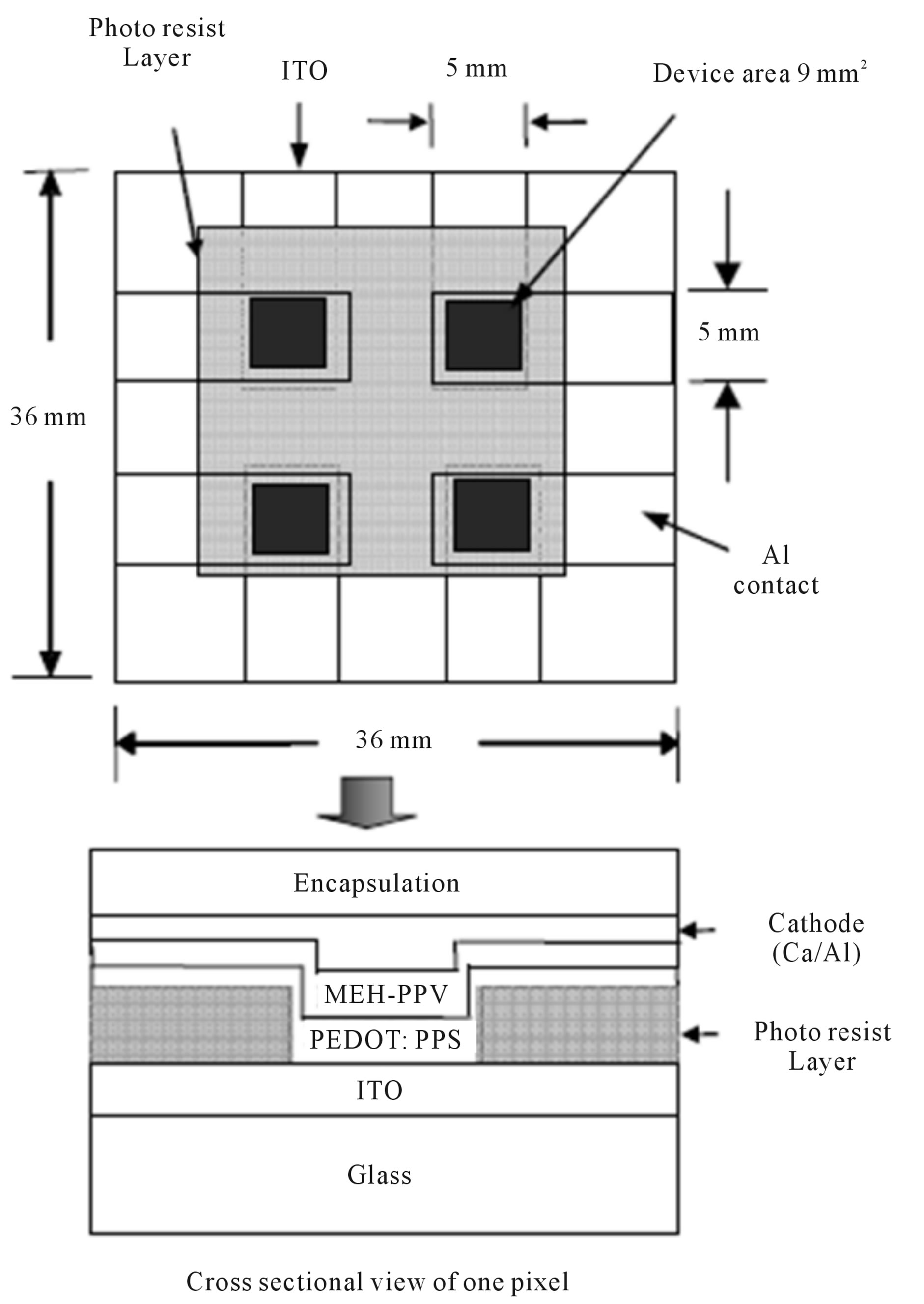 (b)
(b)
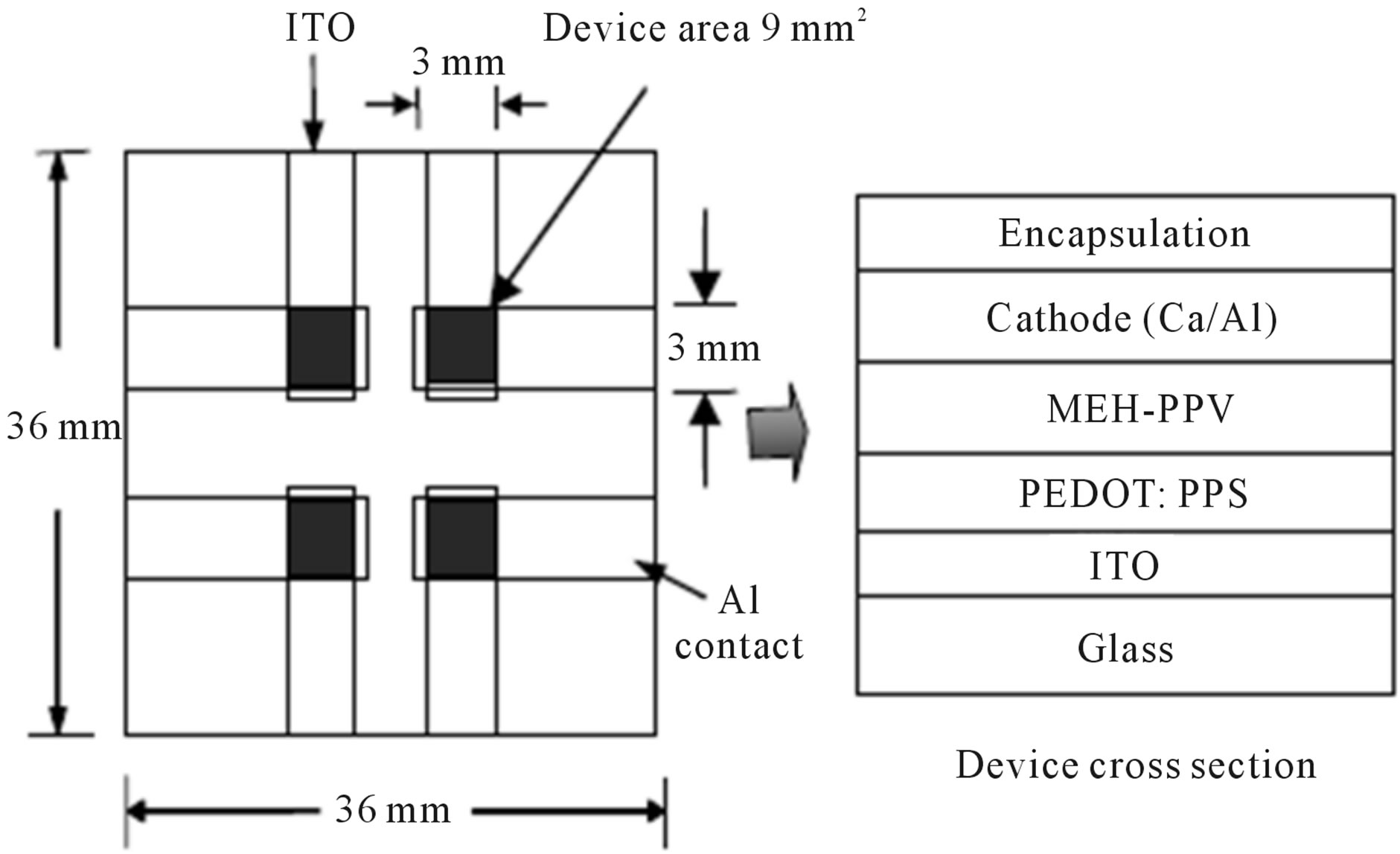
Figure 1. Pixel defined (a) without isolation layer & its cross-sectional view of devices (b) with the isolation layer (200 nm photo-resist).
erage of the edge of ITO pattern. The device without pixellization by isolation layer and its cross sectional view is shown in Figure 1(a). The emission area of both devices with and without the isolation area was fixed in the 9 mm2 rectangular form. The patterned substrate was then placed in ozone (350 sccm O2) for surface cleaning. PEDOT: PSS was spin coated over ITO to planarize surface spikes and increase the work function of the substrate. The PEDOT: PSS layer was then dried in vacuum (2 × 10⁻⁶ m bar) at 130˚C for 1 hr. Then MEHPPV solution in 50% xylene + 50% chloroform with 5mg/ml concentration was spin coated over PEDOT: PSS layer, which was subsequently dried in vacuum (2 × 10⁻⁶ m bar) at 120˚C for 1hr. Figure 2 shows the thickness of the polymer is optimize to achieve low turn-on voltage. The Ca/Al bilayer cathode was thermally evaporated in vacuum (3 × 10⁻⁶ m bar) onto the emitting layer. Finally the devices were encapsulated using a glass cover with UV cured epoxy to avoid penetration of oxygen and moisture. The final structure of the device was ITO (1400)/PEDOT: PSS (800)/MEH-PPV (1000)/Ca (300)/ Al (1000 in Å).
The luminance-current density-voltage (L-J-V) characteristics of the devices were measured after its fabrication. Minolta spectroradiometer (CS-1000) was employed to measure the luminance and spectrum, and Keithley- 6517 electrometer was employed as power supply and testing of current voltage characteristics. We have estimated the ELQE of the device, using a 6 inch integrating sphere (SPH-6-4 Sphere Optics Hoffman Engineering) and a calibrated silicon photodiode (S1226-8BQ TO-8 Hammamatsu) with spectral response range of 190 - 1100 nm wavelength. For degradation study, a constant voltage was applied, and the light output and current were monitored continuously.
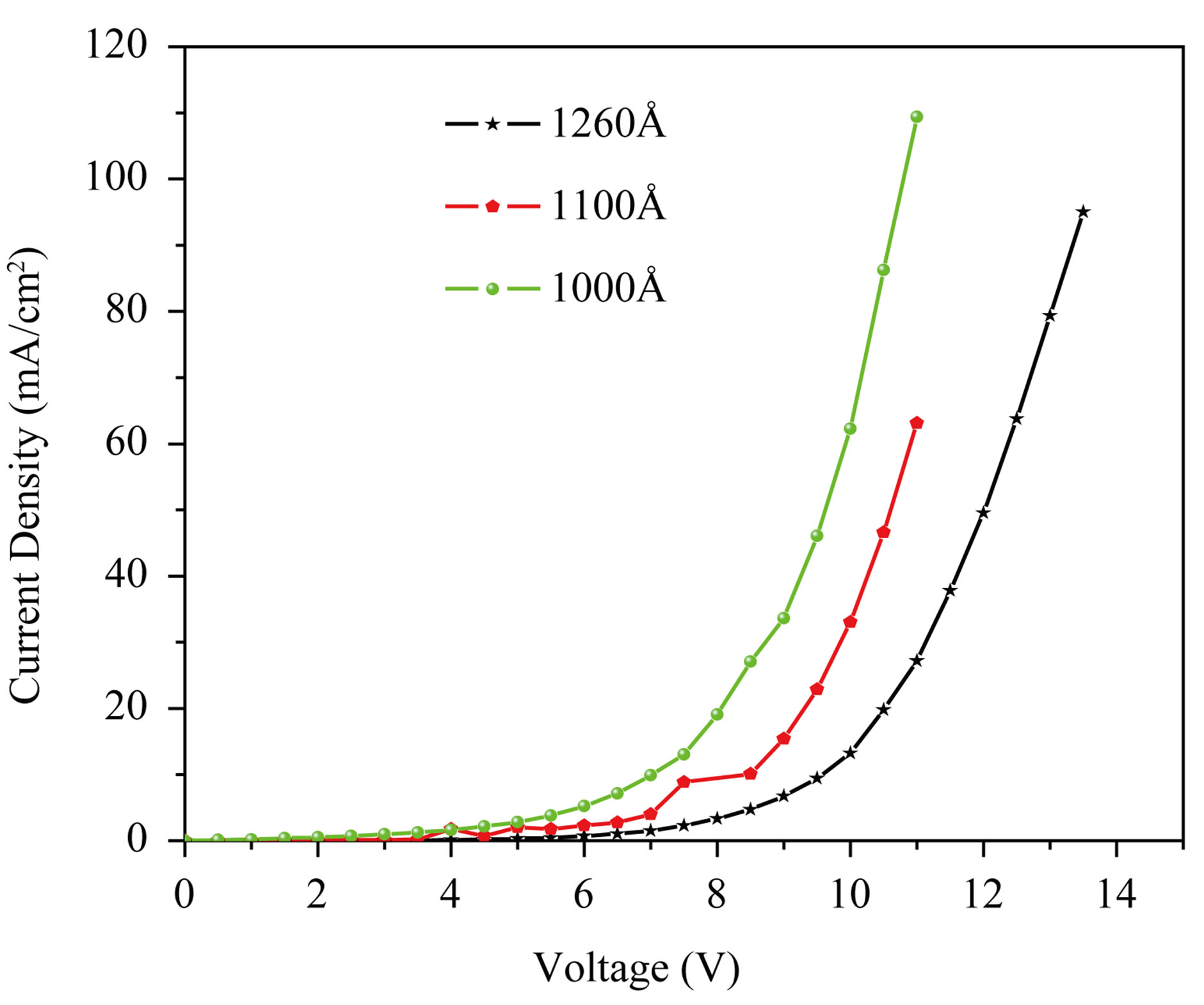
Figure 2. Current density—voltage characteristics of pixellized devices at different thickness of the polymer.
3. Results and Discussion
3.1. Electrical Characterization
Figures 3 and 4 shows the J-V and L-V characteristics of pixellized and unpixellized device respectively. As charges of the device without an isolation layer leak from the edge of emission area, electrons cannot effectively combine with holes in the emission area. It can be seen that on pixellization less current flows through the device and as a result luminescence is higher. And also at the same current density pixellized devices have the high luminescence (163 Cd/m2 for unpixcellized and 210 Cd/m2 for pixellized at 10 mA/cm2). This can be attributed to the fact that on pixellization the leakage current in the device is reduced as compared to the unpixellized devices. As a result number of electron-hole following through the emissive area of the device increases and hence the
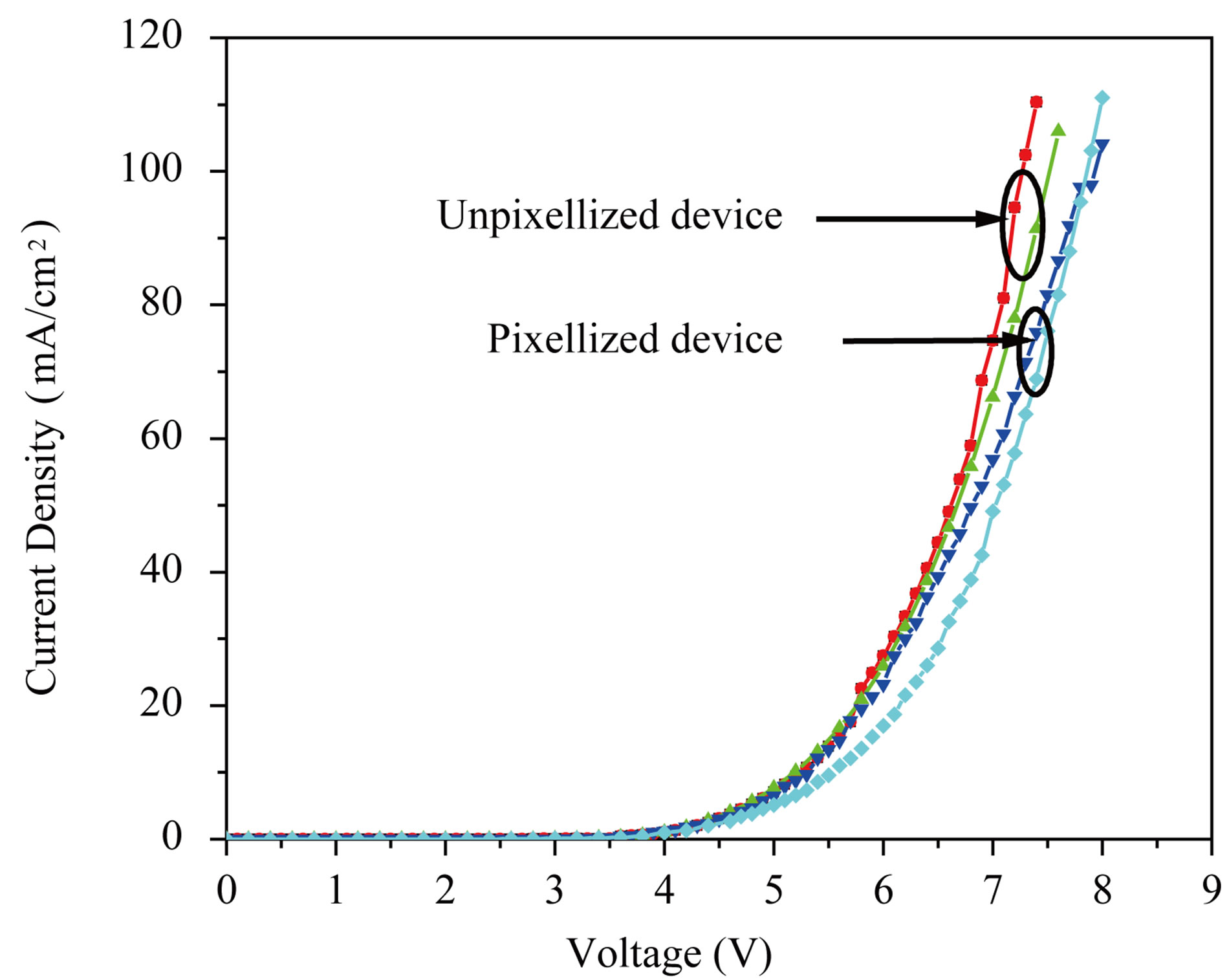
Figure 3. Current density—voltage characteristics for the pixellized and unpixellized devices.
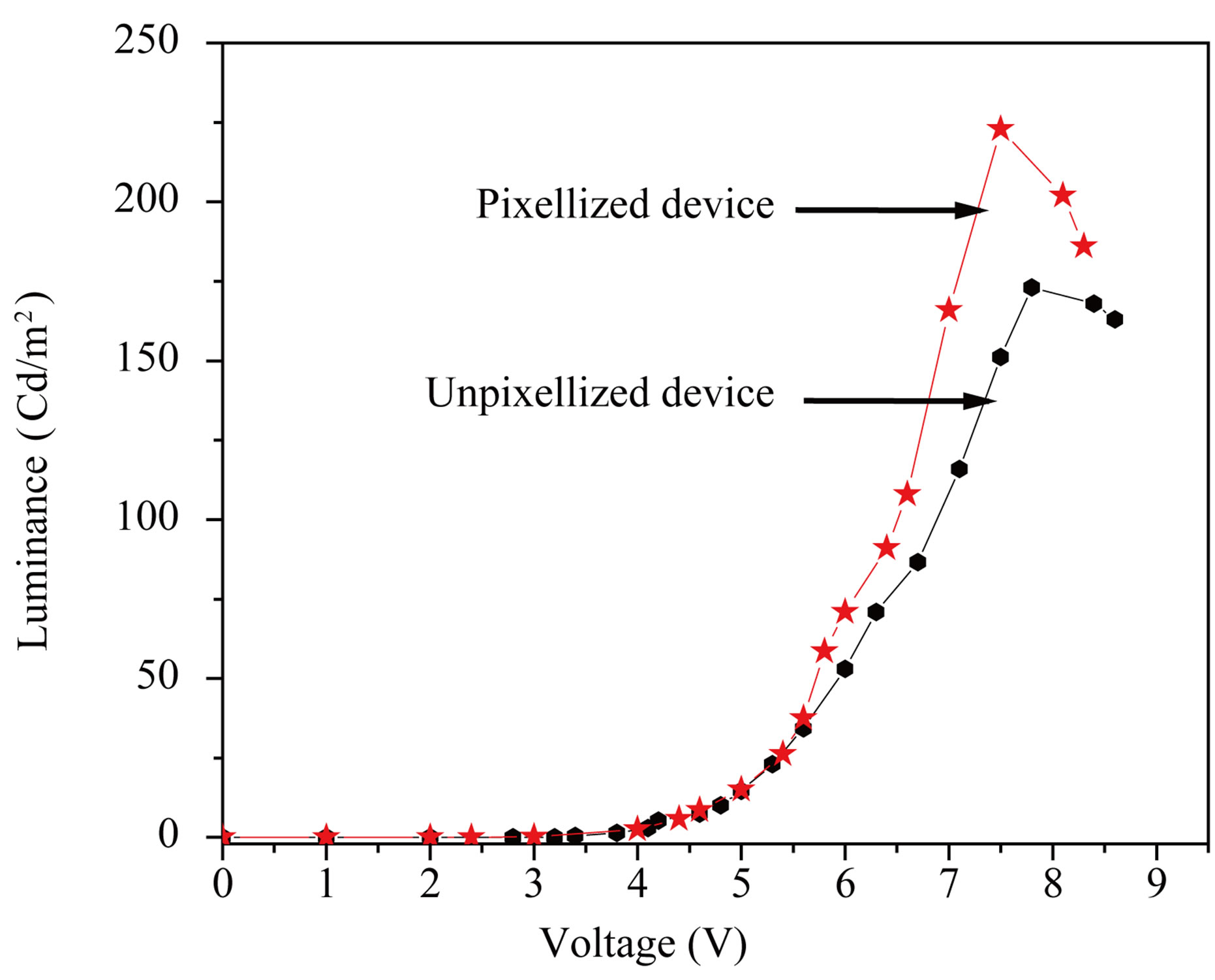
Figure 4. Luminance—Voltage (L-V) characteristics for the pixellized and unpixellized devices.
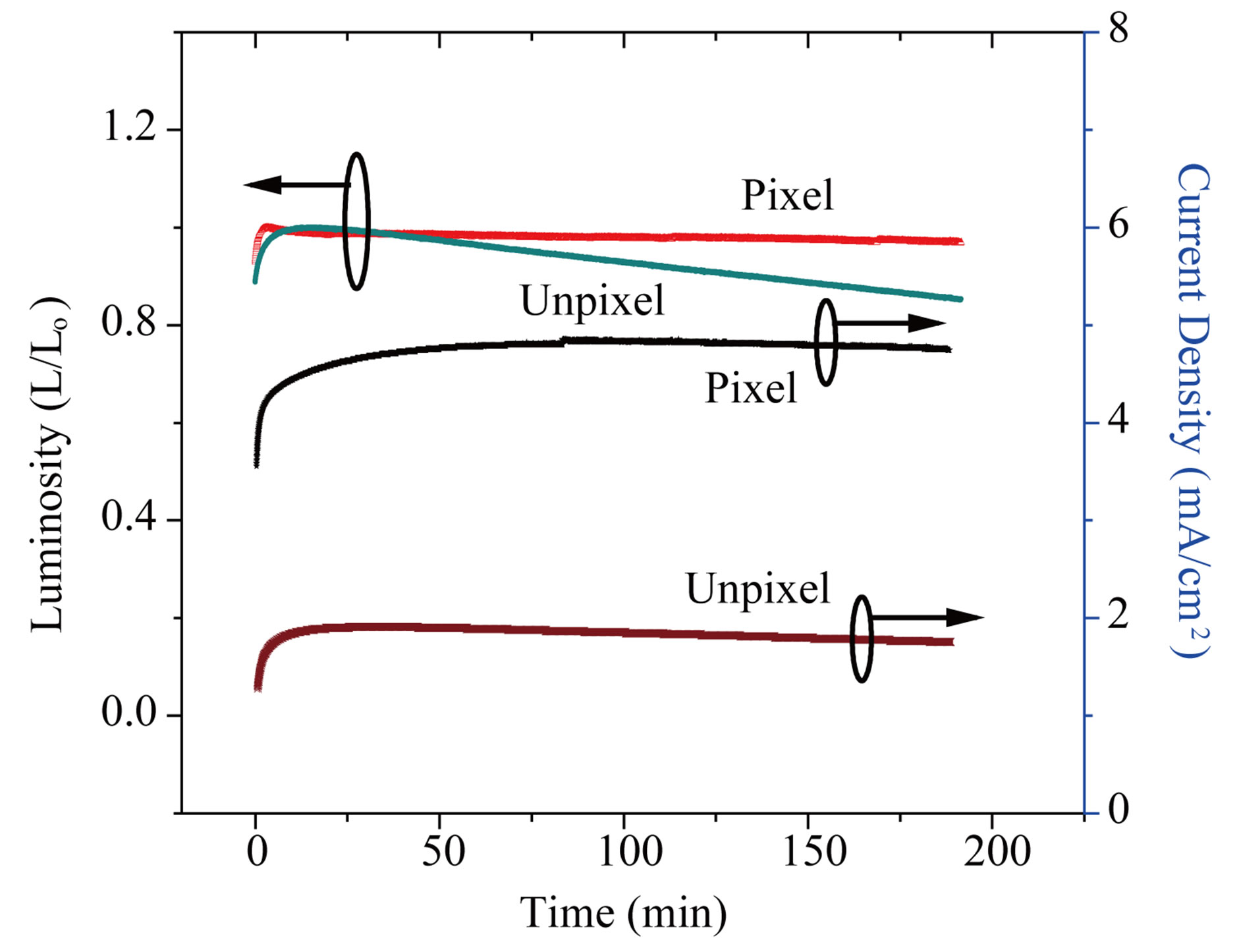
Figure 5. Comparison of luminosity—current density—time (L/Lo- J-t) characteristics for pixellized and unpixellized devices at 5 Volts.
effective number of e-h recombining is enhanced which will result in a higher luminescence.
3.2. Operational Stability of Device
Pixellization with isolation layer also removes the high current density area along the edges and thus will effect the degradation behavior of the devices. When the device has high leakage current, it degrades with high rate due high local fields or high local Joule heating near the sharp edges of ITO. High local fields at the edges of electrode cause hot spots in OLEDs, and consequently result in pinholes in the top electrode as a result oxidation and ablation of the top electrode enhanced [14]. Figure 5 clearly shows that unpixellized devices degrade at much faster rate compare to the pixellized devices. The current flowing through the device is almost constant for the pixellized one but for unpixellized device there was a reduction in current which is due to the degradation of the emissive layer.
4. Conclusions
Insertion of an isolation layer at the edge of ITO anode:
1) Effectively reduces the leakage current, so as to prevent the generation of excess heat, and hence led to the better stability of devices;
2) We also see an enhancement in luminance efficiency due to isolation layer of devices.
REFERENCES
- N. K. Patel, S. Cina and J. H. Burroughes, “High-Efficiency Organic Light-Emitting Diodes,” IEEE Journal of Selected Topics in Quantum Electronics, Vol. 8, No. 2, 2002, pp. 346-361. doi:10.1109/2944.9991059
- Q. Xu, J. Ouyang, Y. Yang, T. Ito and J. Kido, “Ultrahigh Efficiency Green Polymer Light-Emitting Diodes by Nanoscale Interface Modification,” Applied Physics Letter, Vol. 83, No. 23, 2003, pp. 4695-4697. doi:10.1063/1.1630848
- S. Shi and D. Ma, “NaCl/Ca/Al as an Efficient Cathode in Organic Light-Emitting Devices,” Applied Surface Science, Vol. 252, No. 18, 2006, pp. 6337-6341. doi:10.1016/j.apsusc.2005.08.036
- S. H. Kim, J. Jang and J. Y. Lee, “Efficient Electron Injection in Organic Light-Emitting Diodes Using Lithium Quinolate/Ca/Al Cathodes,” Applied Physics Letter, Vol. 91, No. 10, 2007, pp. 103501-103503. doi:10.1063/1.2779105
- L. S. Hung, C. W. Tang and M. G. Mason, “Enhanced Electron Injection in Organic Electroluminescence Devices Using an Al/LiF Electrode,” Applied Physics Letters, Vol. 70, No. 2, 1996, pp. 152-154. doi:10.1063/1.118344
- S. H. Kim, J. Jang and J. Y. Lee, “Improvement in Power Efficiency in Organic Light Emitting Diodes Through Intermediate Mg:Ag Layer in LiF/Mg:Ag/Al Cathodes,” Electrochemical and Solid-State Letters, Vol. 10, No. 10, 2007, pp. J117-J119. doi:10.1149/1.2756337
- L. S. Hung and S. T. Lee, “Electrode Modification and Interface Engineering in Organic Light-Emitting Diodes,” Materials Science and Engineering: B, Vol. 85, No. 2-3, 2001, pp. 104-108. doi:10.1016/S0921-5107(01)00539-6
- R. Singh and M. Katiyar, “Polysilane Based Ultraviolet Light-Emitting Diodes with Improved Turn-On Voltage, Stability and Color Purity,” Synthetic Metals, Vol. 160, No. 17-18, 2010, pp. 1892-1895. doi:10.1016/j.synthmet.2010.07.005
- T. H. Yang, F. S. Juang, Y. S. Tsai, W. K. Kuo and M. Yokoyama, “Improvement of Luminance Efficiency by Insertion of Buffer Layers in Flexible Organic Light-Emitting Diodes,” Japanese Journal of Applied Physics, Vol. 45, 2006, pp. 3729-3732. doi:10.1143/JJAP.45.3729
- H. Becker, S. E. Burns and R. H. Friend, “Effect of Metal Films on the Photoluminescence and Electroluminescence of Conjugated Polymers,” Physical Review B, Vol. 56, No. 4, 1997, pp. 1893-1905. doi:10.1103/PhysRevB.56.1893
- P. E. Burrows, V. Bulovic, S. R. Forrest, L. S. Sapochak, D. M. McCarty and M. E. Thompson, “Reliability and Degradation of Organic Light Emitting Devices,” Applied Physics Letters, Vol. 65, No. 23, 1994, pp. 2922-2924. doi:10.1063/1.112532
- J. Liu, Y. Shi, L. Ma and Y. Yang, “Device Performance and Polymer Morphology in Polymer Light Emitting Diodes: The Control of Device Electrical Properties and Metal/polymer Contact,” Journal of Applied Physics, Vol. 88, No. 2, 2000, pp. 605-609. doi:10.1063/1.373799
- Y. Luo, H. Aziz, Zoran D. Popovic and G. Xu, “Degradation Mechanisms in Organic Light-Emitting Devices: Metal Migration Model versus Unstable Tris(8-Hydroxyquinoline) Aluminum Cationic Model,” Journal of Applied Physics, Vol. 101, No. 3, 2007, pp. 34510-34513. doi:10.1063/1.2435070
- P. E. Burrows, V. Bulovic, S. R. Forrest, L. S. Sapochak, D. M. McCarty and M. E. Thompson, “Reliability and Degradation of Organic Light Emitting Devices,” Applied Physics Letters, Vol. 65, No. 23, 1994, pp. 2922-2924. doi:10.1063/1.112532
- M. Fujihira, L. M. Do, A. Koike and E. M. Han, “Growth of Dark Spots by Interdiffusion across Organic Layers in Organic Electroluminescent Devices,” Applied Physics Letters, Vol. 68, No. 13, 1996, pp. 1787. doi:10.1063/1.116667
- C. H. Chung, T. S. Li, F. S. Juang and D. S. Liu, “Effects of Isolation-Layer on Luminance Efficiency of Organic Light-Emitting Diodes,” Piers Online, Vol. 3, No. 6, 2007, pp. 829-831. doi:10.2529/PIERS061010103344
NOTES
*Corresponding author.