Journal of Crystallization Process and Technology
Vol.3 No.3(2013), Article ID:33871,6 pages DOI:10.4236/jcpt.2013.33013
Investigation of the Solar Cells with Films of Porous Silicon and β-Diketonates
![]()
Institute of Information and Social Technologies, Classic Private University, Zaporozhye, Ukraine.
Email: serg_992000@mail.ru
Copyright © 2013 Sergii Leonidovych Khrypko. This is an open access article distributed under the Creative Commons Attribution License, which permits unrestricted use, distribution, and reproduction in any medium, provided the original work is properly cited.
Received July 5th, 2012; revised August 6th, 2012; accepted August 15th, 2012
Keywords: Silicon; Anodization; Porous; Films; β-diketonates
ABSTRACT
The experimental results of a research of the solar cells parameters covered with films InxSnyOz, and solar cells covered with films, obtained by dispersion of alcoholic solutions of three-chloride Indium acetyl acetonate of aluminum are represented. The spectral dependencies of reflection factor and open circuit voltage of the film-covered solar cells are obtained. The conditions of deriving and properties of porous silicon and parameters of the solar cells with films of porous silicon and covers, forming a potential barrier, are investigated. It is shown that for optimum parameters of films deriving the solar cells with efficiency 15.8% is possible.
1. Introduction
The silicon is one of the base semiconductors of modern semiconductor solar power engineering. One of perspective directions of researches connected with a raise of effectiveness of Sun radiation transformation in an electrical energy, is the development of the photoelectric converters of structures semiconductor-dielectric-semiconductor [1,2]. Such solar cells differ by high effectiveness of photoelectric transformation, simplicity of a construction and process engineering, small power consumption. However, here there is a series, of the physical and engineering tasks, on which successful solution in many respects the scales of use of the researched solar cells in semiconductor engineering will depend.
With the purpose of sufficing the requirements on a raise of efficiency and maximum diminution of losses on a reflection in the field of spectral sensitivity of the solar element use covers of SnO2. In2O3, InxSnyOz, ZnO etc. [3-7]. The width of a forbidden zone of these materials makes about 3.0 - 3.65 eV. Therefore, these materials are transparent for a greater part of a solar radiation. Their factor of a refraction is in limits 1.6 - 2.1 and they can be used together with many semiconductors. Besides optimum selected λ/4—anti reflecting cover can reduce factor of a reflection for given wave length almost up to zero. For deriving a zero reflection in an interval of wave lengths use multilayer anti reflecting of cover.
Except the listed above materials, a film of porous silicon, that have an index of refraction of the order 1.95 ± 0.05, can be used as anti reflecting cover. The cover from porous silicon reduces optical losses in silicon from 37% up to 8% that actually coincides with effectiveness of cover from SiO, obtained in the evaporation in vacuum. Due to a high porosity of cover it is necessary to expect magnification of a current of a short-circuit, open circuit voltage and efficiency of the photoelectric converters.
The purpose of work is the research of a structure and electro-physical performances of film covers for different conditions of their manufacture and influence of these performances to basic parameters of the photoelectric converters.
2. Experimental
The research were fulfilled on slices of the silicon which has been brought up on a Czochralski method, p-type conductivity, boron doped with a resistivity of 0.5 Ohm∙cm and n+-type conductivity, antimony doped with a resistivity of 0.01 Ohm∙cm. The porous silicon films were created by anode handling of a front face of silicon HF-electrolyte. The density of an anode current varied from 1.0 to 30 mA/cm2. The time of anode handling did not exceed 10 minutes. Intensity of illumination for anode handling of n-type conductivity specimens was made 20 mWt/sm2 [8-10]. For security of uniform of an anodization on reverse side or silicon specimens were evaporated films of aluminum (98% Al + 2% Si), which then were annealed at the temperature of 575˚C. The micro-contour of a porous silicon film surface was investigated with optical and electronic microscopy. The thickness of porous silicon films was determined by an oblique grind method. The density of porous silicon was calculated:
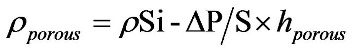 (1)
(1)
where ρSi = 2.33 gramme/cm3—density of monocrystal line silicon; ΔP—alteration of a sample weight after anode handling (gramme); S—surface area of a silicon slice subjected to anode handling (cm2); hporous—thickness of a porous silicon film (cm).
The InxSnyOz films were formed on a front face of silicon specimens by pulverization of InCl3:SnCl4(5H2O): H2O:CH3CH2OH alcoholic solution in a weight relation 34:1:150:150. The temperature of specimens was 430˚C. The thickness of covers depends on time of covering and was 500 - 1500 Å.
The solar cells were produced by sequential covering of a porous silicon film and film InxSnyOz on a surface of silicon specimens. The contacts were created by vacuum evaporation of In-Cu-Cr film. The radiation power on a surface was l00 mWt/cm2, and active area of the solar element was 8.82 cm2.
The surface resistance of InxSnyOz films, their spectral dependencies, and influence of film parameters on current-voltage plot of the solar cells were investigated.
3. Result and Discussion
3.1. Properties of Porous Silicon Films
The dependencies of a thickness of porous silicon films from time of anode handling in 15% a solution HF for slices n+-type are represented on figure 1. This figure shows that the thickness of a porous silicon film will increase linearly with magnification of the anode handling process duration. The plot slope is increased with growth of a density of the anode current. Also the growth rate of porous silicon films will increase linearly in indicated interval and makes for plot 1—4.3 nm/s, plot 2—4.2 nm/s, plot 3—19.0 nm/s, plot 4—21.6 nm/s.
Figure 2 shows the dependencies of a thickness of the porous silicon films obtained on samples of silicon of a p-type with a resistivity 0.5 Ohm∙cm from times of anode handling in the concentrated HF (49%). For these conditions of handling the growth rate of a porous silicon film makes for plot 1—2.2 nm/s, plot 2—10.8 nm/s, plot 3—15.0 nm/s, plot 4—18.3 nm/s, plot 5—21.4 nm/s.
The linearity of a dependence of a porous silicon film thickness from time of an anodization testifies the con-
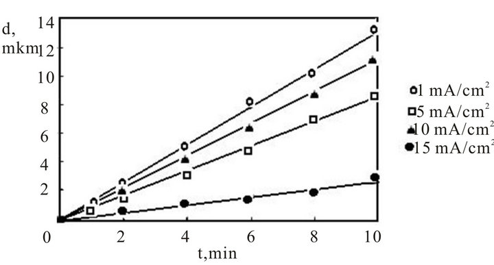
Figure 1. Dependence of thickness of a film porous silicon from time of anodic processing in 15% a solution fluoride of an acid and density of an anodic current (mA/cm2). Specific resistance samples of a n+-type—0.01 Ohm∙cm.
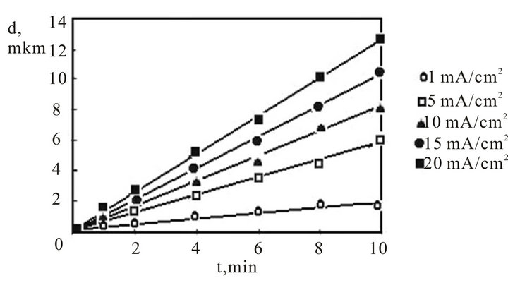
Figure 2. Dependence of thickness of a film porous silicon from time of anodic processing in 49% a solution fluoride of an acid and density of an anodic current (mA/cm2). Specific resistance samples of a p-type—0.5 Ohm∙cm.
stant growth rate of a film with constant density of anode current.
The observed magnification of growth rate is connected with increasing of a density of anode current with magnification of the dissolved silicon amount in accordance with magnification of an amount of solution ions that participates in a current. The process of formation of porous silicon is determined mainly by two factors: by delivery of F ions in reaction zone with formation of silicon fluoride and presence of a positive sign charge carriers, in surface layer of the silicon anode. Therefore, a process of anode handling of nand p-type silicon differs due to difference in concentration of mobile positive charge carriers.
As in acceptor, doped silicon holes are the basic charge carriers and their concentration in a considered case is sufficient for a reaction:
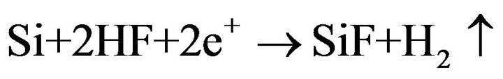
running, so the basic influence on the anodization renders the mechanism of F ions delivery. In donor, doped silicon the holes concentration is small. Therefore, the exterior stimulating factor is necessary for anodization running.
Figure 3 shows the experimental dependencies of a volumetric density of porous silicon obtained by handling n+-specimens in 15% HF solution, from a density of anode current.
The figure shows that the increasing of thickness of a porous silicon film causes describing of material density, which characterizes the structure of the material: Thus, there is possibility to operate by structure of porous silicon with changing conditions of anode handling.
The study of porous silicon structure shows, that the magnification of a current density causes the increasing of the amorphous phase part in material. The REM establishes analysis of a surface with various volumetric densities, that there are reflexes, which correspond to crystallographic planes for samples with curves one, two and tree on figure 3.
However, on the REM data there are no Kikuchi lines that generally appear for monocrystalline silicon. A dependence of a volumetric density of p-type porous silicon from thickness of layer and the densities of anode current are represented on figure 4. The figure shows, that in a researched range of current densities and thicknesses the volumetric density vanes unsignificantly, that testifies to homogeneity of the process of dissolution of silicon. The pores diameter for investigated samples was.
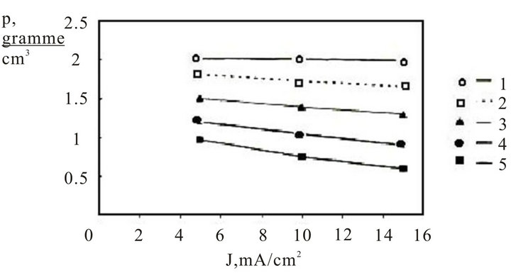
Figure 3. Dependence of volumetric density of porous n+ -type silicon from density of anode current for different thickness of films (mkm): 1: 1.0; 2: 2.0; 3: 4.0; 4: 6.0; 5: 8.0.
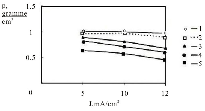
Figure 4. Dependence of volumetric density of porous ptype silicon from density of anode current for different thickness of films (mkm): 1: 1.0; 2: 2.0; 3: 4.0; 4: 6.0; 5: 8.0.
40 - 210 Å, and number of pores—4 × 10⁸ - 8 × 109 cm2. The size of pores will increase with magnification of a current density, time of anode handling and thickness of a porous silicon film.
The number of pores is maximum for pores with 40 - 80 Å diameter. The further magnification of a diameter of pores happens not only due to dissolution of silicon on the pores walls, but also at the expense of secondary effect of join small-sized, close located pores (Figure 5).
3.2. Properties of Films InxSnyOz
Figure 6 shows the dependence of the turn InxSnyOz surface resistance from percentage SnCl4(5H2O) in a solution. The least magnitude of a surface resistance has the samples with an In2O3 film. Increasing of a SnCl4 (5H2O) content causes the rise of surface resistance from 20 up to 600 Ohm/cm2. It may be explained, apparently, by substituting of In atoms by small amounts of tin, that representing itself as the donors. However, with SnCl4 (5H2O) content increasing the content of SnO2 phase in InxSnyOz film structure grows, that reduces the charge carriers concentration and material conductivity.
To reduce magnitude of oxide metal cover surface resistance one can use β-diketonates, for example acetil acetonate of aluminium Al(AA)3. Al(AA)3 was obtained from a solution of AlCl3∙6H2O, is rectified by zone method and had such crystal and chemical characteristics: coordination of a metal ion-octahedron; space group— P21/c; syngony-monocline; parameters of a lattice—a = 14.16 Å, b = 7.48 Å, c = 16.43 Å, β = 98˚. The InxAlyOz films were obtained by thermal decomposition on the heated surface of silicon (up to 470˚C) substrate in inert gas stream with adding of an oxidizer. The surface resistance of a film decreases and makes 7 - 10 Ohm/cm2. (figure 6, curve 2).
The spectral dependencies of InxSnyOz films reflection factor of a various thickness were investigated. The results are represented on figure 7. The least reflection of

Figure 5. Morphology porous p-type silicon.

Figure 6. Dependence of InxSnyOz films surface resistance from SnCl4(5H2O) contents in solution (1) and InxAlyOz films surface resistance from A1(AA)3 contents in gas phase (2).
radiation quantum’s have the InxSnyOz films with thickness of 650 - 750 Å. The enlightenment is most hardly appears in a spectral range of 0.5 - 0.8 microns. The InxSnyOz film more clarifies a surface of silicon, than the film of SiO2. In the field of a maximum enlightenment for specimens with InxSnyOz films, the reflection factor is reduced up to.
On the surface of silicon, substrate for normal conditions of an environment the film atmospheric SiOx grows. Strictly speaking, in this case on the surface of silicon the structure InxSnyOz/SiOx/Si is created.
Preoxidizing handling included growth of oxide by a thickness 5000 Å (T = 900˚C in a damp atmosphere). Then that oxide was etching and the silicon slices were washed in a boiling solution (H2O2:NH4OH:H2O = 1:1:4) and deionic water with consequent drying. After daily endurance in air, the thickness of natural oxide was 14 Å, and after endurance within 4 day - 43 Å. The structures InxSnyOz/SiOx after daily endurance in air had a surface resistance of 65 Ohm/cm2, and after endurance during 4 day - 140 Ohm/cm2. Annealing of structures in air at the temperature of 200˚C within 10 minutes reduced the surface resistance from 65 Ohm/cm2 till 75 - 80 Ohm/cm2 and from 140 Ohm/cm2 up to 170 Ohm/cm2. The annealing time about 20 minutes promoted further growth of a surface resistance. Cyclical annealing of InxSnyOz/Si structure in hydrogen and argon at the temperature of 550˚C promoted a drop of InxSnyOz film surface resistance from 20 Ohm/cm2 up to 7 - 8 Ohm/cm2, and film InxAlyOz from 10 Ohm/cm2 up to 3 - 4 Ohm/cm2. During the annealing there is the restoring of oxide and release of metal atoms, therefore, the surface resistance decreases.
3.3. Performances of the Photoelectric Converters
It must be matched such condition for high effectiveness of the photo-electric converters with semiconductor dielectric-semiconductor structures: the width of a forbidden zone (Eg) of cover, that forms a potential barrier,
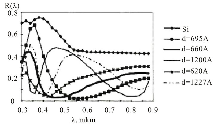
Figure 7. Spectral dependences of reflection factor of a InxSnyOz films with various thickness.
should be ≥3.0 eV and this semiconductor should be degenerate. In case of a base semiconductor of p-type, work function (A) of semiconductor cover, forming a barrier, and value electron affility of a base semiconductor (χs) should satisfy to a relation A < (χs). In case of a base semiconductor of n-type the validity of a relation A > χs + Eg is necessary. The mismatch of lattice constants should be minimum. In table 1 some data on a relation between A, χs and Eg for some semiconductor covers forming on silicon a potential barrier are represented.
These data show, that optimum pairs for silicon of p-type are In2O3, InxSnyOz, ZnO, CdO. For silicon of ntype optimum cover forming a barrier is SnO2.
The important parameters of semiconductor covers are a thickness and temperature of covering. Figure 8 shows the spectral performances of the photoelectric converters InxSnyOz/SiOx/pSi with the InxSnyOz thickness of 800 Å, and temperature of covering from 350˚C to 550˚C. The optimal temperatures of InxSnyOz covering are 400˚C - 425˚C. The maximum magnitude of open circuit voltage is achieved for wave length of 0.7 microns.
Figure 9 shows the similar spectral performances for the InxSnyOz/SiOx/nSi photoelectric converters. For all the specimens time between drying and covering by semiconductor layer, that forming a potential barrier, did not exceed 10 minutes. The Figure shows, that in a range of temperatures 400˚C - 425˚C a range of wave lengths, in which the high values of open circuit voltage are observed, was narrowed down from 0.65 microns to 0.85 microns and open circuit voltage have decreased. It confirms a high compatibility of InxSnyOz/SiOx/pSi structures.
The spectral characteristics of photoelectric converters with structures InxSnyOz/SiOx/nSi, InxSnyOz/SiOx/porousSi/ nSi,InxAlyO/SiOx/porousSi/nSi arc submitted on figure 10.
The thickness of silicon film −0.7 - 4.5 microns. The best spectral performances have InxSnyOz/SiOx/porous Si/nSi, InxAlyO/SiOx/porousSi/nSi structures. In addition, the curve (2) shifts more in long wavelength area of
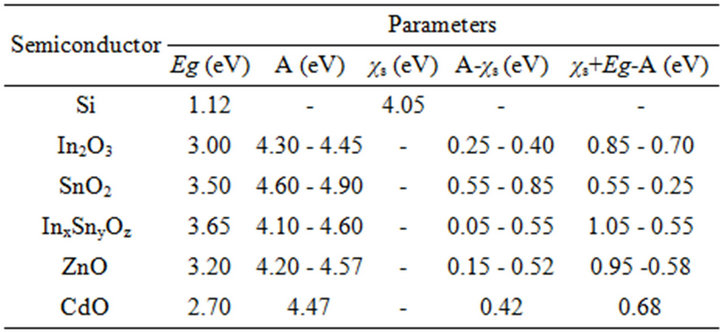
Table 1. Parameters of semiconductors forming potential barrier with silicon.
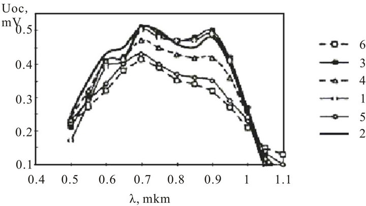
Figure 8. The spectral characteristics of InxSnyOz/SiOx/pSi photoelectric converters: 1: 350˚C; 2: 400˚C; 3: 425˚C; 4: 425˚C; 5: 500˚C; 6: 550˚C.
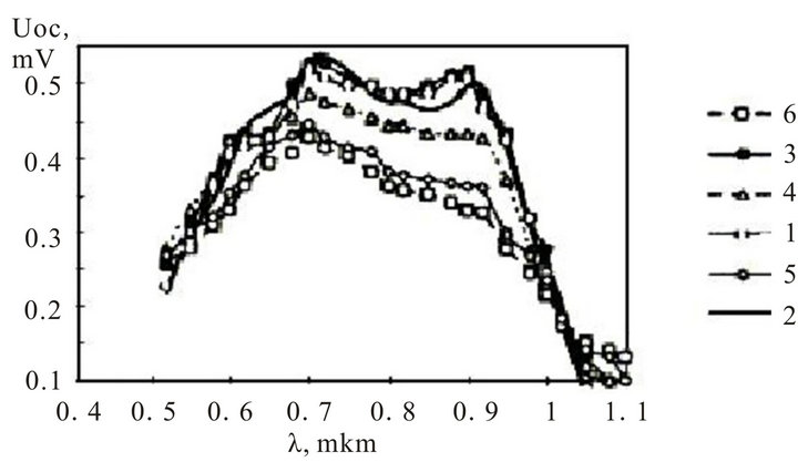
Figure 9. The spectral characteristics of InxSnyOz/SiOx/nSi photoelectric converters: l: 350˚C; 2: 400˚C; 3: 425˚C; 4: 445˚C; 5: 500˚C; 6: 550˚C.
a spectrum, and curve (3) in short wave.
The experimental light current-voltage characteristics of the silicon photoelectric converters with various covers are represented on figure 11, and the basic parameters are shown in table 2. These data testify, that for investigated structures the acceptable efficiency are obtained and they are perspective structures for a photo electric converters.
4. Summary
We have demonstrated that the covers, forming a potential barrier, can be successfully used for creation of the
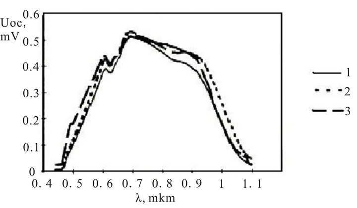
Figure 10. The spectral characteristics of photoelectric converters with structure: 1) InxSnyOz/SiOx/nSi; 2) InxSnyOz/ SiOx/porousSi/nSi; 3) InxAlyO/SiOx/porousSi/nSi.
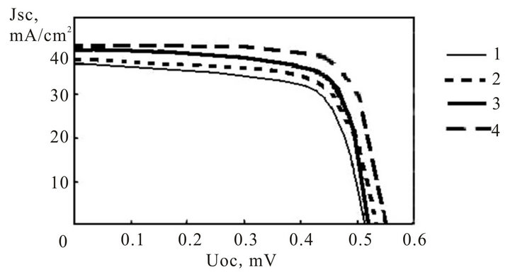
Figure 11. Current-voltage characteristics of photoelectric converters with structure: 1) InxSnyOz/SiOx/nSi; 2) InxSnyOz/SiOx/porousSi/nSi; 3) InxAlyO/SiOx/porousSi/nSi; 4) InxSnyOz/SiOx/porousSi/pSi.
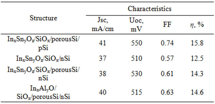
Table 2. The characteristics of photoelectric converters.
effective solar cells. Especially the covers with β- diketonates are effective. The creation of a developed porous surface on silicon slices considerably increases absorption of light and improve parameters of the photoelectric converters.
REFERENCES
- L. S. Berman, E. I. Beliakova, L. S. Kostina, E. D. Kim and S. C. Kim, “An Analysis of Charges and Surface States at the Interfaces of Semiconductor-Insulator-Semiconductor Structures,” Semiconductors, Vol. 34, No. 7, 2000, pp. 786-789.
- J. Shewchum, D. Druk and R. Siughetal, “The Semiconductor-Insulator-Semiconductor (Indium Tin Oxide on Silicon) Solar Cell: Characteristics and Loss Mechanisms,” Journal of Applied Physics, Vol. 50, No. 10, 1979, pp. 6524-6533. doi:10.1063/1.325749
- H. H. Afify, S. H. El-Hefnawi, A. Y. Eliwa, M. M. Abdel-Naby and N. M. Ahmed, “Realization and Characterization of ZnO/n-Si Solar Cells by Spray Pyrolisis,” Egyptian Journal of Solids, Vol. 28, No. 2, 2005, pp. 243- 254.
- S. L. Khrypko, “Properties of Thin Transparent SnO2: Sb Films,” Journal of Nanoand Electronic Physics, Vol. 1, No. 1, 2009, pp. 92-98.
- S. L. Khrypko, “Investigation of the Solar Cells with Films of Porous Silicon,” Photoelectronics, No. 17, 2008, pp. 45-50.
- G. K. Zholudev and S. L. Khrypko, “Effect of Hydrochloric Acid on Mechanisms of Porous Silicon,” Physics and Chemistry of Solids, Vol. 10, No. 1, 2009, pp. 149- 156.
- R. Bilyalov, A. Ulyashin; M. Scherff, K. Meusinger, J. Poortmans and W. Fahrner, “P-Type Silicon Heterojunction Solar Cells with Different Interfaces and Surface Structures,” Proceedings of 3rd World Conference Photovoltaic Energy Conversion, Osaka, 12-16 May 2003, pp. 1139-1142.
- K. Kordas, S. Beke, A. E. Pap, A. Uusimaki and S. Leppavuori, “Optical Properties of Porous Silicon,” Optical Materials. Part II: Fabrication and Investigation of Multiplayer Structures, Vol. 25, No. 3, 2003, pp. 257-260.
- W. Suntao, W. Yanhua and S. Qihua, “Measurement and Analysis of the Characteristic Parameters for the Porous Silicon/Silicon Using Photovoltage Spectra,” Applied Surface Science, Vol. 158, No. 3-4, 1999, pp. 268-274. doi:10.1016/S0169-4332(00)00008-8
- E. Pincik, P. Bartos and M. Jergel, “The Metastability of Porous Silicon-Crystalline Silicon Structure,” Thin Solid Films, Vol. 343-344, 1999, pp. 277-280. doi:10.1016/S0040-6090(98)01572-7