Journal of Modern Physics
Vol.05 No.18(2014), Article ID:52764,7 pages
10.4236/jmp.2014.518212
Study of Optical and Electrical Properties of Nickel Oxide (NiO) Thin Films Deposited by Using a Spray Pyrolysis Technique
Ahmed J. Hassan
Department of Physics, College of Science, University of Thi-Qar, Thi-Qar, Iraq
Email: Ahmed.jhassan@yahoo.com
Copyright © 2014 by author and Scientific Research Publishing Inc.
This work is licensed under the Creative Commons Attribution International License (CC BY).
http://creativecommons.org/licenses/by/4.0/


Received 25 October 2014; revised 21 November 2014; accepted 18 December 2014
ABSTRACT
Nickel oxide (NiO) thin film has been deposited on a glass substrate at a temperature of 390˚C ± 10˚C using a simple and inexpensive spray pyrolysis technique. Nickel nitrate salt solution (Ni(NO3)2∙6H2O) was employed to prepare the films and the film thickness was in order of 200 ± 5 nm. The structural, optical and electrical properties of NiO films were investigated using X-ray diffraction (XRD), visible spectrum, DC conductivity and Seebeck effect measurements. The results show that X-ray diffraction techniques have shown that prepared film is polycrystalline struc- ture type cubic phase. The measurements of optical properties (transmittance (T) and absor- bance (A)) of NiO films show that higher transmittance is 37.4% within the wavelength range (300 - 900 nm). Also the results have shown that the higher absorbance is 77.7%. The results of electrical properties have shown that at room temperature electrical conductivity is 1.3 × 10⁻⁵ (Ω∙cm)−1, and also results have shown that all the films are of p-type due to the negative Seebeck coefficient.
Keywords:
Nickel Oxide, Spray Pyrolysis Technique

1. Introduction
NiO is a well-known antiferromagnetic material [1] , and a metal-deficient p-type semiconductor [2] with a 3.6 eV band gap [3] . Nickel oxide (NiO) films have a wide range of applications due to their excellent chemical stability. They have been used as catalysts [4] , electrochromic display devices [5] , fuel cells [6] and gas sensors [7] . The nickel oxide thin films have been prepared using various techniques including thermal evaporation [8] , spray pyrolysis [9] , chemical vapor deposition [10] , electrochemical deposition [11] , sol-gel [12] [13] , sputtering [14] [15] , chemical solution deposition [16] [17] , etc. All these methods offer different advantages depending on the application of interest and many efforts have been conducted to obtain films with the desirable physical and/or chemical properties. Among the different methods for film deposition, the relative simplicity of the spray pyrolysis method and its potential application for large area deposition make it very attractive and feasible for mass production processes [18] . Although SPT has been employed in the past to deposit NiO films through acetylacetonate [19] and nitrate [20] routes, their characterization has sparsely been carried out. Aqueous solutions are commonly used in the SP system to deposit thin films due to ease of handling, safety, low cost and availability of a wide range of water-soluble metal salts [21] .
2. Experimental Procedure
Nickel oxide thin films were prepared by spraying a 0.1 M solution of nickel nitrate of doubly distilled water onto the pre-heated amorphous glass substrates kept at 390˚C ± 10˚C. Film thickness was measured by using the weight difference method considering the density of the bulk nickel oxide. As the density of thin films was certainly lower than the bulk density, the actual film thickness would be larger than the estimated values. The structural, optical and electrical characterization of the films deposited at optimized preoperative parameters was carried out. The X-ray diffractometer (Shimadzu 6000) Target: CuKα, Voltage 40 KV, Current 30 MA. Where λ is the X-ray wavelength (1.54060 Å). The optical measurements comprise measuring the absorbance and transmittance with range (300 - 900 nm), in the current study, by using (UV-1650PC Shimadzu software 1700, 1650, UV-visible recording spectrophotometer). A two-probe resistivity unit was used to measure the electrical resistivity of the films in the temperature range) 30˚C - 170˚C). Thermoelectric power is an effective method for estimating the type of charge carrier (n-type or p-type) especially those materials of large energy gap and transport mechanism in polycrystalline semiconductors.
3. Results and Discussions
The nickel oxide thin films were analyzed by X-ray diffraction technique to study the structural identification and changes in the crystalline. The XRD patterns of nickel oxide thin film are shown in Figure 1. It is found that

Figure 1. The X-ray diffractograms of NiO films.
the film was polycrystalline consisting of one cubic phase, comprising a strong reflection along (111) plane. By comparing the XRD pattern with the JCPDS data, it was found that the product is nickel oxide (JCPDS file no: 73-1519). Also The prepared film, which agrees with that in the literatures P. S. Patil and L. D. Kadam, (2002) [21] V. Patil, et al. (2011) [22] H. L. Chen, et al. (2005) [23] and I. Fasaki, et al. [24] . The diffragram of the new film shows one pronounced diffraction peaks, (111) appear at 2θ = 28.001˚. The X-ray result shows that the film was crystallized in the cubic phase with polycrystalline structure.
4. Optical Properties
In studying the varied spectrum of transmittance, absorbance and reflectance for these films, we can calculate many optical constants, like absorption coefficient, and allowed and forbidden energy gap for direct translations.
4.1. Transmittance (T)
Figure 2 shows the optical transmission as a function of wavelength in the range (300 - 900 nm) for NiO films. The maximum transmittance observed was almost (37.4%). The figures show that the transmittance of film has a high value (more than 32.64%) at (λ > 500 nm), i.e. in visible and near infrared regions. Our result is in good agreement with P. S. Patil and L. D. Kadam, (2002) [21] .
4.2. Absorbance (A)
Figure 3 shows the variety of observance as a function of wavelength, within the range (300 - 900 nm) for NiO film’s investigation. It can be noticed from the figure that the absorbance for films has a high value at wavelengths in the near of the fundamental absorption edge (360 nm). In general the observance of films has low values in the visible and near infrared region, this behavior can be explained as follows, at high wavelength the

Figure 2. Transmittance (%) versus wavelength for NiO films.
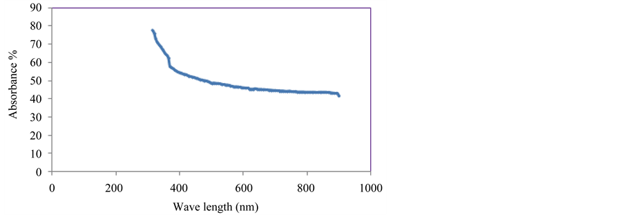
Figure 3. Absorbance versus wavelength for NiO films.
incident photons don’t have enough energy to interact with atoms, the photon will transmitted. When the wavelength decreases, the interaction between incident photon and material will occur, and then the absorbance will increase.
4.3. Reflectance (R)
Reflectance is defined as the ratio of the reflected intensity rays to the value of the intensity of incident rays. Reflectivity can be calculated from absorption and transmission spectrum in accordance to the law of conservation of energy by the relation [25] .
 (1)
(1)
where: R: is the reflectance; T: is the transmittance; and A: is the absorbance.
The change of reflectance as a function of wavelength is shown in Figure 4 of films. The figure shows that the reflectance of films is extremely low in the visible region and it increases with decreasing of wavelength. The behavior of reflectance is in agreement with the behavior of transmittance and absorbance according to Equation (1).
4.4. Absorption Coefficient Measurements: (α)
The absorption coefficient (α) has been calculated from Equation (2). This coefficient depends on the incident photon energy (hυ), the energy gap of semiconductors and the type of the electronic transitions. Figure 5 shows the change of the absorption coefficient of films as a function of incident photon energy. It is observed that the absorption coefficient (α) increases gradually with the incident photon energy, and that value is greater than (104 cm−1) which indicates the strong possibility of direct electronic transitions [26] . Nickel oxide is a high band-gap semiconductor with the absorption edge in the UV region and no absorption in the visible region [21] .

Figure 4. Reflectance versus wavelength for NiO films.

Figure 5. Absorption coefficient versus photon energy for NiO films.
 (2)
(2)
where: α is absorption coefficient, A is the absorbance, it is the thickness of the film.
4.5. Optical Energy Gap
From the transmittance and absorption data and according to relation, (αE)2 versus incident photon energy, (E), plots were obtained. The graphs are represented in Figure 6. The values of band gap can be determined by extraplotting the linear portion of the curve to (αhυ)2 = 0. The band gap energy values are found to be 3.3 eV. Our result is in good agreement with S. A. Mahmoud, et al. (2011) [18] , P. S. Patil and L. D. Kadam, (2002) [21] and V. Patil, et al. (2011) [22] .
5. Electrical Properties
5.1. Electrical Resistivity Measurement
The resistivity of the film depends upon several factors such as the preparation technique, the preparation parameters, the doping agent, the annealing temperature and even the measurement conditions. The resistivity for the deposited thin films was calculated by using Equations (3) at temperature within the range (30˚C - 170˚C) [27] :
 (3)
(3)
where: R is the resistance of the sample (thin film); b is the width of (Al) pole; t is the film thickness; l is the distance between two (Al) poles.
Figure 7 shows the variation of electrical resistivity with temperature for NiO films, it is observed that

Figure 6. (αE)2 versus photon energy for NiO films.

Figure 7. Resistivity versus temperature for NiO films.
resistivity decreases with increase in temperature and supports the semiconducting nature of NiO films. Electrical resistivity of nickel oxide thin films have been studied by many researchers [2] [16] [29] - [31] , and reported resistivity is in the range of 10 - 106 (Ω×cm).
5.2. Activation Energy (DC Conductivity)
Then plotting the relationship of lnσDC versus (1000/T) to determine the activation energy of the conductivity as shown in Figure 8 from the production of the slope (of the plot) by Boltzmann constant in (eV) units as the Equation (4). It has been noticed that in general and in all films that the DC conductivity (σ) increases with increasing the temperature and that is the natural state which means normal property from properties of semiconductors that have a resistance of negative thermal coefficient, whereas the concentration of carriers increase with increasing the temperature [32] . The values of the film activation energy are given in Table 1.
 (4)
(4)
5.3. Thermoelectric Power (Seebeck Measurements)
The measurement of thermoelectrical power as a function of temperature, is one of the most important characteristics of electronics, Seebeck measurements confirmed that NiO films were p-type. The Seebeck coefficient of films was calculated from voltage (mV) versus T (K) plot as shown in Figure 9. The calculated values of Sb are tabulated in Table 1.
5.4. Activation Energy (Thermoelectric Power)
The activation energy (Es) of films was calculated from Sb (mV/K) versus 1000/T (K) plot as shown in Figure 10. The calculated values of (Es) are tabulated in Table 1.
6. Conclusion
From the obtained results of the present work it can be concluded that:
The X-ray result shows that the crystalline structure of (NiO) film is crystallized in the cubic single phase with polycrystalline structure. It is formed and the films show preferential growth along the direction. The best transmittance was 37.4% within the wavelength range (300 - 900 nm), and the highest observance was at wave-

Figure 8. Activation energy for NiO films.

Table 1. Show properties of NiO thin films prepared by spray pyrolysis technique.

Figure 9. Seebeck effect of NiO films.

Figure 10. Activation energy for NiO films.
lengths in the near of the fundamental absorption edge (360 nm) for films. The refractive index reflectance of films is extremely low in the visible region and it increases with decreasing of wavelength, the higher value of the refractive index at λ > 400 nm. It is observed that the absorption coefficient (α) increases gradually with the incident photon energy, and that value is greater than (104 cm−1), and thus the absorption coefficient is largely increased at hυ > 3.5 eV. This converts to a large probability that direct electronic transition will happen. The value of optical energy gap (Eg) values is found to be 3.3 eV. It is observed that resistivity decreases with increase in temperature and supports the semiconducting nature of NiO films. Reported resistivity is in the range of 10 - 106 (Ω×cm). Seebeck measurements confirmed that NiO films were p-type.
Acknowledgements
I extend my thanks to the Head of the Department of Physics at the University of Thi Qar, Prof. Dr. Falah Hassan to help me in completing this research and also to thank my supervisor Prof. Arwaa Fadhel Saleh for standing with me to complete this research.
References
- Fujii, E., Tomozawa, A., Torii, H. and Takayama, R. (1996) Japanese Journal of Applied Physics, 35, L328. http://dx.doi.org/10.1143/JJAP.35.L328
- Sato, H., Minami, T., Takata, S. and Yamada, T. (1993) Thin Solid Films, 236, 27. http://dx.doi.org/10.1016/0040-6090(93)90636-4
- Sasi, B., Gopchandran, K.G., Manoj, P.K., Koshy, P., Prabhakara Rao, P. and Vaidyan, V.K. (2003) Vacuum, 68, 149. http://dx.doi.org/10.1016/S0042-207X(02)00299-3
- Roslik, A.K., Konev, V.N. and Maltsev, A.M. (1995) Oxidation of Metals, 43, 1. http://dx.doi.org/10.1007/BF01046745
- Ahn, K.S., Nah, Y.C. and Sung, Y.E. (2002) Applied Surface Science, 199, 259. http://dx.doi.org/10.1016/S0169-4332(02)00863-2
- Chen, X., Wu, N.J., Smith, L. and Ignatiev, A. (2004) Applied Physical Letters, 84, 2700. http://dx.doi.org/10.1063/1.1697623
- Fasaki, I., Giannoudakos, A., Stamataki, M., Kompitsas, M., György, E., Mihailescu, I.N., Roubani-Kalantzopoulou, F., Lagoyannis, A. and Harissopulos, S. (2008) Applied Physics A, 91, 487. http://dx.doi.org/10.1007/s00339-008-4435-0
- Sasi, B., Gopchandran, K., Manoj, P., Koshy, P., Rao, P. and Vaidyan, V.K. (2003) Vacuum, 68, 149-154. http://dx.doi.org/10.1016/S0042-207X(02)00299-3
- Desai, J.D., Min, S.K., Jung, K.D. and Joo, O.S. (2006) Applied Surface Science, 253, 1781-1786. http://dx.doi.org/10.1016/j.apsusc.2006.03.009
- Kang, J.-K. and Rhee, S.W. (2001) Thin Solid Films, 391, 57-61. http://dx.doi.org/10.1016/S0040-6090(01)00962-2
- Nakaoka, K., Ueyama, J. and Ogura, K. (2004) Journal of Electroanalytical Chemistry, 571, 93-99. http://dx.doi.org/10.1016/j.jelechem.2004.05.003
- Taylor, D.J., Fleig, P.F., Schwab, S.T. and Page, R.A. (1999) Surface and Coatings Technology, 120-121, 465-469. http://dx.doi.org/10.1016/S0257-8972(99)00418-1
- Garcia-Miquel, J.L., Zhang, Q., Allen, S.J., Rougier, A., Blyr, A., Davies, H.O., Jones, A.C., Leedham, T.J., William, P.A. and Impey, S.A. (2003) Thin Solid Films, 424, 165-170. http://dx.doi.org/10.1016/S0040-6090(02)01041-6
- Park, J.W., Park, J.W., Kim, D.Y. and Lee, J.K. (2005) Journal of Vacuum Science & Technology A, 23, 1309-1313. http://dx.doi.org/10.1116/1.1953687
- Chen, H.L., Lu, Y.M. and Hwang, W.S. (2005) Thin Solid Films, 514, 361-365. http://dx.doi.org/10.1016/j.tsf.2006.04.041
- Pramanik, P. and Bhattacharya, S. (1990) Journal of the Electrochemical Society, 137, 3869-3870. http://dx.doi.org/10.1149/1.2086316
- Banerjee, S., Santhanam, A., Dhathathrenyan, A. and Rao, P.M. (2003) Langmuir, 19, 5522-5525. http://dx.doi.org/10.1021/la034420o
- Mahmoud, S.A., Alshomer, S. and Tarawnh, M.A. (2011) Journal of Modern Physics, 2, 1178-1186. http://dx.doi.org/10.4236/jmp.2011.210147
- Xie, Y., Wang, W., Qian, Y., Yang, L. and Chen, Z. (1996) Journal of Crystal Growth, 167, 656-659. http://dx.doi.org/10.1016/0022-0248(96)00285-0
- Misho, R.H., Murad, W.A., Fatahalah, G.H., Abdul-Aziz, I.M. and Al-Doori, H.M. (1988) Physica Status Solidi (a), 109, K101-K104. http://dx.doi.org/10.1002/pssa.2211090237
- Patil, P.S. and Kadam, L.D. (2002) Applied Surface Science, 199, 211-221. http://dx.doi.org/10.1016/S0169-4332(02)00839-5
- Patil, V., Pawar, S., Chougule, M., Godse, P., Sakhare, R., Sen, S. and Joshi, P. (2011) Journal of Surface Engineered Materials and Advanced Technology, 1, 35-41. http://dx.doi.org/10.4236/jsemat.2011.12006
- Chen, H.L., Lu, Y.M. and Hwang, W.S. (2005) Surface and Coatings Technology, 198, 138-142. http://dx.doi.org/10.1016/j.surfcoat.2004.10.032
- Fasaki, I., Koutoulaki, A., Kompitsas, M. and Charitidis, C. (2010) Applied Surface Science, 257, 429-433. http://dx.doi.org/10.1016/j.apsusc.2010.07.006
- Eckortova, L. (1977) Physics of Thin Films. Plenum Press, New York.
- Pankove, J. (1969) Optical Processes in Semiconductors. Prentice-Hall, Inc., Upper Saddle River.
- Strectman, G.B. and Banerjee, S. (2000) Solid State Electronic Devices. 5th Edition, Prentice Hall, Englewood Cliffs.
- Varkey, A.J. and Fort, A.F. (1993) Thin Solid Films, 235, 47-50. http://dx.doi.org/10.1016/0040-6090(93)90241-G
- Kadam, L.D., Bhosale, C.H. and Patil, P.S. (1997) Turkish Journal of Physics, 21, 1037.
- Adler, D., Tjeng, L.H., Voogt, F.C., Hibma, T., Sawatzky, G.A., Chen, C.T., Vogel, J., Sacchi, M. and Iacobucci, S. (1998) Physical Review B: Condensed Matter and Materials Physics, 57, 11623. http://dx.doi.org/10.1103/PhysRevB.57.11623
- Davazoglou, D., Leveque, G. and Donnadieu, A. (1988) Solar Energy Materials, 17, 379-390. http://dx.doi.org/10.1016/0165-1633(88)90020-2
- Chopra, K.L. (1969) Thin Films Phenomena. McGraw-Hill, New York.