Paper Menu >>
Journal Menu >>
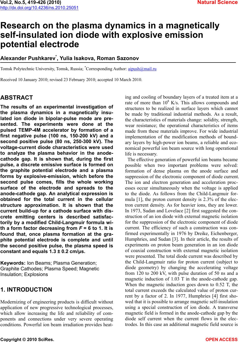 Vol.2, No.5, 419-426 (2010) Natural Science http://dx.doi.org/10.4236/ns.2010.25051 Copyright © 2010 SciRes. OPEN ACCESS Research on the plasma dynamics in a magnetically self-insulated ion diode with explosive emission potential electrode Alexander Pushkarev*, Yulia Isakova, Roman Sazonov Tomsk Polytechnic University, Tomsk, Russia; *Corresponding Author: aipush@mail.ru Received 10 January 2010; revised 23 February 2010; accepted 10 March 2010. ABSTRACT The results of an experimental investigation of the plasma dynamics in a magnetically insu- lated ion diode in bipolar-pulse mode are pre- sented. The experiments were done at the pulsed TEMP-4M accelerator by formation of a first negative pulse (100 ns, 150-200 kV) and a second positive pulse (80 ns, 250-300 kV). The voltage-current diode characteristics were used to analyze the plasma behavior in the anode- cathode gap. It is shown that, during the first pulse, a discrete emissive surface is formed on the graphite potential electrode and a plasma forms by explosive-emission, which before the second pulse comes, fills the whole working surface of the electrode and spreads to the anode-cathode gap. An analytical expression is obtained for the total current in the cellular structure approximation. It is shown that the current build-up for a cathode surface with dis- crete emitting centers is described satisfac- torily by a modified Child-Langmuir formula wi- th a form factor decreasing from F = 6 to 1. It is found that, once plasma formation at the gra- phite potential electrode is complete and until the second positive pulse, the plasma speed is constant and equals 1.3 ± 0.2 cm/μs. Keywords: Ion Beams; Plasma Generation; Graphite Cathodes; Plasma Speed; Magnetic Insulation; Explosions 1. INTRODUCTION Modernizing of engineering products is difficult without application of new progressive technological processes, which allow increasing the life and reliability of com- ponents and connections under very severe operating conditions. Powerful ion beam irradiation provides heat- ing and cooling of boundary layers of a treated item at a rate of more than 108 K/s. This allows compounds and structures to be realized in surface layers which cannot be made by traditional industrial methods. As a result, the characteristics of materials change: solidity, strength, wear resistance; the operational characteristics of items made from these materials improve. For wide industrial implementation of the modification methods of bound- ary layers by high-power ion beams, a reliable and eco- nomical powerful ion beam source with long operational life is necessary. The effective generation of powerful ion beams became possible when two important problems were solved: formation of dense plasma on the anode surface and suppression of the electronic component of diode current. The ion and electron generation and acceleration proc- esses occur simultaneously when the voltage is applied to the diode. As follows from the Child-Langmuir for- mula [1], the proton current density is 2.3% of the elec- tron current density. As for heavier ions, they are lower. In 1973, Sudan and Lovelace [2] first suggested the con- struction of an ion diode with external magnetic isolation for the suppression of the electronic component of diode current. The efficiency of such a construction was con- firmed experimentally in 1976 by Dreike, Eichenberger, Humphries, and Sudan [3]. In their article, the results of experiments on proton beam generation in an ion diode of coaxial construction with external magnetic isolation were presented. The total diode current was described by the Child-Langmuir ratio for proton current (subject to diode geometry) by changing the accelerating voltage from 120 to 200 kV, with pulse duration of 50 ns and a magnetic induction of 1.03 T in the anode-cathode gap. When the magnetic induction goes down to 0.52 T, the total current exceeds the calculated value of proton cur- rent by a factor of 2. In 1977, Humphries [4] first sho- wed that it is possible to arrange magnetic self-insulation using a special construction of ion diode. A transverse magnetic field is formed in the anode-cathode gap by the diode self current when the current flows in the elec- trodes. In this case an additional magnetic field source is 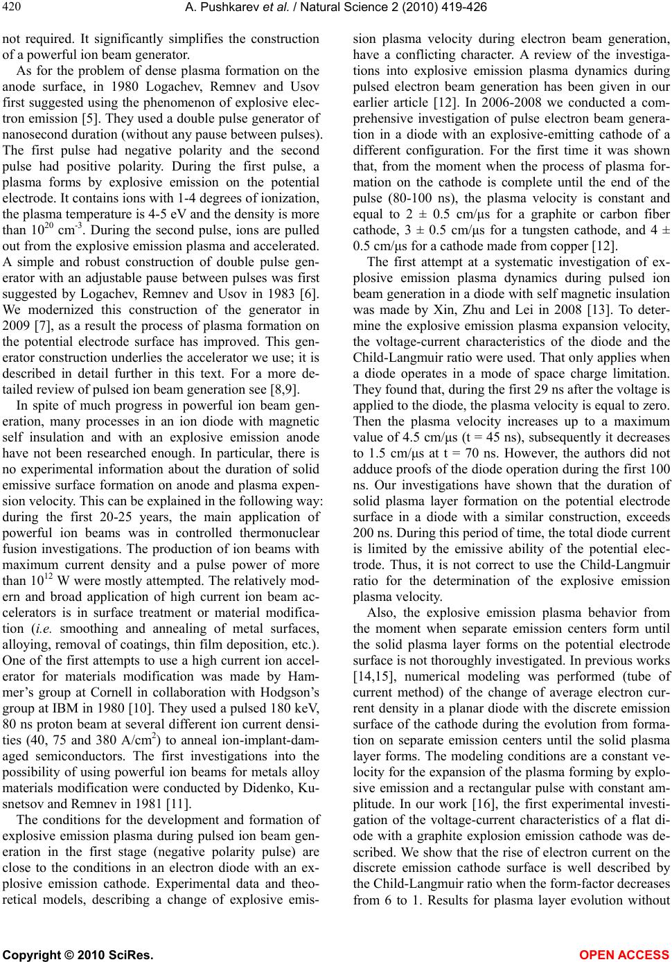 A. Pushkarev et al. / Natural Science 2 (2010) 419-426 Copyright © 2010 SciRes. OPEN ACCESS 420 not required. It significantly simplifies the construction of a powerful ion beam generator. As for the problem of dense plasma formation on the anode surface, in 1980 Logachev, Remnev and Usov first suggested using the phenomenon of explosive elec- tron emission [5]. They used a double pulse generator of nanosecond duration (without any pause between pulses). The first pulse had negative polarity and the second pulse had positive polarity. During the first pulse, a plasma forms by explosive emission on the potential electrode. It contains ions with 1-4 degrees of ionization, the plasma temperature is 4-5 eV and the density is more than 1020 cm-3. During the second pulse, ions are pulled out from the explosive emission plasma and accelerated. A simple and robust construction of double pulse gen- erator with an adjustable pause between pulses was first suggested by Logachev, Remnev and Usov in 1983 [6]. We modernized this construction of the generator in 2009 [7], as a result the process of plasma formation on the potential electrode surface has improved. This gen- erator construction underlies the accelerator we use; it is described in detail further in this text. For a more de- tailed review of pulsed ion beam generation see [8,9]. In spite of much progress in powerful ion beam gen- eration, many processes in an ion diode with magnetic self insulation and with an explosive emission anode have not been researched enough. In particular, there is no experimental information about the duration of solid emissive surface formation on anode and plasma expen- sion velocity. This can be explained in the following way: during the first 20-25 years, the main application of powerful ion beams was in controlled thermonuclear fusion investigations. The production of ion beams with maximum current density and a pulse power of more than 1012 W were mostly attempted. The relatively mod- ern and broad application of high current ion beam ac- celerators is in surface treatment or material modifica- tion (i.e. smoothing and annealing of metal surfaces, alloying, removal of coatings, thin film deposition, etc.). One of the first attempts to use a high current ion accel- erator for materials modification was made by Ham- mer’s group at Cornell in collaboration with Hodgson’s group at IBM in 1980 [10]. They used a pulsed 180 keV, 80 ns proton beam at several different ion current densi- ties (40, 75 and 380 A/cm2) to anneal ion-implant-dam- aged semiconductors. The first investigations into the possibility of using powerful ion beams for metals alloy materials modification were conducted by Didenko, Ku- snetsov and Remnev in 1981 [11]. The conditions for the development and formation of explosive emission plasma during pulsed ion beam gen- eration in the first stage (negative polarity pulse) are close to the conditions in an electron diode with an ex- plosive emission cathode. Experimental data and theo- retical models, describing a change of explosive emis- sion plasma velocity during electron beam generation, have a conflicting character. A review of the investiga- tions into explosive emission plasma dynamics during pulsed electron beam generation has been given in our earlier article [12]. In 2006-2008 we conducted a com- prehensive investigation of pulse electron beam genera- tion in a diode with an explosive-emitting cathode of a different configuration. For the first time it was shown that, from the moment when the process of plasma for- mation on the cathode is complete until the end of the pulse (80-100 ns), the plasma velocity is constant and equal to 2 ± 0.5 cm/μs for a graphite or carbon fiber cathode, 3 ± 0.5 cm/μs for a tungsten cathode, and 4 ± 0.5 cm/μs for a cathode made from copper [12]. The first attempt at a systematic investigation of ex- plosive emission plasma dynamics during pulsed ion beam generation in a diode with self magnetic insulation was made by Xin, Zhu and Lei in 2008 [13]. To deter- mine the explosive emission plasma expansion velocity, the voltage-current characteristics of the diode and the Child-Langmuir ratio were used. That only applies when a diode operates in a mode of space charge limitation. They found that, during the first 29 ns after the voltage is applied to the diode, the plasma velocity is equal to zero. Then the plasma velocity increases up to a maximum value of 4.5 cm/μs (t = 45 ns), subsequently it decreases to 1.5 cm/μs at t = 70 ns. However, the authors did not adduce proofs of the diode operation during the first 100 ns. Our investigations have shown that the duration of solid plasma layer formation on the potential electrode surface in a diode with a similar construction, exceeds 200 ns. During this period of time, the total diode current is limited by the emissive ability of the potential elec- trode. Thus, it is not correct to use the Child-Langmuir ratio for the determination of the explosive emission plasma velocity. Also, the explosive emission plasma behavior from the moment when separate emission centers form until the solid plasma layer forms on the potential electrode surface is not thoroughly investigated. In previous works [14,15], numerical modeling was performed (tube of current method) of the change of average electron cur- rent density in a planar diode with the discrete emission surface of the cathode during the evolution from forma- tion on separate emission centers until the solid plasma layer forms. The modeling conditions are a constant ve- locity for the expansion of the plasma forming by explo- sive emission and a rectangular pulse with constant am- plitude. In our work [16], the first experimental investi- gation of the voltage-current characteristics of a flat di- ode with a graphite explosion emission cathode was de- scribed. We show that the rise of electron current on the discrete emission cathode surface is well described by the Child-Langmuir ratio when the form-factor decreases from 6 to 1. Results for plasma layer evolution without 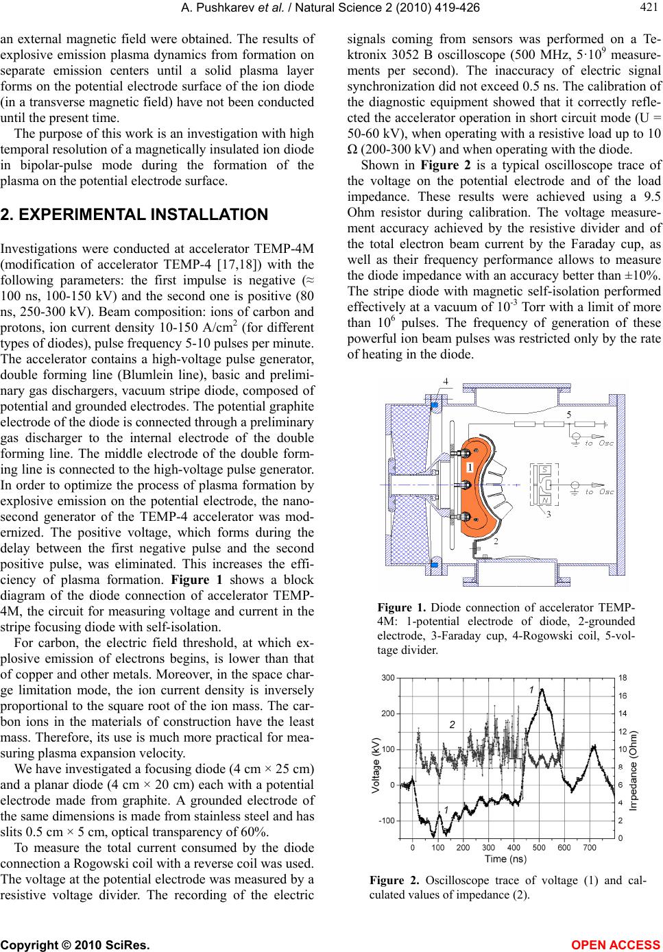 A. Pushkarev et al. / Natural Science 2 (2010) 419-426 Copyright © 2010 SciRes. OPEN ACCESS 421 421 an external magnetic field were obtained. The results of explosive emission plasma dynamics from formation on separate emission centers until a solid plasma layer forms on the potential electrode surface of the ion diode (in a transverse magnetic field) have not been conducted until the present time. The purpose of this work is an investigation with high temporal resolution of a magnetically insulated ion diode in bipolar-pulse mode during the formation of the plasma on the potential electrode surface. 2. EXPERIMENTAL INSTALLATION Investigations were conducted at accelerator TEMP-4M (modification of accelerator TEMP-4 [17,18]) with the following parameters: the first impulse is negative (≈ 100 ns, 100-150 kV) and the second one is positive (80 ns, 250-300 kV). Beam composition: ions of carbon and protons, ion current density 10-150 A/cm2 (for different types of diodes), pulse frequency 5-10 pulses per minute. The accelerator contains a high-voltage pulse generator, double forming line (Blumlein line), basic and prelimi- nary gas dischargers, vacuum stripe diode, composed of potential and grounded electrodes. The potential graphite electrode of the diode is connected through a preliminary gas discharger to the internal electrode of the double forming line. The middle electrode of the double form- ing line is connected to the high-voltage pulse generator. In order to optimize the process of plasma formation by explosive emission on the potential electrode, the nano- second generator of the TEMP-4 accelerator was mod- ernized. The positive voltage, which forms during the delay between the first negative pulse and the second positive pulse, was eliminated. This increases the effi- ciency of plasma formation. Figure 1 shows a block diagram of the diode connection of accelerator TEMP- 4M, the circuit for measuring voltage and current in the stripe focusing diode with self-isolation. For carbon, the electric field threshold, at which ex- plosive emission of electrons begins, is lower than that of copper and other metals. Moreover, in the space char- ge limitation mode, the ion current density is inversely proportional to the square root of the ion mass. The car- bon ions in the materials of construction have the least mass. Therefore, its use is much more practical for mea- suring plasma expansion velocity. We have investigated a focusing diode (4 cm × 25 cm) and a planar diode (4 cm × 20 cm) each with a potential electrode made from graphite. A grounded electrode of the same dimensions is made from stainless steel and has slits 0.5 cm × 5 cm, optical transparency of 60%. To measure the total current consumed by the diode connection a Rogowski coil with a reverse coil was used. The voltage at the potential electrode was measured by a resistive voltage divider. The recording of the electric signals coming from sensors was performed on a Te- ktronix 3052 B oscilloscope (500 MHz, 5·109 measure- ments per second). The inaccuracy of electric signal synchronization did not exceed 0.5 ns. The calibration of the diagnostic equipment showed that it correctly refle- cted the accelerator operation in short circuit mode (U = 50-60 kV), when operating with a resistive load up to 10 Ω (200-300 kV) and when operating with the diode. Shown in Figure 2 is a typical oscilloscope trace of the voltage on the potential electrode and of the load impedance. These results were achieved using a 9.5 Ohm resistor during calibration. The voltage measure- ment accuracy achieved by the resistive divider and of the total electron beam current by the Faraday cup, as well as their frequency performance allows to measure the diode impedance with an accuracy better than ±10%. The stripe diode with magnetic self-isolation performed effectively at a vacuum of 10-3 Torr with a limit of more than 106 pulses. The frequency of generation of these powerful ion beam pulses was restricted only by the rate of heating in the diode. Figure 1. Diode connection of accelerator TEMP- 4M: 1-potential electrode of diode, 2-grounded electrode, 3-Faraday cup, 4-Rogowski coil, 5-vol- tage divider. Figure 2. Oscilloscope trace of voltage (1) and cal- culated values of impedance (2).  A. Pushkarev et al. / Natural Science 2 (2010) 419-426 Copyright © 2010 SciRes. OPEN ACCESS 422 3. BASIC CALCULATION EQUATIONS An analysis of plasma behavior in the anode-cathode gap was performed based on the current-voltage characteris- tics of the diode. The electron and ion current densities flowing through the diode in the mode restricted by space charge are determined by the following expres- sions [1]: Electron current: 2 0 3/2 6 2 0 3/2 e 0 e102.33 9 24ε d U d U m e J (1) Ion current: 2 0 2/3 0 9 24 d U m z J i i ion (2) where U is the voltage applied to the diode; d0 is the anode-cathode gap, me is electron mass; mi is ionic mass; zi is ionic charge. Taking into account the reduction of anode-cathode gap due to expansion of plasma from the emissive sur- face of the potential electrode, the electron current den- sity is equal to: 2 0 3/2 6 e)( 102.33)( vtd U tJ (3) where v is plasma expansion velocity. If the diode operates in the mode of space charge limitation, then from correlation (3), we obtain the cath- ode plasma expansion speed as: 63/2 0 0 e 2.33 10 1 () SU vt d tI (4) where S0 is the surface area of potential electrode (cath- ode during negative pulsed) of diode. This correlation is used further down in the calculation of plasma expansion speed. The speed at which the cathode plasma spreads can be correctly calculated from the current-voltage characteris- tics of the diode only under operating conditions corre- sponding to the mode of space charge limitation. The mode operation of the diode can easily be determined by comparing the experimental and calculated values of diode impedance. Their coincidence corresponds to the diode current being limited by space charge. In the initial period (discrete emission surface mode) and in the satu- ration mode, the diode current is limited by the electron emission from cathode. This is why the experimental values of impedance will be larger than the calculated ones. It is evident from Eq.1 and Eq.2, that the ion cur- rent amounts to only a small part of the total current through the diode, therefore the impedance of the diode can be calculated from the following: 1/26 0 2 0 e0 calc 102.33 )( US tvd JS U R (5) 4. DISCRETE EMISSIVE SURFACE MODE Operation of the magnetic self-isolation diode at the first (negative) pulse and during the pause between pulses is analogous to the operation mode of a planar diode with explosive emission cathode at electron beam generation. In Figure 3, a typical oscilloscope trace of the voltage on the potential graphite electrode and calculated values of the diode impedance are displayed. Two modes of operation can be singled out [12,19]. From the application of voltage until the formation of a solid plasma surface at the potential electrode (discrete emissive surface mode, 0 < t < 250 ns in Figure 3), the diode current is limited by the emissive ability of the cathode. After covering the potential electrode surface with plasma, the total diode current is limited only by the vacuum electron charge in the anode-cathode gap (250 ns < t < 600 ns in Figure 3). Reduction of impedance of the diode in discrete emis- sive surface mode is connected with two processes. They are the increase of emissive surface on the graphite elec- trode and the reduction of anode-cathode gap through movement of the explosive emission plasma towards the grounded electrode (Eq.5). The origin of the reduction in diode impedance in space charge limitation mode is the reduction of anode-cathode gap only. The diode changes to the space charge limitation mode after formation of the solid emissive layer on the cathode surface. Let us assume that: 1) the electron cur- rent is limited by the space charge in the inter-electrode gap from the first moment of voltage application to the diode, and 2) electron beam current growth until saturation Figure 3. Oscilloscope trace of voltage (1) and im- pedance value (2-experiment, 3-calculation) of stripe fo- cusing diode with self-isolation, anode-cathode gap 8 mm.  A. Pushkarev et al. / Natural Science 2 (2010) 419-426 Copyright © 2010 SciRes. OPEN ACCESS 423 423 is determined by an increase in the surface of discrete emitting centers from zero to the total geometric area of the cathode. This approach has been successfully veri- fied [14,15] by modelling the variation of the average electron beam current in a planar diode with a discrete emitting surface. Using Eq.3 the total electron current of the diode is: 2 0 3/2 6 e)( )( 102.33 tvd tSU I where S(t) - total area of plasma emissive surface on the cathode. In modelling the law of variation of the area of a dis- crete emitting surface, we use the following assumptions [16]: 1) the emitting centers are equidistant from each other and form a uniform cellular structure on the cath- ode surface; 2) the emitting centers are formed simulta- neously and their number remains the same during the entire period of electron beam generation. Thus, the total emitting area on the cathode is: )sin(3π)()( 2 1ααtvNtS where N - number of emitting centers; v1 - speed of ex- pansion of the explosive emission plasma across the gap, α = 2arcos(b/v1·t), b - distance between adjoining emit- ting centers. The total number of emitting centers can be estimated as the ratio of the cathode area to the area of a hexagonal unit cell (0.865b2). Consequently, the total electron cur- rent emitted by the discrete emissive surface is: 3/2 2 0 2 0 2 1 6 calc )( )sin3(π)(102.7 U tvdb Sααtv I (6) Figure 4 shows the current changing during plasma formation by explosive emission on the potential elec- trode of the focusing diode. Experimental data are com- pared with calculated data based on the assumption that emitting centers form and expand (Eq.6, v1 = 2 cm/μs, b = 11 mm); within the presence of a solid plasma surface when the voltage is applied (Eq.3). Calculations were made of the total electron current of the diode with dis- crete emissive surface based on the assumption that the speed of expansion of the explosive emission plasma across the anode-cathode gap is equal to the speed of expansion of the graphite plasma without any magnetic field. The minimum distance between individual emit- ting centers was calculated from the electric field screening around the center [20]: cm,500 3/41/2 10 UIdr The radius of screening, r, is equal to 5-6 mm if the electron current from one emitting center I1 = 90 A and the average voltage applied to the diode, during emitting center formation is 100-120 kV (see Figure 3). Measurements taken of the spatial distribution of en- ergy density in the electron beam formed by the diode during the first pulse confirm the existence of a periodic structure in the emitting surface on the potential elec- trode. The distribution of energy density of electrons over the cross section was measured by using a special do- simetric film. The method of measurement is described in detail in our reference [21]. Figure 5 illustrates the change of electron beam energy density across the diode. The dosimetric film was placed in the outside of the grounded electrode. To protect it from the effects of the ion beam, the films were covered with aluminum foil with a thickness of 15 microns. Due to the screening of the dosimetric film by slits (0.5 cm × 5 cm) on the grounded electrode, the density reduces to zero at x = 10 and 70 mm. During the process in which the discrete emissive surface spreads from separate emitting centers to a solid plasma layer that covers the cathode, a form factor must be incorporated in Eq.6 [19]. This form factor accounts for the distortion of the electric field strength near emitting Figure 4. The diode current changing during plasma formation by explosive emission: (1) experimental data, and calculation for (2) solid and (3) discrete plasma surface on the cathode. Figure 5. Distribution of energy density in the elec- tron beam (cross section).  A. Pushkarev et al. / Natural Science 2 (2010) 419-426 Copyright © 2010 SciRes. OPEN ACCESS 424 centers [20]. The dependence of planar diode current with a discrete emissive cathode is: FU tvdb Stv Icalc 2/3 2 0 2 0 2 1 6 )( )sin(3)(107.2 It has been demonstrated [22,23] that the current- voltage characteristic of a planar diode with flat elec- trodes (U = 20-40 kV) and a single emitter arising at an artificial micro-protrusion on the cathode surface (d = 0.3-1 mm) in the initial stage of emitter evolution (v·t < d/3) is well described (to within 10%) by the following relation: 2 0 3/26 1044.4 d tv UI Note that this expression is obtained from correlation (1) for a cathode with an emitting area of π(v·t)2 and F = 6. Figure 6 shows the ratio of experimental values of diode current divided by calculated values based on the correlation (6). This ratio reflects the change in form factor during explosive emission plasma formation. There are 4 typi- cal ranges for the form factor. During the initial period of time (t < 80 ns) the value of the form factor exceeds 6, which fits with an increase in the number of emitting centers and a simultaneous increase in their sizes. Dur- ing the time that the ratio of distance between adjacent emitting centers to their radius decreases from 7 to 5 (80 < t < 100 ns, see Figure 6) the formation of additional emitting centers is suppressed by screening effects. The value of the form factor is constant (within the meas- urement accuracy) and is equal to 6. Furthermore, with the size of the emitting center increasing as neighboring centers overlap, the value of F decreases to 1. Thus, a continuous emission surface forms on the graphite cath- ode to generate the second pulse, F = 1. Previous research has shown that the duration of solid emissive layer formation on the cathode surface (only when congruent with the duration of the pulse edge) depends on the area and material of the cathode [16]. Figure 7 gives a comparison of the duration of explosive emission plasma formation on the graphite cathode sur- face of an electron diode (400 kV, 10 kA, 80 ns). This was done with both 45 and 60 mm diameter cathodes. The values of the duration of solid emissive surface formation on the potential graphite electrode of the ion diode (flat and focusing geometries) in the self-magnetic insulation mode (first pulse) are illustrated in Figure 7. It was shown that, in the discrete emissive surface mode, the influence of the magnetic field on the dynamics of the cathode plasma in a magnetically insu- lated diode is negligible. 5. SPACE СHARGE LIMITATION MODE After covering the potential electrode surface with plasma, the total diode current is limited only by the electron charge in the anode-cathode gap (250 ns < t < 600 ns in Figure 3). Experimental values of the diode impedance are well described by correlation (5). Figure 8 shows the values of cathode plasma expansion speed calculated from Eq.4. Through these experiments we have found that the rate of expansion of a graphite plasma (across the anode- cathode gap) in a magnetically insulated diode is sig- nificantly lower than the plasma rate of expansion in an electron diode with graphite explosive emission cathode [12]. This indicates the significant influence of the mag- netic field in the gap on the expansion dynamics of an explosive emission plasma. In the generation of power- ful ion beams, the reduction of the rate of expansion of the explosive emission plasma is a useful effect which decreases the possibility of the anode-cathode gap being bridged by the plasma. Figure 6. Oscilloscope trace of voltage (1) and form-factor for the formation of the plasma surface on the cathode (2). Figure 7. Dependence of the duration of solid emis- sive surface formation on graphite cathode surface area.  A. Pushkarev et al. / Natural Science 2 (2010) 419-426 Copyright © 2010 SciRes. OPEN ACCESS 425 425 Figure 8. Change of explosive emission plasma speed during beam generation in electron diode with graphite cathode (1) and in planar ion (2) and focusing ion (3) diodes with graphite potential electrode. 6. DISCUSSION OF EXPERIMENTAL RESULTS To provide magnetic insulation to the electrons in the di- ode, the grounded electrode is connected to a camera only from one side. Electrons, which compose the major part of charge carriers in the diode, generate a magnetic field as they move through the electrode (or along the surface). The magnetic field vector is perpendicular to the elec- tric field vector in the anode-cathode gap. Figure 9 shows the change in magnetic induction in the diode during the formation of the explosive-emission plasma and the generation of the ion beam (according to the Biot-Savart law). The calculation of magnetic field using the ratio, based on diode geometry [13], gives results in close agreement. We consider an electron, emitted from the explosive emission plasma on the potential electrode at the start of the first pulse. Under the influence of the electric field, it is accelerated towards the grounded electrode. In crossed electric and magnetic fields under the influence of the Lorentz force, the electron begins to change its direction of motion from a transverse one to a longitudinal one, along the grounded electrode. The Lorentz force does no work and does not change the energy (or velocity) of the electron, but changes only the direction of motion. Elec- tron motion in crossed electric and magnetic fields can be represented as a rotation over the cyclotron circum- ference with the center of the circumference drifting in the direction perpendicular to vectors E and B. The drift velocity is equal to the ratio of electric field strength to magnetic induction. At the first pulse, the electrons are emitted from the plasma surface on the potential electrode and move to- wards the grounded electrode, which is a current-car- rying conductor. The magnetic induction in the anode- cathode gap increases towards the grounded electrode. When the electron approaches the distance to the groun- ded electrode, at which the magnetic induction exceeds Вcr, the electron fails to reach its surface because it is in cycloidal motion in the diode gap along the grounded electrode. However, the electron motion in vacuum in the diode gap comprises the current of the grounded electrode and generates a self-magnetic field. The change of critical magnetic induction during for- mation of the plasma on the cathode by explosive emis- sion is shown in Figure 9. It is obvious that during the first 200-300 ns (discrete emissive surface mode) the magnetic field induction in the whole anode-cathode gap exceeds Вcr. This points to the fact that at the first pulse, electrons move into the anode-cathode gap near the potential electrode surface. It is evident that the influence of the magnetic field on the value of electron current (magnetic cut-off) is sig- nificant when the duration of electron drift in crossed magnetic and electric fields is comparable to the dura- tion of the voltage pulse applied to the diode. The aver- age drift velocity is equal to 12 cm/ns, and the elec- trons reach the end of the diode (electrode length of 25 cm) within 2 ns. Therefore the effect of magnetic insula- tion at the first pulse is insignificant. It is important to note that, at the first pulse, only a small portion of elec- trons reach the surface of the grounded electrode, which restricts the process of plasma creation near the anode surface. 7. CONCLUSIONS An analysis of the pulsed ion diode with a passive anode in the double-pulse mode, with matching of the diode impedance to the output resistance of the nanosecond generator has shown that the effect of magnetic self- isolation is significant only during ion beam generation (second pulse). In the initial period, at the stage of forming explosive centres and developing the potential electrode emission surface of the diode, the plasma dy- namics are similar to the processes in the electronic diode Figure 9. (1) the change of the accelerating voltage; (2) the magnetic induction close to the potential electrode; (3) critical magnetic induction.  A. Pushkarev et al. / Natural Science 2 (2010) 419-426 Copyright © 2010 SciRes. OPEN ACCESS 426 of a pulsed electron accelerator. After the solid plasma forms on the surface of the passive anode, the effect of magnetic insulation manifests itself only in a reduction of the rate of explosive emission plasma expansion across the gap. The value of electron current amounts to more than 90% of the total diode current. It is well de- scribed by the model of space charge limitation. The electron drift duration in the crossed magnetic and elec- tric fields during plasma formation in the passive anode does not exceed a few nanoseconds, and the height of the Trochoid of drift motion is close to the value of the anode-cathode gap. The results of our investigations show that the experi- mental current-voltage characteristics of a magnetically insulated ion diode with a graphite explosive emission cathode in the initial stage (featuring a discrete emitting surface) is satisfactorily described by a modified Child- Langmuir formula, assuming that all discrete emitters are formed simultaneously, their number is constant, and the emitter radius increases at a constant rate. In the ini- tial period of time, when the emitter radius is much smaller than the distance between adjacent emitters, the form factor in the modified Child-Langmuir formula cor- responds to the experimental value F = 6, obtained for a diode with a single emitting center. As the emitter area increases, the form factor decreases from F = 6 to 1, which corresponds to the current-voltage characteristic of a planar diode with a continuous emitting surface on the graphite cathode. 8. ACKNOWLEDGMENTS This work was supported by the Russian Foundation for Basic Re- search under project No. 08-08-12086. REFERENCES [1] Langmuir, I. (1913) The effect of space charge and residual gases on thermionic currents in high vacuum. Physical Review, 2(6), 450-486. [2] Sudan, R.N. and Lovelace, R.V. (1973) Generation of intense ion beams in pulsed diodes. Physical Review Letters, 31(19), 1174-1177. [3] Dreike, P., Eichenberger, C., Humphries, S. and Sudan, R. (1976) Production of intense proton fluxes in a magneti- cally insulated diode. Journal of Applied Physics, 47(1), 85-88. [4] Humphries, S. (1977) Self magnetic insulation of pulsed ion diodes. Plasma Physics, 19(5), 399-406. [5] Logachev, E.I., Remnev, G.E. and Usov, Y.P. (1980) Ion acceleration from explosion-emissive plasma. Techni- cal Physics Letters, 6(22), 1404-1406. [6] Logachev, E.I., Remnev, G.E. and Usov, Y.P. (1983) Generator of nanosecond pulsed. Soviet Patent SU 852149A. [7] Pushkarev, A.I., Tarbokov, V.A., Sazonov, R.V. and Isakov, I.F. (2009) Pulsed ion generator. Russian Patent RU 86374 U1. [8] Bystrickii, V.M. and Didenko, A.N. (1984) High-power ion beams. Energoatomizdat, Moscow. [9] Gordon, A.M. (2006) Ph.D. Dessertation, Tomsk Poly- technic University, Tomsk. [10] Hodgson, R.T., Baglin, J.E.E., Pal, R., Neri, J.M. and Hammer, D.A. (1980) Ion beam annealing of semicon- ductors. Applied Physics Letters, 37(2), 187-189. [11] Didenko, A.N., Kusnetsov, B.I. and Remnev, G.E. (1981) Proceedings of National Conference Application of Electron and Ion Technology in National Economy, Tbilisi. [12] Pushkarev, A.I. and Sazonov, R.V. (2009) Research of cathode plasma speed in planar diode with explosive emission cathode. IEEE Transactions on Plasma Science, 37(10), 1901-1907. [13] Xin, J.P., Zhu, X.P. and Lei, M.K. (2008) Initial plasma of a magnetically insulated ion diode in bipolar-pulse mode. Physics Plasmas, 15(12), 123101-123108. [14] Belomyttsev, S.Y., Korovin, S.D. and Pegel, I.V. (1999) Current in a high-current planar diode with a discrete emitting surface. Technical Physics, 44(6), 695-699. [15] Djogo, G. and Gross, J.D. (1997) Circuit modeling of a vacuum gap during breakdown. IEEE Transactions on Plasma Science, 25(4), 617-624. [16] Pushkarev, A.I. and Sazonov, R.V. (2008) A planar diode operating in the regime of limited electron emission. Technical Physics Letters, 34(4), 292-295. [17] Remnev, G.E., Isakov, I.F., Opekounov, M.S., Kotlya- revsky, G.I., Matvienko, V.M., et al. (1997) High-power ion sources for industrial application. Surface and Coatings Technology, 96(1), 103-109. [18] Remnev, G.E., Isakov, I.F., Opekounov, M.S., Matvienko, V.M., Pushkarev, A.I., et al. (1999) High Intensity pulsed ion beam sources and their industrial applications. Surface and Coatings Technology, 114(2-3), 206-212. [19] Pushkarev, A.I. (2008) Perveance of a planar diode with a multipoint cathode. Technical Physics, 53(3), 363-367. [20] Mesyats, G.A. (2000) Actons in vacuum discharge: Breakdown, the spark, and the ark. Nauka, Moscow. [21] Pushkarev, A.I. and Sazonov, R.V. (2007) Research of high-current pulsed electron beam energy distribution in depth of sheet of water. Bulletin of Tomsk Polytechnic University, 311(2), 47-50. [22] Mesyats, G.A. (2004) Pulsed power and electronics. Nauka, Moscow. [23] Shubin, A.F. and Yurike, Y.Y. (1975) Current rise in the initial stages of vacuum breakdown between plane ele- ctrodes with slowly increasing voltage. Russion Physics Journal, 18(6), 870-872. |