Paper Menu >>
Journal Menu >>
 Int. J. Communications, Network and System Sciences, 2010, 3, 434-440 doi:10.4236/ijcns.2010.35057 Published Online May 2010 (http://www.SciRP.org/journal/ijcns/) Copyright © 2010 SciRes. IJCNS Measurements of Balun and Gap Effects in a Dipole Antenna Constantinos Votis1, Vasilis Christofilakis1,2, Panos Kostarakis1 1Physics Department, University of Ioannina, Panepistimioupolis, Ioannina, Greece 2Siemens Enterprise Communications, Enterprise Products Development, Athens, Greece E-mail: kvotis@grads.uoi.gr, basilios.christofilakis@siemens-enterprise.com, kostarakis@uoi.gr Received February 12, 2010; revised March 15, 2010; accepted April 18, 2010 Abstract In the present paper, design and analysis of a 2.4 GHz printed dipole antenna for wireless communication applications are presented. Measurements on return loss and radiation pattern of this antenna configuration are included in this investigation. The printed dipole is combined with the feeding structure of a microstrip via-hole balun and is fabricated on an FR-4 printed-circuit-board substrate. Two inevitable discontinuities are introduced by this antenna architecture in the form of right-angle bends in the microstrip feed line and in the dipole’s gap, respectively. The impact of mitering these bends in the reflection coefficient, resonance bandwidth and radiation pattern of antenna has been investigated by means of simulation and experiment. Keywords: Printed Dipole, Integrated Balun, S-Parameters, Radiation Pattern 1. Introduction The microstrip antenna architecture, in general, offers inherent narrow bandwidth and quite low gain. These limitations do not provide wide usage of these antennas in wireless applications systems. Besides, the evolution of wireless communications leads to more compact and small equipment that demanding antennas with smaller size and profile. Hence, the scientific community has started to investigate methods to improve this antenna architecture and provide better quality of services on wireless communication systems. In this way, many re- search activities were based on the printed dipole an- tenna because it has low profile, simple structure and omnidirectional radiation pattern. In order to develop this antenna configuration a printed dipole antenna with inte- grated balun and microstrip line as feeding structure was proposed [1-3]. Based on these considerations, we design and fabricate a 2.4-GHz printed dipole antenna with in- tegrated microstrip balun. This antenna design offers all the advantages of printed circuits and the corresponding geometry characteristics have been in detail studied and investigated [4-5]. In order to improve the bandwidth and the gain of this architecture we study and investigate the impact on variations of the l and w geometrical parame- ters on antenna performance. The first corresponds to the right angle bend in the microstrip balun and the second affects the dipole’s arms. Details of the structure and design process are presented in the next section (Section 2). The corresponding simulated and measured results are presented and discussed in Section 3. The paper con- cludes in Section 4. 2. Design Process and Structure The geometry and design parameters of the 2.4 GHz prin- ted dipole antenna are drawn in Figure 1. It is a modified antenna design that was introduced by the corresponding literature [1-4]. This printed dipole antenna was etched on Fr4 sub- strate with thickness h = 1.5 mm and permittivity εr = 4.4. The ground plane of the microstrip line and the di- pole strips were printed at the bottom layer. A microstrip via-hole balun acts as an unbalance-to-balance trans- former from the coaxial line to the printed dipole strip. The lengths of the dipole—arm strips and the microstrip balun are approximately a quarter—wavelength [4-6]. Based on matching techniques theory, the integrated balun affects the current flow at each dipole—arm, be- cause of cancellation of the current flow to ground on the outside part of the outer conductor in corresponding co- axial line. In fact, the balun configuration ensures that the currents which flow the dipole arms become quite identical without eliminating the radiation efficiency [6]. The structure parameters of the proposed dipole for 2.4 GHz frequency point are listed as follows: 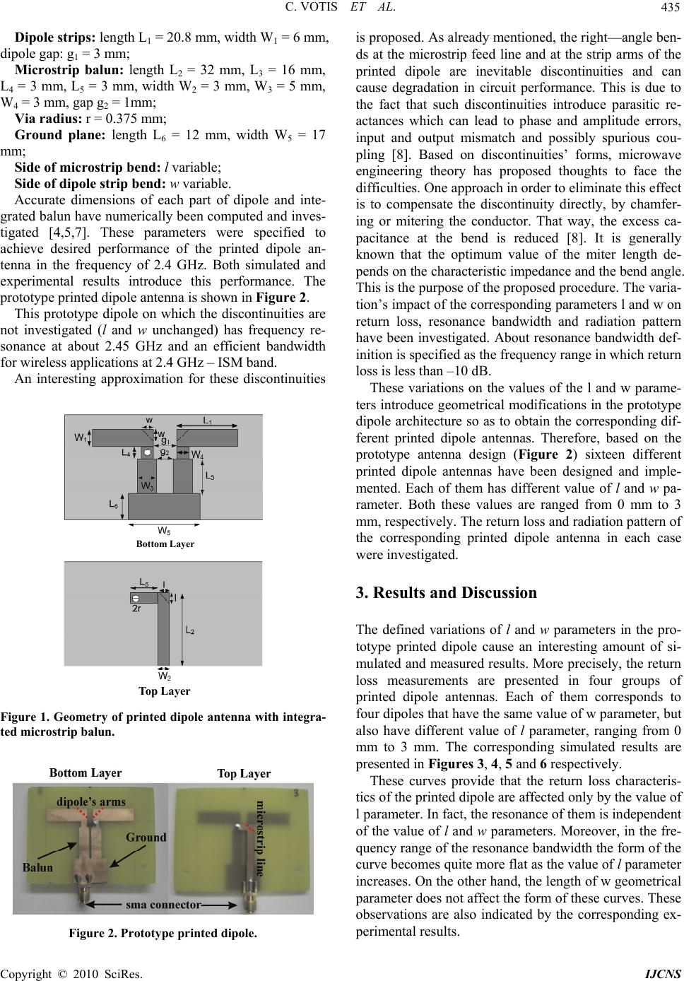 C. VOTIS ET AL. Copyright © 2010 SciRes. IJCNS 435 Dipole strips: length L1 = 20.8 mm, width W1 = 6 mm, dipole gap: g1 = 3 mm; Microstrip balun: length L2 = 32 mm, L3 = 16 mm, L4 = 3 mm, L5 = 3 mm, width W2 = 3 mm, W3 = 5 mm, W4 = 3 mm, gap g2 = 1mm; Via radius: r = 0.375 mm; Ground plane: length L6 = 12 mm, width W5 = 17 mm; Side of microstrip bend: l variable; Side of dipole strip bend: w variable. Accurate dimensions of each part of dipole and inte- grated balun have numerically been computed and inves- tigated [4,5,7]. These parameters were specified to achieve desired performance of the printed dipole an- tenna in the frequency of 2.4 GHz. Both simulated and experimental results introduce this performance. The prototype printed dipole antenna is shown in Figure 2. This prototype dipole on which the discontinuities are not investigated (l and w unchanged) has frequency re- sonance at about 2.45 GHz and an efficient bandwidth for wireless applications at 2.4 GHz – ISM band. An interesting approximation for these discontinuities Bottom La y er Top Layer Figure 1. Geometry of printed dipole antenna with integra- ted microstrip balun. Figure 2. Prototype printed dipole. is proposed. As already mentioned, the right—angle ben- ds at the microstrip feed line and at the strip arms of the printed dipole are inevitable discontinuities and can cause degradation in circuit performance. This is due to the fact that such discontinuities introduce parasitic re- actances which can lead to phase and amplitude errors, input and output mismatch and possibly spurious cou- pling [8]. Based on discontinuities’ forms, microwave engineering theory has proposed thoughts to face the difficulties. One approach in order to eliminate this effect is to compensate the discontinuity directly, by chamfer- ing or mitering the conductor. That way, the excess ca- pacitance at the bend is reduced [8]. It is generally known that the optimum value of the miter length de- pends on the characteristic impedance and the bend angle. This is the purpose of the proposed procedure. The varia- tion’s impact of the corresponding parameters l and w on return loss, resonance bandwidth and radiation pattern have been investigated. About resonance bandwidth def- inition is specified as the frequency range in which return loss is less than –10 dB. These variations on the values of the l and w parame- ters introduce geometrical modifications in the prototype dipole architecture so as to obtain the corresponding dif- ferent printed dipole antennas. Therefore, based on the prototype antenna design (Figure 2) sixteen different printed dipole antennas have been designed and imple- mented. Each of them has different value of l and w pa- rameter. Both these values are ranged from 0 mm to 3 mm, respectively. The return loss and radiation pattern of the corresponding printed dipole antenna in each case were investigated. 3. Results and Discussion The defined variations of l and w parameters in the pro- totype printed dipole cause an interesting amount of si- mulated and measured results. More precisely, the return loss measurements are presented in four groups of printed dipole antennas. Each of them corresponds to four dipoles that have the same value of w parameter, but also have different value of l parameter, ranging from 0 mm to 3 mm. The corresponding simulated results are presented in Figures 3, 4, 5 and 6 respectively. These curves provide that the return loss characteris- tics of the printed dipole are affected only by the value of l parameter. In fact, the resonance of them is independent of the value of l and w parameters. Moreover, in the fre- quency range of the resonance bandwidth the form of the curve becomes quite more flat as the value of l parameter increases. On the other hand, the length of w geometrical parameter does not affect the form of these curves. These observations are also indicated by the corresponding ex- perimental results. 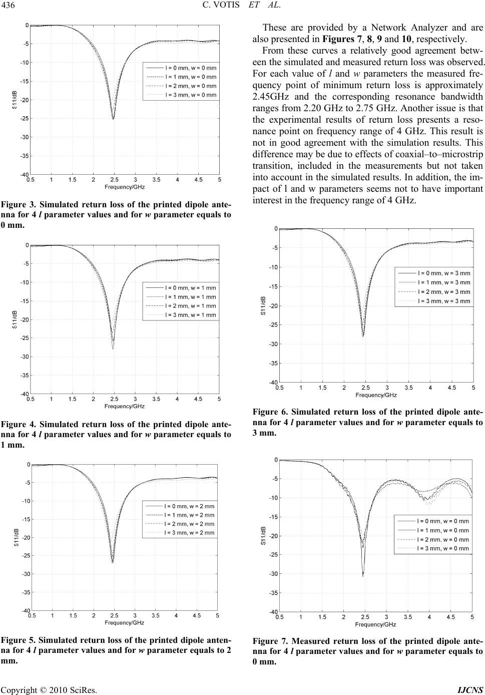 C. VOTIS ET AL. Copyright © 2010 SciRes. IJCNS 436 Figure 3. Simulated return loss of the printed dipole ante- nna for 4 l parameter values and for w parameter equals to 0 mm. Figure 4. Simulated return loss of the printed dipole ante- nna for 4 l parameter values and for w parameter equals to 1 mm. Figure 5. Simulated return loss of the printed dipole anten- na for 4 l parameter values and for w parameter equals to 2 mm. These are provided by a Network Analyzer and are also presented in Figures 7, 8, 9 and 10, respectively. From these curves a relatively good agreement betw- een the simulated and measured return loss was observed. For each value of l and w parameters the measured fre- quency point of minimum return loss is approximately 2.45GHz and the corresponding resonance bandwidth ranges from 2.20 GHz to 2.75 GHz. Another issue is that the experimental results of return loss presents a reso- nance point on frequency range of 4 GHz. This result is not in good agreement with the simulation results. This difference may be due to effects of coaxial–to–microstrip transition, included in the measurements but not taken into account in the simulated results. In addition, the im- pact of l and w parameters seems not to have important interest in the frequency range of 4 GHz. Figure 6. Simulated return loss of the printed dipole ante- nna for 4 l parameter values and for w parameter equals to 3 mm. Figure 7. Measured return loss of the printed dipole ante- nna for 4 l parameter values and for w parameter equals to 0 mm. 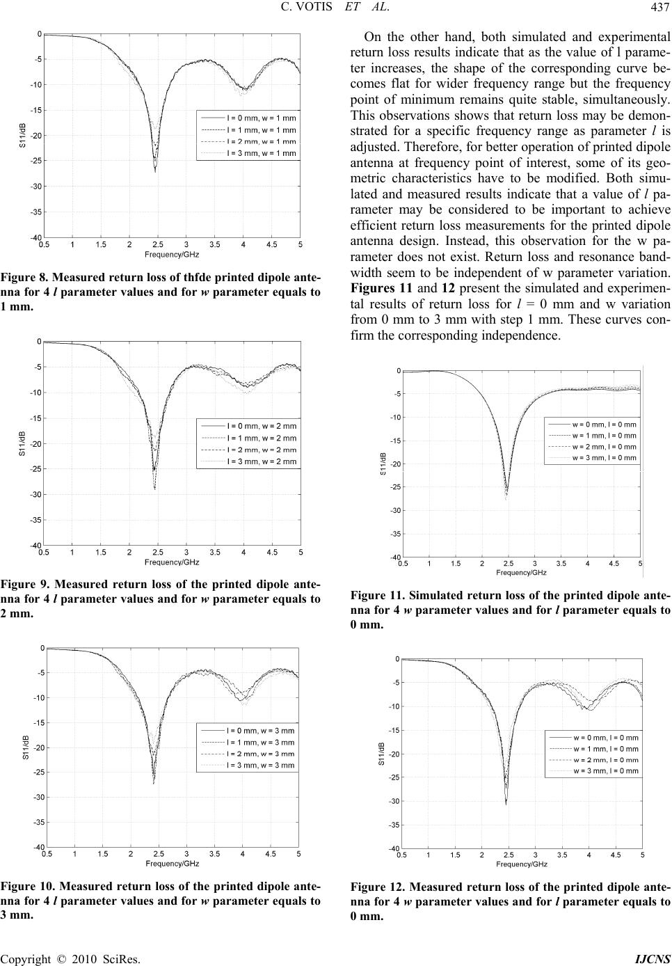 C. VOTIS ET AL. Copyright © 2010 SciRes. IJCNS 437 Figure 8. Measured return loss of thfde printed dipole ante- nna for 4 l parameter values and for w parameter equals to 1 mm. Figure 9. Measured return loss of the printed dipole ante- nna for 4 l parameter values and for w parameter equals to 2 mm. Figure 10. Measured return loss of the printed dipole ante- nna for 4 l parameter values and for w parameter equals to 3 mm. On the other hand, both simulated and experimental return loss results indicate that as the value of l parame- ter increases, the shape of the corresponding curve be- comes flat for wider frequency range but the frequency point of minimum remains quite stable, simultaneously. This observations shows that return loss may be demon- strated for a specific frequency range as parameter l is adjusted. Therefore, for better operation of printed dipole antenna at frequency point of interest, some of its geo- metric characteristics have to be modified. Both simu- lated and measured results indicate that a value of l pa- rameter may be considered to be important to achieve efficient return loss measurements for the printed dipole antenna design. Instead, this observation for the w pa- rameter does not exist. Return loss and resonance band- width seem to be independent of w parameter variation. Figures 11 and 12 present the simulated and experimen- tal results of return loss for l = 0 mm and w variation from 0 mm to 3 mm with step 1 mm. These curves con- firm the corresponding independence. Figure 11. Simulated return loss of the printed dipole ante- nna for 4 w parameter values and for l parameter equals to 0 mm. Figure 12. Measured return loss of the printed dipole ante- nna for 4 w parameter values and for l parameter equals to 0 mm. 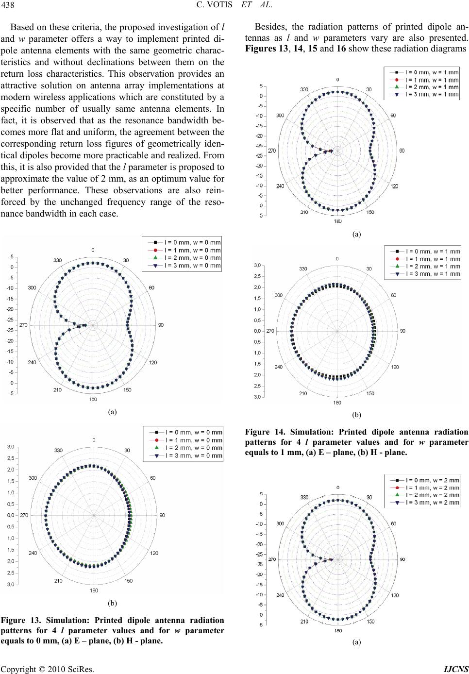 C. VOTIS ET AL. Copyright © 2010 SciRes. IJCNS 438 Based on these criteria, the proposed investigation of l and w parameter offers a way to implement printed di- pole antenna elements with the same geometric charac- teristics and without declinations between them on the return loss characteristics. This observation provides an attractive solution on antenna array implementations at modern wireless applications which are constituted by a specific number of usually same antenna elements. In fact, it is observed that as the resonance bandwidth be- comes more flat and uniform, the agreement between the corresponding return loss figures of geometrically iden- tical dipoles become more practicable and realized. From this, it is also provided that the l parameter is proposed to approximate the value of 2 mm, as an optimum value for better performance. These observations are also rein- forced by the unchanged frequency range of the reso- nance bandwidth in each case. (a) (b) Figure 13. Simulation: Printed dipole antenna radiation patterns for 4 l parameter values and for w parameter equals to 0 mm, (a) E – plane, (b) H - plane. Besides, the radiation patterns of printed dipole an- tennas as l and w parameters vary are also presented. Figures 13, 14, 15 and 16 show these radiation diagrams (a) (b) Figure 14. Simulation: Printed dipole antenna radiation patterns for 4 l parameter values and for w parameter equals to 1 mm, (a) E – plane, (b) H - plane. (a) 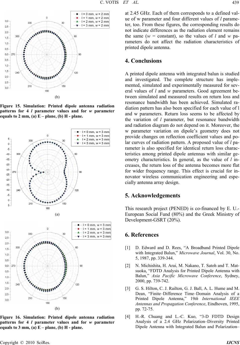 C. VOTIS ET AL. Copyright © 2010 SciRes. IJCNS 439 (b) Figure 15. Simulation: Printed dipole antenna radiation patterns for 4 l parameter values and for w parameter equals to 2 mm, (a) E – plane, (b) H - plane. (a) (b) Figure 16. Simulation: Printed dipole antenna radiation patterns for 4 l parameter values and for w parameter equals to 3 mm, (a) E – plane, (b) H - plane. at 2.45 GHz. Each of them corresponds to a defined val- ue of w parameter and four different values of l parame- ter, too. From these figures, the corresponding results do not indicate differences as the radiation element remains the same (w = constant), so the values of l and w pa- rameters do not affect the radiation characteristics of printed dipole antenna. 4. Conclusions A printed dipole antenna with integrated balun is studied and investigated. The complete structure has imple- mented, simulated and experimentally measured for sev- eral values of l and w parameters. Good agreement be- tween simulated and measured results on return loss and resonance bandwidth has been achieved. Simulated ra- diation pattern has also been specified for each value of l and w parameters. Return loss seems to be affected by the variation of l parameter, but resonance bandwidth and radiation diagram do not depend on it. Moreover, the w parameter variation on dipole’s geometry does not provide changes on reflection coefficient values and po- lar curves of radiation pattern. A proposed value of l pa- rameter is also specified for identical return loss charac- teristics among printed dipole antennas with similar ge- ometry characteristics. In general, as the value of l in- creases, the return loss of the antenna becomes more flat for wider frequency range. This effect is crucial for in- novator wireless communication engineering and espe- cially antenna array design. 5. Acknowledgements This research project (PENED) is co-financed by E. U.- European Social Fund (80%) and the Greek Ministry of Development-GSRT (20%). 6. References [1] D. Edward and D. Rees, “A Broadband Printed Dipole with Integrated Balun,” Microwave Journal, Vol. 30, No. 5, 1987, pp. 339-344. [2] N. Michishita, H. Arai, M. Nakano, T. Satoh and T. Mat- suoka, “FDTD Analysis for Printed Dipole Antenna with Balun,” Asia Pacific Microwave Conference, Sydney, 2000, pp. 739-742. [3] G. S. Hilton, C. J. Railton, G. J. Ball, A. L. Hume and M. Dean, “Finite–Difference Time–Domain Analysis of a Printed Dipole Antenna,” 19th International IEEE Antennas and Propagation Conference, Eindhoven, 1995, pp. 72-75. [4] H.-R. Chuang and L.-C. Kuo, “3-D FDTD Design Analysis of a 2.4 GHz Polarization–Diversity Printed Dipole Antenna with Integrated Balun and Polarization– 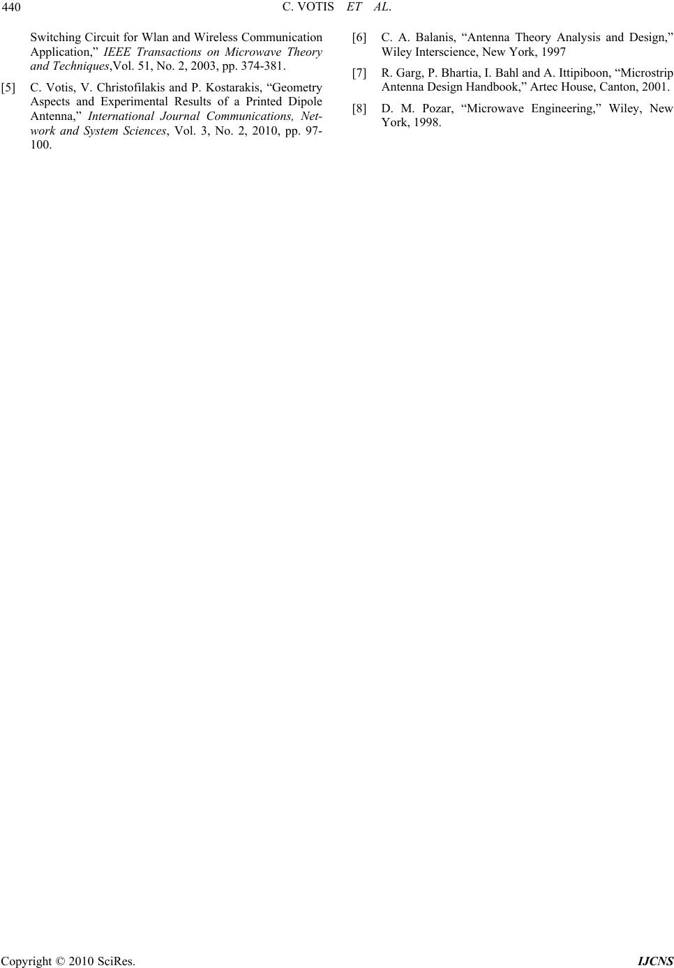 C. VOTIS ET AL. Copyright © 2010 SciRes. IJCNS 440 Switching Circuit for Wlan and Wireless Communication Application,” IEEE Transactions on Microwave Theory and Techniques,Vol. 51, No. 2, 2003, pp. 374-381. [5] C. Votis, V. Christofilakis and P. Kostarakis, “Geometry Aspects and Experimental Results of a Printed Dipole Antenna,” International Journal Communications, Net- work and System Sciences, Vol. 3, No. 2, 2010, pp. 97- 100. [6] C. A. Balanis, “Antenna Theory Analysis and Design,” Wiley Interscience, New York, 1997 [7] R. Garg, P. Bhartia, I. Bahl and A. Ittipiboon, “Microstrip Antenna Design Handbook,” Artec House, Canton, 2001. [8] D. M. Pozar, “Microwave Engineering,” Wiley, New York, 1998. |