Paper Menu >>
Journal Menu >>
 Int. J. Communications, Network and System Sciences, 2010, 3, 425-429 doi:10.4236/ijcns.2010.35055 Published Online May 2010 (http://www.SciRP.org/journal/ijcns/) Copyright © 2010 SciRes. IJCNS A/D Restrictions (Errors) in Ultra-Wideband Impulse Radios Giorgos Tatsis1, Constantinos Votis1, Vasilis Raptis1, Vasilis Christofilakis1,2, Panos Kostarakis1 1Physics Department, University of Ioannina, Ioannina, Greece 2Siemens Enterprise Communications, Enterprise Products Development, Athens, Greece E-mail: {gtatsis, kvotis, vraptis}@grads.uoi.gr basilios.christofilakis@siemens-enterprise.com, kostarakis@uoi.gr Received February 4, 2010; revised March 6, 2010; accepted April 20, 2010 Abstract Ultra-Wideband Impulse Radio (UWB-IR) technologies, although are relatively easy in transmission but they present difficulties in reception, in fact the reception of such waveform is a quite complicated matter. The main reason is that in fully digital receiver the received waveform must be sampled at a rate of several GHz. This paper focuses on the impact of the Analog to Digital (A/D) conversion stage that is used to sam- ple the received waveform. More specifically we focus on the impact of the two main parameters that affect the performance of the Software Defined Radio (SDR) system. These parameters are the bit resolution and the time jittering. The influence of these parameters is deeply examined. Keywords: UWB, Impulse Radio, ADC, Jitter Error, Quantization Error 1. Introduction UWB transmission has recently received great attention in academia and industry for applications in wireless communications. A UWB system is defined as any radio system that has a 10 dB fractional bandwidth larger than 20% of its center frequency, or has a 10 dB bandwidth larger than 500 MHz. It is expected that many ap- proaches used for short-range wireless communications will be revaluated and a new industrial sector with high data rate will be formed. Fully digital receiver for UWB-IR requires the use of A/D conversion and SDR techniques as described below. The RF waveform re- ceived from the antenna is directly digitized from the antenna via an A/D conversion stage. Then the digital information derived from the UWB waveform is handled and processed by a DSP. However, this process, intro- duce new signal distortions, due to the new uncertainties introduced, that are the jitter error and the quantization error. The latter comes exclusively from the bit resolu- tion of the A/D converter, while time jittering comes merely from the aperture jitter of the ADC, and from clock jitter of the sampling circuitry [1,2]. In this paper we examine the impact of those two parameters on the bit error rate performance of an UWB-IR fully digital receiver. In UWB-IR systems a pulse train, consisting of very short pulses and occupying very large spectrum [3], is transmitted. Several modulation schemes are used such as Bi-phase, Pulse Position, On-Off keying etc. [4]. In this paper we choose Binary Pulse Position Modulation (BPPM). We consider transmission through indoor mul- tipath environment [5], in the presence of white Gaussian noise. The performance of the system is evaluated by the bit error probability (BEP) in terms of jitter and quanti- zation noise. An expression of BEP is derived and nume- rically results are presented. 2. Analog to Digital Conversion During the A/D conversion additional noise is produced at the output of the A/D converter due to two main rea- sons: Quantization and Jitter error. The first is illustrated in Figure 1 (a) and it is a result of the difference be- tween the analog, continuous input signal and the digi- tized output of the ADC. The finite ADC resolution gives the form of the stairs-like signal. If an ADC has a bit resolution of N bits, it means that the output signal is coded at 2 N different binary numbers, from 0 to 2 N –1. Let assume that the input signals peak to peak amplitude ( p p V) is the same with the ADC full-scale voltage range. Then the corresponding quantization step is /2 N pp QV. An amplitude value at the input is mapped to the nearest N bit binary number and the  G. TATSIS ET AL. Copyright © 2010 SciRes. IJCNS 426 absolute difference between input-output can be from zero to /2Q, thus the quantization error is from /2Q to /2Q. We assume that the input signal can take any random value within a quantization step, with equal probability. Therefore the distribution of quantiza- tion error is uniform and its probability density function () f x, is shown in Figure 1(b). Obviously, it has a mean of zero and it is easy to prove that the standard deviation of quantization error is /12 qQ , as follows, 32 222 2 22 0 2 122 () 24 12 QQ qQ QQ xfxdxxdx xdx QQQ The second error that concerns our study is called jitter error and it is a result of the non infinite timing precision of the sampling procedure and the ADC imperfections. The fact is that there is an uncertainty at the sampling time which causes an uncertainty at the input voltage of the signal. This effect is shown in Figure 2. Let the input signal at an A/D converter be ()Vt . We focus at the A mp li tu d e Time (a) -Q/2 Q/2 x f (x) 1/Q (b) Figure 1. (a) Digitization of an analog continuous signal (dotted line) to discrete and quantized signal (normal line); (b) Uniform distribution () f x of quantization error x. time 1 t, corresponding at a multiplicate of sampling period. Due to jitter effect the sample taken by the ADC is the one at the time 1 j tt , where j t is a random variable, assuming normally distributed with zero mean and standard deviation j . The corresponding voltage error is then, 11 ()() jj VVtt Vt . By rewriting this expression we have, 11 11 ()() ()() j j jj j Vtt Vt VVtt Vtt t (1) For small j t we can approximate the expression in the brackets with the first derivative of ()Vt [6], and obtaining, 1 ' 1 () () jjj tt dV t VttVt dt (2) 3. Signal Model Description The transmitted pulses have the form of a Gauss mono- cycle, i.e. the first derivative of a standard Gauss pulse. Figure 3 shows a schematic representation of the BPPM modulated transmitted signal. The bit period is f T (fra- me period) and the time offset represents the modu- lation index. Time is divided into frames, the period of V(t) ∆V j t 1 t 1 + ∆t j t ∆t j Figure 2. Jitter error effect. T f T f 00 1 Figure 3. BPPM signaling. 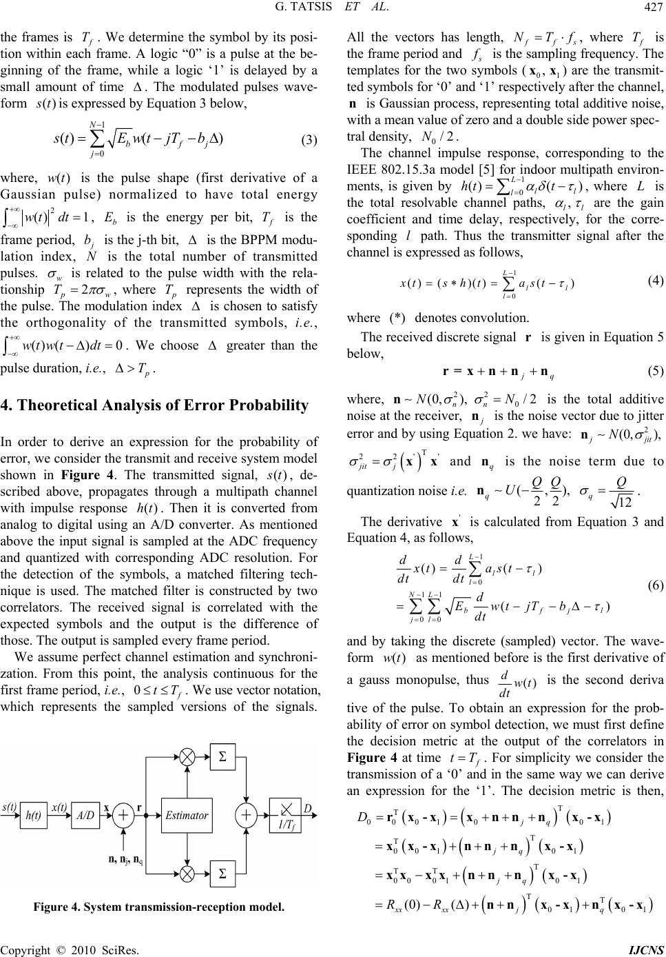 G. TATSIS ET AL. Copyright © 2010 SciRes. IJCNS 427 the frames is f T. We determine the symbol by its posi- tion within each frame. A logic “0” is a pulse at the be- ginning of the frame, while a logic ‘1’ is delayed by a small amount of time . The modulated pulses wave- form () s tis expressed by Equation 3 below, 1 0 () () N bfj j s tEwtjTb (3) where, ()wt is the pulse shape (first derivative of a Gaussian pulse) normalized to have total energy 2 () 1wt dt , b E is the energy per bit, f T is the frame period, j b is the j-th bit, is the BPPM modu- lation index, N is the total number of transmitted pulses. w is related to the pulse width with the rela- tionship 2 p w T , where p T represents the width of the pulse. The modulation index is chosen to satisfy the orthogonality of the transmitted symbols, i.e., () ()0wt wtdt . We choose greater than the pulse duration, i.e., p T. 4. Theoretical Analysis of Error Probability In order to derive an expression for the probability of error, we consider the transmit and receive system model shown in Figure 4. The transmitted signal, () s t, de- scribed above, propagates through a multipath channel with impulse response ()ht. Then it is converted from analog to digital using an A/D converter. As mentioned above the input signal is sampled at the ADC frequency and quantized with corresponding ADC resolution. For the detection of the symbols, a matched filtering tech- nique is used. The matched filter is constructed by two correlators. The received signal is correlated with the expected symbols and the output is the difference of those. The output is sampled every frame period. We assume perfect channel estimation and synchroni- zation. From this point, the analysis continuous for the first frame period, i.e., 0 f tT . We use vector notation, which represents the sampled versions of the signals. Figure 4. System transmission-reception model. All the vectors has length, f fs NTf, where f T is the frame period and s f is the sampling frequency. The templates for the two symbols (01 ,xx) are the transmit- ted symbols for ‘0’ and ‘1’ respectively after the channel, n is Gaussian process, representing total additive noise, with a mean value of zero and a double side power spec- tral density, 0/2N. The channel impulse response, corresponding to the IEEE 802.15.3a model [5] for indoor multipath environ- ments, is given by 1 0 ()( ) L ll l ht t , where L is the total resolvable channel paths, , ll are the gain coefficient and time delay, respectively, for the corre- sponding l path. Thus the transmitter signal after the channel is expressed as follows, 1 0 () ()()() L ll l xtsh tast (4) where (*) denotes convolution. The received discrete signal r is given in Equation 5 below, j q r=xnnn (5) where, 22 0 (0,),/ 2 nn NN n is the total additive noise at the receiver, j n is the noise vector due to jitter error and by using Equation 2. we have: 2 (0, ), j jit N n T 22'' jit j xx and q n is the noise term due to quantization noise i.e. (,), 22 12 qq QQ Q U n. The derivative ' x is calculated from Equation 3 and Equation 4, as follows, 1 0 11 00 ()( ) () L ll l NL bfjl jl dd xt ast dt dt d EwtjTb dt (6) and by taking the discrete (sampled) vector. The wave- form ()wt as mentioned before is the first derivative of a gauss monopulse, thus () dwt dt is the second deriva tive of the pulse. To obtain an expression for the prob- ability of error on symbol detection, we must first define the decision metric at the output of the correlators in Figure 4 at time f tT . For simplicity we consider the transmission of a ‘0’ and in the same way we can derive an expression for the ‘1’. The decision metric is then, T T 0001001 T T 001 01 T TT 00010 1 TT 01 01 (0)( ) jq jq jq xx xxjq D RR rx-xx nnnx-x xx -xnnnx -x xxxxnnnx-x n nx-xnx-x 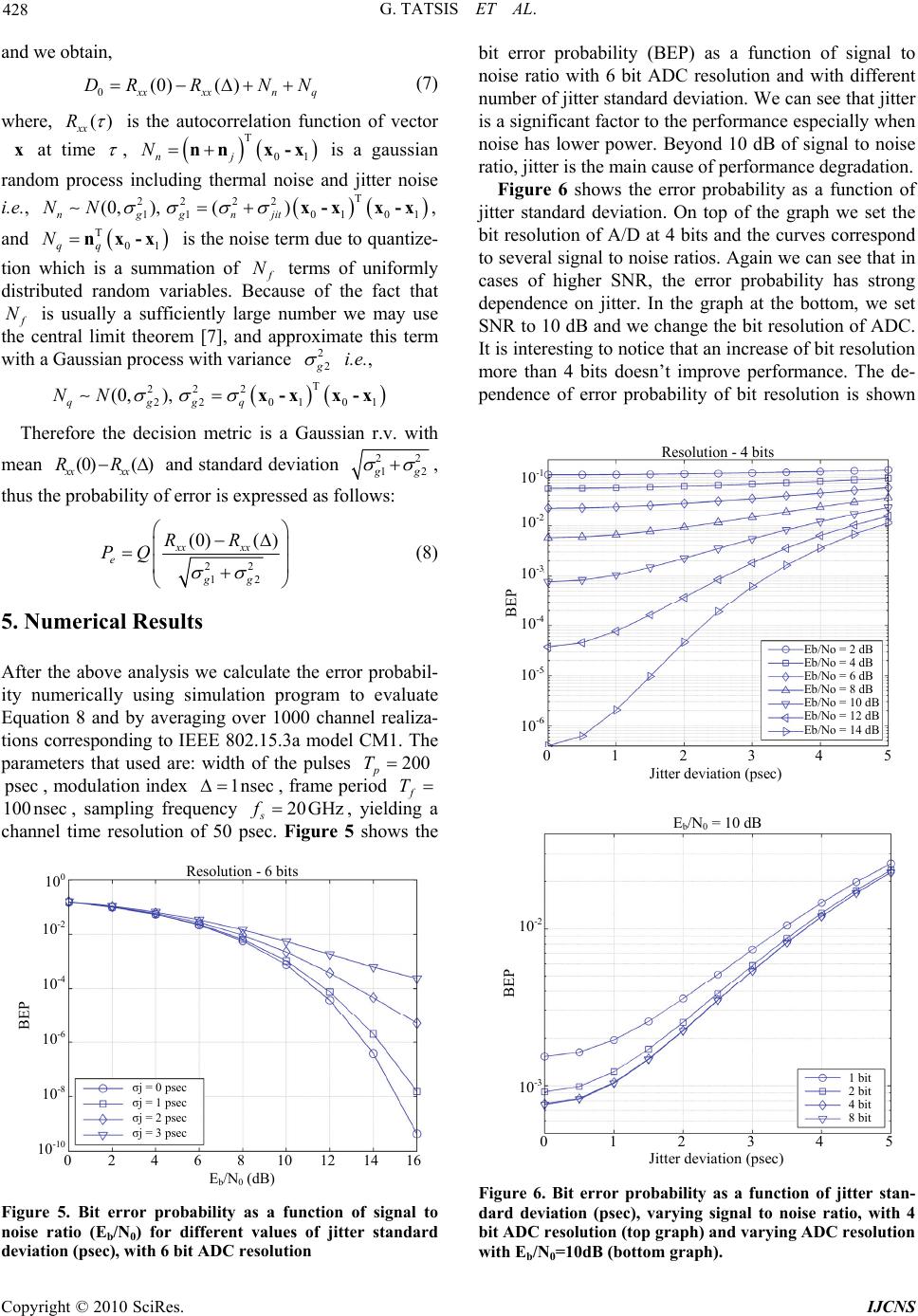 G. TATSIS ET AL. Copyright © 2010 SciRes. IJCNS 428 and we obtain, 0(0)( ) x xxx nq DR RNN (7) where, () xx R is the autocorrelation function of vector x at time , T 01 nj Nnn x-x is a gaussian random process including thermal noise and jitter noise i.e., T 22 22 1101 01 (0,),() nggn jit NN x-xx-x , and T 01 qq Nnx-x is the noise term due to quantize- tion which is a summation of f N terms of uniformly distributed random variables. Because of the fact that f N is usually a sufficiently large number we may use the central limit theorem [7], and approximate this term with a Gaussian process with variance 2 2 g i.e., T 22 2 22 0101 (0, ), qggq NN x-xx-x Therefore the decision metric is a Gaussian r.v. with mean (0)( ) xx xx RR and standard deviation 22 12 g g , thus the probability of error is expressed as follows: 22 12 (0)( ) xx xx e gg RR PQ (8) 5. Numerical Results After the above analysis we calculate the error probabil- ity numerically using simulation program to evaluate Equation 8 and by averaging over 1000 channel realiza- tions corresponding to IEEE 802.15.3a model CM1. The parameters that used are: width of the pulses 200 p T p sec , modulation index 1nsec , frame period f T 100 nsec, sampling frequency 20GHz s f, yielding a channel time resolution of 50 psec. Figure 5 shows the Resolution - 6 bits E b /N 0 ( dB ) BEP 10 0 10 -2 10 -4 10 -6 10 -8 10 -10 0 2 4 6 8 10 12 14 16 σj = 0 psec σj = 1 psec σj = 2 psec σj = 3 psec Figure 5. Bit error probability as a function of signal to noise ratio (Eb/N0) for different values of jitter standard deviation (psec), with 6 bit ADC resolution bit error probability (BEP) as a function of signal to noise ratio with 6 bit ADC resolution and with different number of jitter standard deviation. We can see that jitter is a significant factor to the performance especially when noise has lower power. Beyond 10 dB of signal to noise ratio, jitter is the main cause of performance degradation. Figure 6 shows the error probability as a function of jitter standard deviation. On top of the graph we set the bit resolution of A/D at 4 bits and the curves correspond to several signal to noise ratios. Again we can see that in cases of higher SNR, the error probability has strong dependence on jitter. In the graph at the bottom, we set SNR to 10 dB and we change the bit resolution of ADC. It is interesting to notice that an increase of bit resolution more than 4 bits doesn’t improve performance. The de- pendence of error probability of bit resolution is shown Resolution - 4 bits Jitter deviation (psec) BEP 10 -1 10 -2 10 -3 10 -4 10 -5 10 -6 0 1 2 3 4 5 Eb/No = 2 dB Eb/No = 4 dB Eb/No = 6 dB Eb/No = 8 dB Eb/No = 10 dB Eb/No = 12 dB Eb/No = 14 dB E b /N0 = 10 dB Jitter deviation (psec) BEP 10-2 10-3 0 1 2 3 4 5 1 bit 2 bit 4 bit 8 bit Figure 6. Bit error probability as a function of jitter stan- dard deviation (psec), varying signal to noise ratio, with 4 bit ADC resolution (top graph) and varying ADC resolution with Eb/N0=10dB (bottom graph). 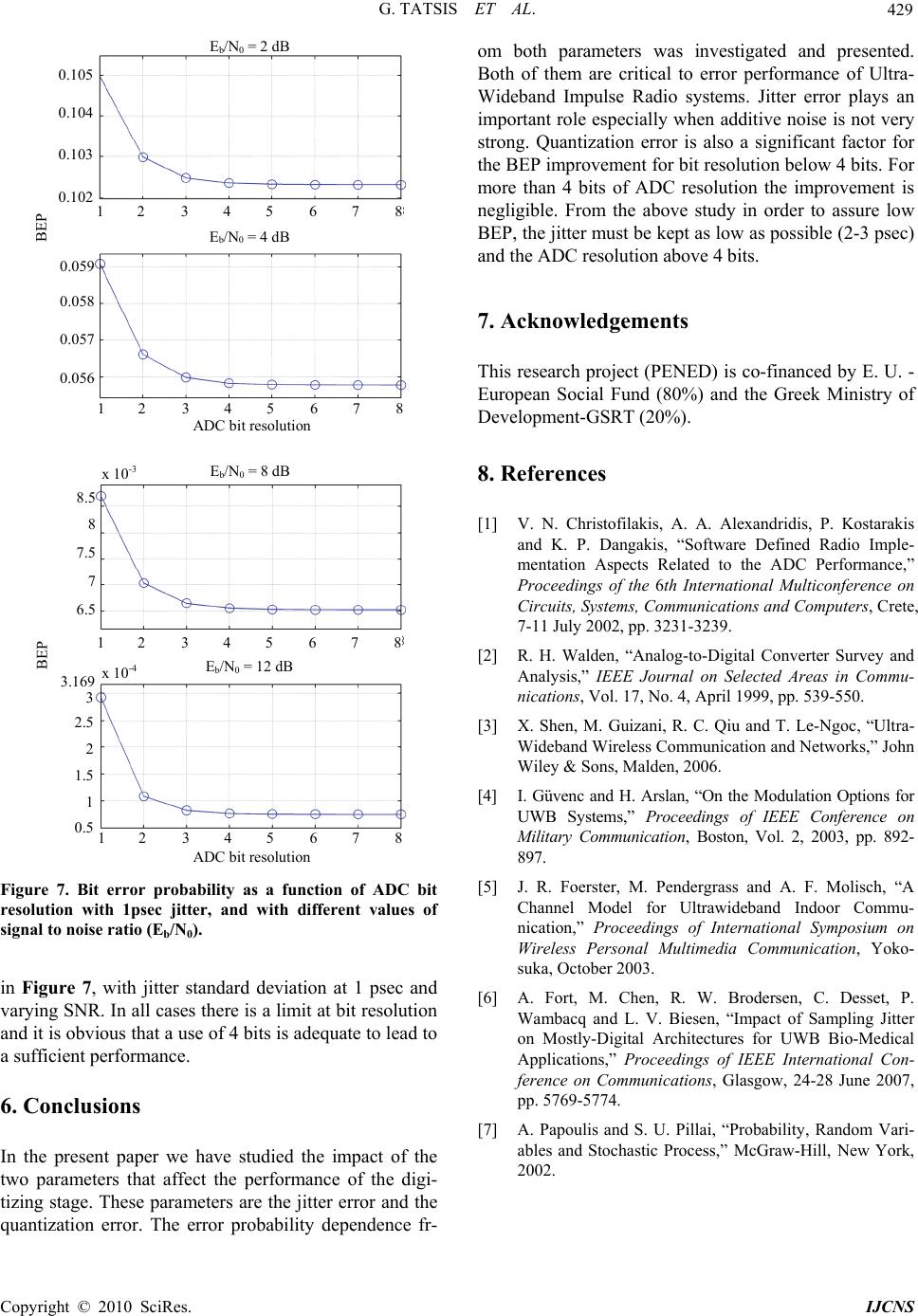 G. TATSIS ET AL. Copyright © 2010 SciRes. IJCNS 429 E b /N0 = 2 dB ADC bit resolution BEP 0.105 0.104 0.103 0.102 1 2 3 4 5 6 7 8 E b /N0 = 4 dB 1 2 3 4 5 6 7 8 0.059 0.058 0.057 0.056 E b /N 0 = 8 dB ADC bit resolution BEP 8.5 8 7.5 7 6.5 1 2 3 4 5 6 7 8 E b /N 0 = 12 dB 1 2 3 4 5 6 7 8 3 2.5 2 1.5 1 0.5 x 10 -3 x 10 -4 3.169 Figure 7. Bit error probability as a function of ADC bit resolution with 1psec jitter, and with different values of signal to noise ratio (Eb/N0). in Figure 7, with jitter standard deviation at 1 psec and varying SNR. In all cases there is a limit at bit resolution and it is obvious that a use of 4 bits is adequate to lead to a sufficient performance. 6. Conclusions In the present paper we have studied the impact of the two parameters that affect the performance of the digi- tizing stage. These parameters are the jitter error and the quantization error. The error probability dependence fr- om both parameters was investigated and presented. Both of them are critical to error performance of Ultra- Wideband Impulse Radio systems. Jitter error plays an important role especially when additive noise is not very strong. Quantization error is also a significant factor for the BEP improvement for bit resolution below 4 bits. For more than 4 bits of ADC resolution the improvement is negligible. From the above study in order to assure low BEP, the jitter must be kept as low as possible (2-3 psec) and the ADC resolution above 4 bits. 7. Acknowledgements This research project (PENED) is co-financed by E. U. - European Social Fund (80%) and the Greek Ministry of Development-GSRT (20%). 8. References [1] V. N. Christofilakis, A. A. Alexandridis, P. Kostarakis and K. P. Dangakis, “Software Defined Radio Imple- mentation Aspects Related to the ADC Performance,” Proceedings of the 6th International Multiconference on Circuits, Systems, Communications and Computers, Crete, 7-11 July 2002, pp. 3231-3239. [2] R. H. Walden, “Analog-to-Digital Converter Survey and Analysis,” IEEE Journal on Selected Areas in Commu- nications, Vol. 17, No. 4, April 1999, pp. 539-550. [3] X. Shen, M. Guizani, R. C. Qiu and T. Le-Ngoc, “Ultra- Wideband Wireless Communication and Networks,” John Wiley & Sons, Malden, 2006. [4] I. Güvenc and H. Arslan, “On the Modulation Options for UWB Systems,” Proceedings of IEEE Conference on Military Communication, Boston, Vol. 2, 2003, pp. 892- 897. [5] J. R. Foerster, M. Pendergrass and A. F. Molisch, “A Channel Model for Ultrawideband Indoor Commu- nication,” Proceedings of International Symposium on Wireless Personal Multimedia Communication, Yoko- suka, October 2003. [6] A. Fort, M. Chen, R. W. Brodersen, C. Desset, P. Wambacq and L. V. Biesen, “Impact of Sampling Jitter on Mostly-Digital Architectures for UWB Bio-Medical Applications,” Proceedings of IEEE International Con- ference on Communications, Glasgow, 24-28 June 2007, pp. 5769-5774. [7] A. Papoulis and S. U. Pillai, “Probability, Random Vari- ables and Stochastic Process,” McGraw-Hill, New York, 2002. |