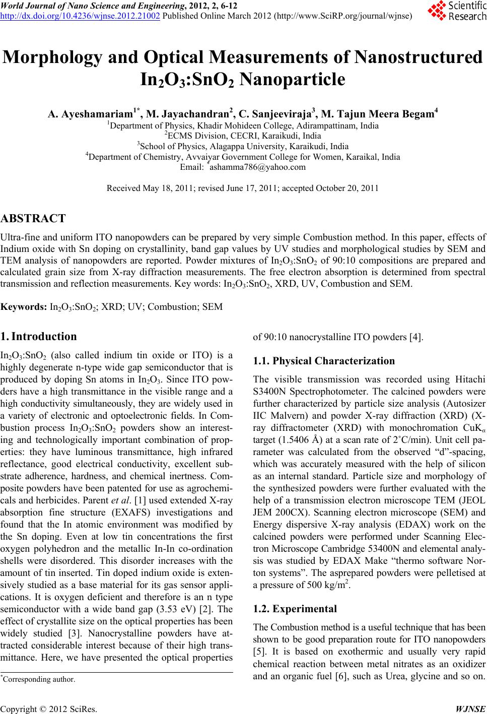
A. AYESHAMARIAM ET AL.
Copyright © 2012 SciRes. WJNSE
12
Lucazeau and M. Roumyantseva, “Structural Characteri-
zation of Nanocrystalline SnO2 by X-Ray and Raman
Spectroscopy,” Journal of Solid State Chemistry, Vol.
135, No. 1, 1998, pp. 78-85. doi:10.1006/jssc.1997.7596
[5] J. H. Kang, J. Y. Kim and D. Y. Jeona, “Synthesis and
Characterization of Orange Emitting SnO2: Eu3+ Phos-
phor by an Optimized Combustion Method,” Journal of
mical Society, Vol. 152, No. 3, pp. H33-the Electroche
H38.
[6] L. E. Shea, J. Mukittrick and O. A. Lopez “Synthesis of
Red-Emitting, Small Particle Size Luminescent Oxides
Using an Optimized Combustion Process,” Journal of the
American Ceramic Society, Vol. 79, No. 12, 1996, pp.
3257-3265. doi:10.1111/j.1151-2916.1996.tb08103.x
[7] S. R. Jain, K. C. Adiga and V. R. P. Verneker, “A New
Approach to Thermochemical Calculations of Condensed
Fuel-Oxidizer Mixtures,” Combustion and Flame, Vol. 40,
1981, pp. 71-79. doi:10.1016/0010-2180(81)90111-5
[8] A. S. Mukasyan, C. Costllo, K. P. Sherlock, D. Lafarga
and A. Varma, “Perovskite Membranes by Aqueous Com-
bustion Synthesis: Synthesis
and Purification Technology
and Properties,” Separation
, Vol. 25, No. 1-3, 2001, pp
117-126. doi: .
10.1016/S1383-5866(01)00096-X
[9] J. H. Kang, J., Proceeding of the
uum Sci-
Y. Kim and D. Y. Jean
3rd International Meeting on information display, Daegu,
2002.
[10] H. Wulff and C. Eggs, “Investigation of Stored Energy in
Plasma Deposited TiNx Films,” Journal of Vac
ence & Technology A, Vol. 15, No. 6, 1997, p. 2938.
doi:10.1116/1.580888
[11] A. R. Stokes, “A Numerical Fourier-Analy
the Correction of Widthsis Method for
s and Shapes of Lines on X-ray
Powder Photographs,” Proceedings of the Physical Soci-
ety, Vol. 6, No. 4, 1948, p. 382.
doi:10.1088/0959-5309/61/4/311
[12] Y. Ohhata, F. Shinoki and S. Yoshida, “Optical Properties
of r.f. Reactive Sputtered Tin-Doped In2O3 Films,” Thin
Solid Films, Vol. 59, No. 2, 1979, pp. 255-261.
doi:10.1016/0040-6090(79)90298-0
[13] J. Tauc, R. Grigorovici and A. Vancu, “Optical Properties
and Electronic Structure of Amorphous Germanium,”
Physica Status Solidi (b), Vol. 15, No. 2, 1966, pp. 627-
637. doi:10.1002/pssb.19660150224
[14] J. Tauc, “Amorphous and Liquid Semiconductors,” In: J.
ed
e Obtained by the Sol-Gel Method
Tauc, Ed., Plenum, New York, 1979.
[15] A. Gurlo, N. Barsan, U. Weimar, M. Ivanovskaya, A.
Taurino and P. Siciliano, “Polycrystalline Well-Shap
Blocks of Indium Oxid
and Their Gas-Sensing Properties,” Chemistry of Mater-
ials, Vol. 15, No. 23, 2003, pp. 4377-4383.
doi:10.1021/cm031114n
[16] P. S. Devi, M. Chatterjee and D
Oxide Nano-Particles through an. Ganguli, “Indium Tin
Emulsion Technique,”
Material Letters, Vol. 55, No. 4, 2002, pp. 205-210.
doi:10.1016/S0167-577X(01)00647-4
[17] S. Ramanan, “Dip coated ITO Thin-Films throu
Gel Process Using Metal Salts,” Th
gh Sol-
in Solid Films, Vol.
389, No. 1-2, 2001, pp. 207-212.
doi:10.1016/S0040-6090(01)00825-2
[18] H. Y. Xu, X. L. Liu, D. L. Cui, M. Li and M. H. Jiang, “A
Novel Method for Improving the Performance of ZnO
Gas Sensors,” Sensors and Actuators B: Chemical, Vol.
114, No. 1, 2006, pp. 301-307.
doi:10.1016/j.snb.2005.05.020