Journal of Applied Mathematics and Physics
Vol.04 No.02(2016), Article ID:63843,7 pages
10.4236/jamp.2016.42046
Correlation between the Low-Temperature Photoluminescence Spectra and Photovoltaic Properties of Thin Polycrystalline CdTe Films
Bozorboy Joboralievich Akhmadaliev, Olmos Muhammaddovidovich Mamatov, Bakhtiyor Zaylobidinovich Polvonov, Nosirjon Khaydarovich Yuldashev
Ferghana Polytechnic Institute, Ferghana, Uzbekistan

Copyright © 2016 by authors and Scientific Research Publishing Inc.
This work is licensed under the Creative Commons Attribution International License (CC BY).
http://creativecommons.org/licenses/by/4.0/


Received 2 January 2016; accepted 23 February 2016; published 26 February 2016
ABSTRACT
A dominant intrinsic luminescence band, which is due to the surface potential barriers of crystalline grains, and an edge doublet, which arises as an LO-phonon repetition of the e-h band, has been revealed in the low-temperature photoluminescence spectra of fine-grained obliquely deposited films. Doping film with In impurity leads to quenching of the doublet band, while further thermal treatment causes activation of the intrinsic band, the half-width and the blue shift of the red edge of which correlates with the maximum value of anomalously high photovoltage generated by the film.
Keywords:
Film Structures, Low-Temperature Photoluminescence, Crystalline Grains, Surface Potential Barriers, Anomalous Photovoltaic Properties, Thermal Treatment, Photocarriers, Intrinsic Luminescence Band, LO-Phonon Repetitions

1. Introduction
Low-temperature photoluminescence (LTPL) spectroscopy is one of the most sensitive and informative optical methods for studying semiconductors and film structures. LTPL spectra of CdTe crystals has been investigated in detail, and new methods for predicting and controlling electrical properties of semiconductor structures have been proposed on their basis. In particular, based on the study of the dynamics of changes in photoluminescence spectra [1] [2] , a method for deep sample purification was developed, and polycrystalline CdTe of stoichiometric composition with a photoluminescence spectrum containing only the exciton component and no impurity contributions was obtained. The electron spectra of CdTe:In [3] and CdTe:Fe [4] solid solutions were investigated by the analyzing the shape of the edge luminescence band under laser excitation. The role of grain boundaries in the formation of properties of coarse-grained cadmium telluride was investigated by photoluminescence microprobe methods; it was shown that the impurity-defect compositions of the boundary and internal regions of single-crystal grains with sizes of 1 - 2 mm are significantly different [5] [6] . However, the influence of structural and point defects on the formation of the photoluminescence (PL) spectrum of fine-grained  semiconductor samples has not been considered to date.
In this paper, we report the results of studying the mechanisms of formation of LTPL spectrum and their relationship with the anomalous photovoltaic (APV) properties of obliquely deposited CdTe and CdTe:In films in dependence of the degree of their structural imperfection. It was found previously [7] [8] that doping with In impurity and subsequent thermal treatment (TT) improve significantly the photovoltaic parameters of CdTe films: the short-circuit photocurrent  increases by two orders of magnitude, and the maximum photo-emf value VAPV increases by an order of magnitude. Here, the intrinsic and edge PL spectra of these films are analyzed at T = 4.2 K. The LTPL spectra of fine-grained polycrystalline CdTe and CdTe:In films with APV properties, in contrast to the spectra of single crystals and coarse-grained polycrystals, were found to contain no contributions from excitons and donor-acceptor pairs (DAPs), which are due to the generation of photo-emf in the boundary regions of crystallites (that leads to stimulation of intrinsic (e-h) luminescence and build-up of longitudinal optical (LO-) phonon repetitions in undoped samples). The red edge of the e-h band exhibits a significant blue shift
 , which is determined by the point and structural defects of crystalline grains. The half-width of this band correlates with the peak value of the anomalously large photovoltage generated in the film.
2. Technology: Experimental Results
The objects of study, pure and In-doped obliquely deposited polycrystalline films with a thickness of  and an area of
 , were obtained from CdTe powder by thermal evaporation in vacuum (residual gas pressure
 ) onto a glass substrate at a temperature
  [7] [8] . The sizes of individual crystallites were
 . CdTe films at room temperature, illuminated by an incandescent lamp with intensity
 , generated photovoltage
  and short-circuit current
 . As- prepared CdTe: In samples with a thickness
  turned out to have a lower resistivity and rather weakly pronounced APV properties
 . However, after a TT at a temperature
  for
for  in air in the presence of coactivator CdCl2 vapor, they generated a photovoltage up to
 , and the short-circuit photocurrent was as high as
 . The photovoltaic parameters of the films practically did not degrade during a year.
When measuring LTPL spectra, film samples were directly immersed in pumped liquid helium at a temperature of 4.2 K. Spectra were recorded on a system based on a DFS-24 spectrometer, operating in the photon- counting mode at a minimum slit width of 0.04 meV. Intrinsic excitation of semiconductor was performed by a 7-mW cw gas-discharge Ar+ laser beam, focused on the CdTe layer surface into a spot 0.4 × 0.4 mm2 in size. The experiment was performed under conditions of normal illumination and close-to-normal emission.
The LTPL spectrum of undoped CdTe film in the vicinity of the fundamental absorption band is presented in Figure 1(a) in comparison with the PL spectrum of pure single-crystal sample from [6] (dotted line), which expands only to the frequency region  and consists of an exciton line
 , DAP line
 , and their LO-phonon repetitions. As can be seen, the CdTe polycrystalline film and CdTe single crystal have radically different LTPL spectra.
The main contributions to the film LTPL are from the radiative recombination of e-h free carriers (A line with a half-width of ) and edge luminescence with a relatively wide doublet structure (B and C emission lines with half-widths of
  and
and , respectively), whereas the exciton and DAP luminescence channels and their phonon repetitions are not observed against the background of the A, B, and C lines. The presence of sharp long-wavelength boundary
  of the intrinsic emission band is indicative of perfect crystal structure of individual grains. Note that the red edge of the A line is blue-shifted by 0.021 eV in comparison with the bottom of the conduction band of CdTe single crystal (the vertical dach-dotted
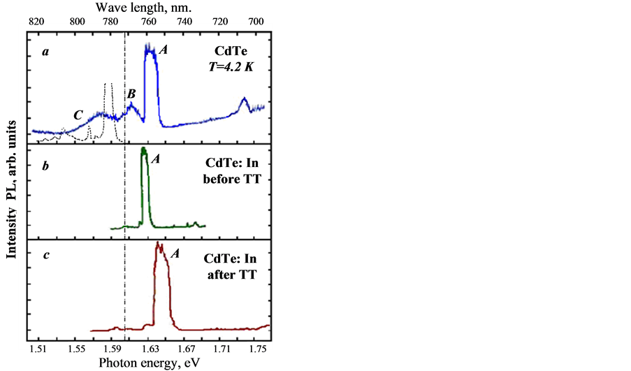
Figure 1. The experimental LTPL spectrum of undoped (a), which is alloyed by In doped CdTe films before (b) and after (c) of the TT. Dashing line is a PL spectrum of undoped monocrystalline CdTe [6], but the dotted line is shown upper border its forbidden band at 4.2 K.
line in Figure 1(a)) at T = 4.2 K ( [9] ). This feature can hardly be explained by, for example, the existence of internal mechanical tensile stress in a thin CdTe film because of the difference in the thermal expansion coefficients or interatomic distances in the film and substrate, which would lead to an increase in the band gap
 .
.
It can be seen in Figure 1(a) that the peak energies of the A, B, and C emission lines differ from the energy of longitudinal optical phonon in CdTe:  [9] . Hence, one can state that the symmetric B line is an LO-repetition, and the C line is a 2LO repetition of the intrinsic A emission band, which, as well as the fundamental band, were absent in the spectra of single crystal and large-crystallite polycrystal at a laser excitation intensity ~0.44 W/cm2. The flat maximum of the C emission line is shifted from the A line by an energy somewhat exceeding
  and has a long-wavelength tail, which indicates that this spectral line is obviously formed as a result of e-h recombination with subsequent emission of
  phonons.
Figure 1(b) shows an LTPL spectrum of a CdTe:In film that was not subjected to TT. One can see that doping a film with indium impurity to a concentration not lower than  distorts to a great extent its LTPL spectrum. First, the half-width of the A line (
 ) is significantly reduced, which correlates with the decrease in VAPV by almost an order of magnitude for an as-prepared CdTe:In film in comparison with undoped CdTe film; second, the B and C lines disappear, as well as the hot PL channel; and, third, the red edge of the A line is red-shifted by
 . Apparently, donor substitutional (InCd) or interstitial (Ini) impurities [9] [10] in fine-grained CdTe form an efficient nonradiative recombination channel, thus reducing strongly the role of LO and LA phonons.
The LTPL spectrum of the CdTe:In film subjected to TT under optimal conditions does not change radically (Figure 1(c)). However, it should be note that TT leads to broadening of the A line by a factor of almost 3 , in correspondence with the increase in VAPV to
  and blue shift of the A-line red edge by ~11 meV in comparison with the unannealed CdTe:In film.
3. Discussion
Let us analyze qualitatively the mechanism of formation of the A line in Figure 1 and interpret its main parameters in dependence of technological factors. We will consider the photoexcitation of a fine-grained semiconductor from the intrinsic absorption region with intensity L0. It is known [11] that, when considering the emission from polycrystalline samples, one should arbitrarily distinguish the contributions from the grain-boundary region (GBR), space-charge region (SCR), and quasi-neutral region (QNR):
 (1)
(1)
where  is the quantum yield. Obviously, in coarse-grained samples (
 , where d is the linear crystallite size and
  is the Debye screening length), the QNR plays a key role, and the problem under consideration is reduced to the well-known case of bulk photoluminescence. However, in fine-grained
  polycrystalline films, the GBR and SCR contributions may be dominant, while QNR does not affect much the formation of LTPL.
As can be seen in Figure 1(a), intrinsic emission (dotted line in [6] ) is not observed in pure CdTe single crystals excited by a laser beam of specified intensity . The reason is that the (e-h)-radiative lifetime
  of photocarriers exceeds greatly their lifetimes
  determined by the formation of excitons or phonon emission. The total lifetime of a nonequilibrium electron is given by the expression
 (2)
(2)
where  are the lifetimes of electron in a given energy state, related to the formation of LO phonons, LA phonons, excitons, and DAPs, respectively, and τM is the Maxwell relaxation time. The A-line half-width
  corresponds to
 . Therefore, the observed LTPL spectrum of CdTe film with APV properties obviously corresponds to the reverse situation:
 , as is evidenced by the absence of exciton- and DAP-emission channels in the spectrum. On the other hand, the Maxwell relaxation time
  in high-resistivity samples (objects of our study) is rather long; therefore, the lifetimes of photocarriers in the corresponding bands are mainly determined, according to (2), by the interband radiative recombination
 . This is, apparently, the main cause of the intrinsic PL build-up and suppression of exciton emission in fine-grained polycrystalline direct-gap semiconductors of the CdTe type. In the case of weak surface recombination, the SCR contribution to PL may be dominant.
It should be noted that surface PL and photo-emf always coexist in fine-grained polycrystals under certain conditions. Let us consider a structural model (Figure 2) of an obliquely deposited fine-grained  polycrystalline film. Within this model, crystallites, their boundaries, and pores between them in the electric current transmission direction are considered to form a linear periodic chain of semiconductor-insulator-semicon- ductor (SIS) layers with symmetric surface potential barriers, connected in series. Under illumination, each elementary SIS cell, due to the absorption of light in asymmetric SCRs and spatial separation of photocarriers, ge-

Figure 2. The band of diagram energy of the linear chain semiconductor crystalline grains with asymmetric potential barriers among intercrystalline interface (IL), at illumination by light, bring to APV and PL generation.
nerates not only PL but also a low surface photo-emf , where
 ,
,  are the contact potential differences between neighboring grains in darkness and under illumination, respectively; e is the elementary charge; and
  and
and  are, respectively, the heights of surface potential barriers on the left and right sides of the insulating layer (IL) before and after illumination. Then, it is natural that a linear SIS chain generates high-voltage photo-emf
  (N is the number of SIS cells). If the potential barriers at grain boundaries are symmetric, or the film is sufficiently thick, or the film photoconductivity is high, the APV effect is absent because of shunting SIS with resistances
  or
or  (Figure 3), although surface PL may occur in this case.
Strictly speaking, the PL of a polycrystalline film is formed at different depths and microregions, based on different mechanisms of radiative recombination. Thus, it is rather difficult to perform exact analytical calculation of the PL spectrum. However, some rough approximations can be made based on formula (1) and the above physical considerations. In particular, preliminary quantitative analysis of the spectra of A emission line shows that it can be described in the first approximation by the formula
 (3)
(3)
where A is a constant determined by the film type and the excitation conditions;  is the band gap of CdTe single crystal; k is the Boltzmann constant;
  is the average characteristic temperature of photocarriers, which differs significantly from lattice temperature T; and
  is the difference between the red edge of the A line and
 . Naturally, the second and third factors in the right-hand side of (3) are due to the densities of states in simple bands and quasi-equilibrium photocarrier distribution functions.
The theoretical (according to (3)) and experimental spectra of the fundamental LTPL band of fine-grained CdTe and CdTe:In films with APV properties are compared in Figure 4. The values of the parameters  are chosen based on the blue shift of the red edge of the A line from the experimental spectra in Figures 1(a)-(c):
  (curve 1 for a pure CdTe film), 17 meV (curve 2, CdTe:In without TT), and 29 meV (curve 3, CdTe:In after TT). One can see that the calculated spectral lines 1 - 3 are in good agreement with the experimental results. However, the short-wavelength edges of the spectra differ significantly. The experimental data demonstrate stronger thermalization of hot photocarriers with a characteristic temperature
 , which suggests the existence of additional scattering channels for high-energy nonequilibrium free carriers.
A simple calculation shows that the spectral half-width of the A line,  , is directly proportional to the photocarrier temperature, which determines the blue shift of its red edge,
 . This is in qualitative agreement with the changes in the spectral characteristics of the A line in Figures 1(a)-(c). Doping a CdTe film with In impurity leads to a decrease in
  and
and ; thus, one can see in Figure 1(b) that
  decreases by 3 - 5 meV and
  decreases by a factor of almost 3 (to 6 meV). According to the data of Figure 3, resistances
 ,
,  , and
, and  also decrease, and the film passes to a state with lower resistivity, as a result of which short-circuit photocurrent
  increases and the maximum value of photo-emf
  decreases. Subsequent optimal TT, due to the self-compensa- tion processes [12] , transforms the film to the high-resistivity state (not only due to the rise in microresistances

Figure 3. The equivalent electrical circuit of one structured cell SIS under the action of light, generating photo-emf.  -surface photo-emf, generated by APV on the left and on the right from the interface;
  -shunting their resistance in favor of the surface conductivity,
  -shunting resistance of the channel conductivity; C and
  -electro-ca- pacitance and active resistance of the interface.
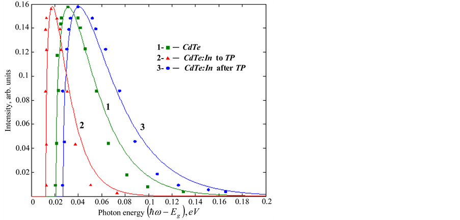
Figure 4. The comparison of theoretical (the utter curves) and experimental (points) spectrums of LTPL fundamental band of fine grained CdTe APV films at .
.
but also as a result of the increase in  and the SCR expansion). Figure 1(c) shows that
  increases to 17 meV, while
  rises to 29 meV.
4. Conclusions
1) The LTPL spectra of fine-grained CdTe films excited by a cw gas-discharge Ar+ laser contains a fundamental emission band with a half-width  (A line) and its LO- and 2LO-phonon repetitions.
2) A blue shift of the red edge of the A line was revealed, which was related to the e-h recombination of hot photocarriers, separated by the electric field of the boundary SCRs in crystallites. Shift  correlates with the spectral half-width
 , which depends on the structural defects of the film.
3) A correlation was found between the LTPL spectrum and the APV properties of CdTe and CdTe:In films. The intrinsic luminescence band is due to the presence of potential barriers at grain boundaries, which generate surface photo-emfs; the asymmetry of the latter results in APV properties. Doping with In donor impurity suppresses the role of LO and LA phonons in the processes of relaxation of hot photocarriers in energy and, thus, leads to quenching of the doublet band. Further TT of an obliquely deposited film stimulates the asymmetry of potential barriers at grain boundaries, which manifests itself in the inhomogeneous broadening and sharp activation of the intrinsic band, the half-width of which  and the shift of the edge of which
  is related to the maximum value of photovoltage
 .
.
The method of joint analysis of the LTPL spectra and photoelectric properties of fine-grained CdTe polycrystals, proposed in this study, can successfully be used to investigate properties of other semiconductor film structures.
Cite this paper
Bozorboy JoboralievichAkhmadaliev,Olmos MuhammaddovidovichMamatov,Bakhtiyor ZaylobidinovichPolvonov,Nosirjon KhaydarovichYuldashev, (2016) Correlation between the Low-Temperature Photoluminescence Spectra and Photovoltaic Properties of Thin Polycrystalline CdTe Films. Journal of Applied Mathematics and Physics,04,391-397. doi: 10.4236/jamp.2016.42046
References
- 1. Kvit, A.V., Klevkov, Yu.V., Medvedov, S.A., Bagaev, V.S., Perestoronin, A. and Plotnikov, A.F. (2000) Evolution of Photoluminescence Spectra of Stoichiometric CdTe: Dependence on the Purity of Starting Components. Semiconductors, 34, 17-20.
http://dx.doi.org/10.1134/1.1187955 - 2. Bagaev, V.S., Klevlov, Yu.V., Kolosov, S.A., Krivobok, V.S. and Shepeli, A.A. (2010) Optical and Electrophysical Properties of Defects in High-Purity CdTe. Physics of the Solid State, 52, 37-42.
http://dx.doi.org/10.1134/S1063783410010075 - 3. Ushakov, V.V. and Klevkov, Yu.V. (2003) Microphotoluminescence Spectra of Cadmium Telluride Grown under Nonequilibrium Conditions. Electronic and Optical Properties of Semiconductors, 37, 1042-1046.
- 4. Ushakov, V.V. and Klevkov, Yu.V. (2003) Effect of Grain Boundaries on the Properties of Cadmium Telluride Grown under Nonequilibrium Conditions. Semiconductors, 37, 1259-1263.
http://dx.doi.org/10.1134/1.1626204 - 5. Veleschuk, V.P., Baydullaeva, A., Vlasenko, A.I., Gnatyuk, V.A., Dauletmuratov, B.K., Levickiy, S.N., Lyashenko, O.V. and Aoki, T. (2010) Mass Transfer of Indium in the In-CdTe Structure under Nanosecond Laser Irradiation. Physics of the Solid State, 52, 439-445.
- 6. Permogorov, S.A., Surkova, T.P. and Tenishev, A.N. (1998) Exciton Luminescence of Cd1-xFexTe Solid Solution. Physics of the Solid State, 40, 826-828.
http://dx.doi.org/10.1134/1.1130412 - 7. Karimov, M.A. and Yuldashev, N.Kh. (2007) Obliquely Deposited CdTe:In Films with Anomalous Photovoltaic Properties. Journal Russian Academy of Science: Physics, 71, 1151-1153.
- 8. Karimov, M.A. and Yuldashev, N.Kh. (2006) Indium Admixture Influence Onphoto-Voltaic Properties of Slanting Deposited Films CdTe. Physical Surface Engineering, 2, 58-62.
- 9. Gavrilenko, V.I., Grehov, A.M., Korbutyak, D.V. and Litovchenko, V.G. (1987) The Optical Features of Semiconductors. The Reference Book, Naukova, Kiev, 410, 414.
- 10. Georgobiani, A.N. and Sheynkman, M.K. (1986) In b.: Physics of the Joins. Science, Moscow, Exhibit, 292.
- 11. Zuev, V.A., Sheinkman, A.V. and Tolpygo, K.B. (1977) Nonequlirium Surface Processes in Semiconductors and Semiconductor Instruments. Soviet Radio, Moscow, 116.
- 12. Matveev, O.A. and Terentev, A.I. (1998) Self-Compensation in CdTe〈Cl〉 in the Presence of Phase Equilibrium of the System Crystal-Cadmium (Tellurium) Vapor. Semiconductors, 32, 159-162.
http://dx.doi.org/10.1134/1.1187335