Paper Menu >>
Journal Menu >>
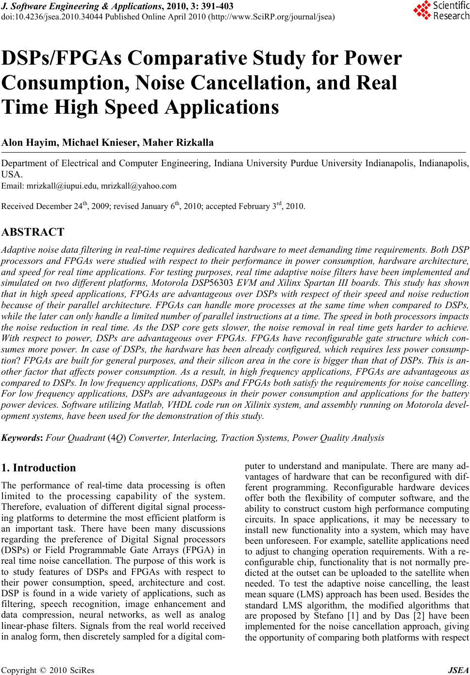 J. Software Engineering & Applications, 2010, 3: 391-403 doi:10.4236/jsea.2010.34044 Published Online April 2010 (http://www.SciRP.org/journal/jsea) Copyright © 2010 SciRes JSEA 391 DSPs/FPGAs Comparative Study for Power Consumption, Noise Cancellation, and Real Time High Speed Applications Alon Hayim, Michael Knieser, Maher Rizkalla Department of Electrical and Computer Engineering, Indiana University Purdue University Indianapolis, Indianapolis, USA. Email: mrizkall@iupui.edu, mrizkall@yahoo.com Received December 24th, 2009; revised January 6th, 2010; accepted February 3rd, 2010. ABSTRACT Adaptive noise data filtering in real-time requ ires dedicated hardware to meet deman ding time requ irements. Both DSP processors and FPGAs were studied with respect to their performance in power consumption, hardware architecture, and speed for real time app lications. For testing purposes, real time adaptive noise filt ers have been implemented and simulated on two different platforms, Motorola DSP56303 EVM and Xilinx Spartan III boards. This study has shown that in high speed applications, FPGAs are advantageous over DSPs with respect of their speed and noise reduction because of their parallel architecture. FPGAs can handle more processes at the same time when compared to DSPs, while the later can only handle a limited number of parallel instructions at a time. The speed in both processors impacts the noise reduction in real time. As the DSP core gets slower, the noise removal in real time gets harder to achieve. With respect to power, DSPs are advantageous over FPGAs. FPGAs have reconfigurable gate structure which con- sumes more power. In case of DSPs, the hardware has been already configured, which requires less power consump- tion? FPGAs are built for general purposes, and their silicon area in the core is bigger than that of DSPs. This is an- other factor that affects power consumption. As a result, in high frequency applications, FPGAs are advantageous as compared to DSPs. In lo w frequency a pplication s, DSPs and FPGAs bo th satisfy the requirements for no ise cancelling. For low frequency applications, DSPs are advantageous in their power consumption and applications for the battery power devices. Softwa re utilizing Ma tlab, VHDL code run on Xilin ix system, and assembly running on Motoro la devel- opment systems, have been used for the demonstration of this study. Keywords: Four Quadrant (4Q) Converter, Interlacing, Traction Systems, Power Quality Analysis 1. Introduction The performance of real-time data processing is often limited to the processing capability of the system. Therefore, evaluation of different digital signal process- ing platforms to determine the most efficient platform is an important task. There have been many discussions regarding the preference of Digital Signal processors (DSPs) or Field Programmable Gate Arrays (FPGA) in real time noise cancellation. The purpose of this work is to study features of DSPs and FPGAs with respect to their power consumption, speed, architecture and cost. DSP is found in a wide variety of applications, such as filtering, speech recognition, image enhancement and data compression, neural networks, as well as analog linear-phase filters. Signals from the real world received in analog form, then discretely sampled for a digital com- puter to understand and manipulate. There are many ad- vantages of hardware that can be reconfigured with dif- ferent programming. Reconfigurable hardware devices offer both the flexibility of computer software, and the ability to construct custom high performance computing circuits. In space applications, it may be necessary to install new functionality into a system, which may have been unforeseen. For example, satellite applications need to adjust to changing operation requirements. With a re- configurable chip, functionality that is not normally pre- dicted at the outset can be uploaded to the satellite when needed. To test the adaptive noise cancelling, the least mean square (LMS) approach has been used. Besides the standard LMS algorithm, the modified algorithms that are proposed by Stefano [1] and by Das [2] have been implemented for the noise cancellation approach, giving the opportunity of co mparing both platforms with respect 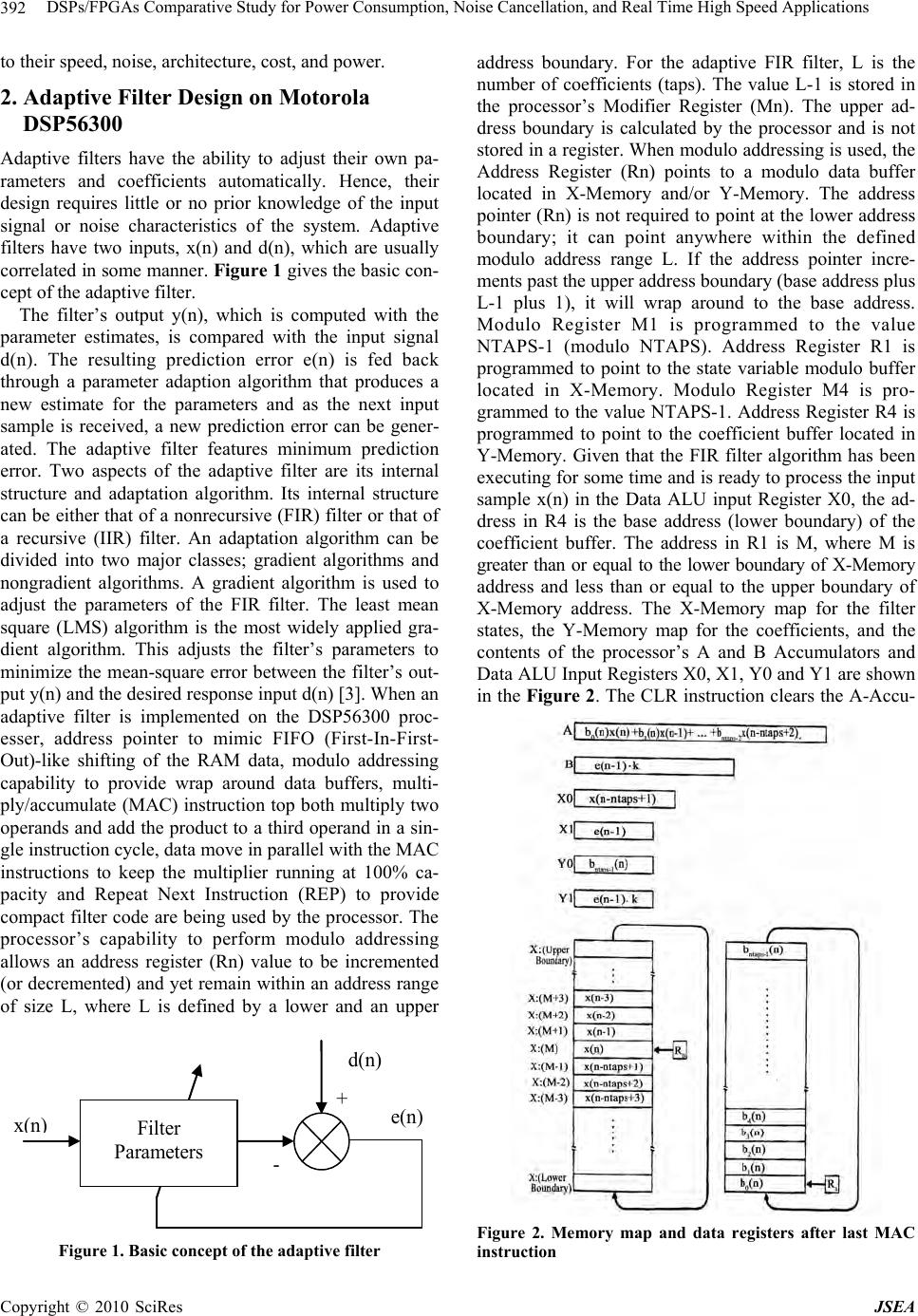 DSPs/FPGAs Compara tive Study for Power Consumption, Noise Cancellation, and Real Time High Speed Applications 392 to their speed, noise, architecture, cost, and power. 2. Adaptive Filter Design on Motorola DSP56300 Adaptive filters have the ability to adjust their own pa- rameters and coefficients automatically. Hence, their design requires little or no prior knowledge of the input signal or noise characteristics of the system. Adaptive filters have two inputs, x(n) and d(n), which are usually correlated in some manner. Figure 1 gives the basic con- cept of the adaptive filter. The filter’s output y(n), which is computed with the parameter estimates, is compared with the input signal d(n). The resulting prediction error e(n) is fed back through a parameter adaption algorithm that produces a new estimate for the parameters and as the next input sample is received, a new prediction error can be gener- ated. The adaptive filter features minimum prediction error. Two aspects of the adaptive filter are its internal structure and adaptation algorithm. Its internal structure can be either that of a nonrecursive (FIR) filter or that of a recursive (IIR) filter. An adaptation algorithm can be divided into two major classes; gradient algorithms and nongradient algorithms. A gradient algorithm is used to adjust the parameters of the FIR filter. The least mean square (LMS) algorithm is the most widely applied gra- dient algorithm. This adjusts the filter’s parameters to minimize the mean-square error between the filter’s out- put y(n) and the desired respon se input d(n) [3]. When an adaptive filter is implemented on the DSP56300 proc- esser, address pointer to mimic FIFO (First-In-First- Out)-like shifting of the RAM data, modulo addressing capability to provide wrap around data buffers, multi- ply/accumulate (MAC) instruction top both multiply two operands and ad d the product to a third operand in a sin- gle instruction cycle, data move in parallel with the MAC instructions to keep the multiplier running at 100% ca- pacity and Repeat Next Instruction (REP) to provide compact filter code are being used by the processor. The processor’s capability to perform modulo addressing allows an address register (Rn) value to be incremented (or decremented) and yet remain within an address range of size L, where L is defined by a lower and an upper x ( n ) d ( n ) + - e(n) Filter Parameters Figure 1. Basic concep the adaptive filter addressis the t of boundary. For the adaptive FIR filter, L number of coefficients (taps). The value L-1 is stored in the processor’s Modifier Register (Mn). The upper ad- dress boundary is calculated by the processor and is not stored in a register. When modulo addressing is used, the Address Register (Rn) points to a modulo data buffer located in X-Memory and/or Y-Memory. The address pointer (Rn) is not required to point at the lower address boundary; it can point anywhere within the defined modulo address range L. If the address pointer incre- ments past the upper address boundary (base address plus L-1 plus 1), it will wrap around to the base address. Modulo Register M1 is programmed to the value NTAPS-1 (modulo NTAPS). Address Register R1 is programmed to point to the state variable modulo buffer located in X-Memory. Modulo Register M4 is pro- grammed to the value NTAPS-1. Address Register R4 is programmed to point to the coefficient buffer located in Y-Memory. Given that the FIR filter algorithm has been executing for some time and is ready to process the input sample x(n) in the Data ALU input Register X0, the ad- dress in R4 is the base address (lower boundary) of the coefficient buffer. The address in R1 is M, where M is greater than or equal to the lower boundary of X-Memory address and less than or equal to the upper boundary of X-Memory address. The X-Memory map for the filter states, the Y-Memory map for the coefficients, and the contents of the processor’s A and B Accumulators and Data ALU Input Registers X0, X1, Y0 and Y1 are shown in the Figure 2. The CLR instruction clears the A-Accu- Figure 2. Memory map and data registers after last MAC instruction Copyright © 2010 SciRes JSEA 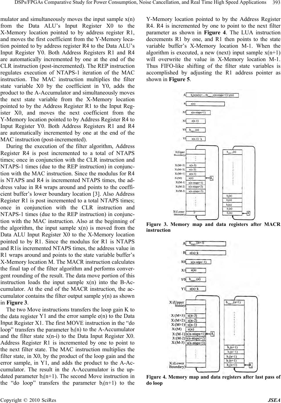 DSPs/FPGAs Compara tive Study for Power Consumption, Noise Cancellation, and Real Time High Speed Applications393 tim Y1 and the error sample e(n) to the Data In mulator and simultaneously moves the input sample x(n) from the Data ALU’s Input Register X0 to the X-Memory location pointed to by address register R1, and moves the first coefficient from the Y-Memory loca- tion pointed to by address register R4 to the Data ALU’s Input Register Y0. Both Address Registers R1 and R4 are automatically incremented by one at the end of the CLR instruction (post-in cremented). The REP instru ction regulates execution of NTAPS-1 iteration of the MAC instruction. The MAC instruction multiplies the filter state variable X0 by the coefficient in Y0, adds the product to the A-Accumulator and simultaneously moves the next state variable from the X-Memory location pointed to by the Address Register R1 to the Input Reg- ister X0, and moves the next coefficient from the Y-Memory location pointed to by Address Register R4 to Input Register Y0. Both Address Registers R1 and R4 are automatically incremented by one at the end of the MAC instruction (post-incremented). During the execution of the filter algorithm, Address Register R4 is post incremented to a total of NTAPS es; once in conjunction with the CLR instruction and NTAPS-1 times (due to the REP instruction) in conjunc- tion with the MAC instruction. Since the modulus for R4 is NTAPS and R4 is incremented NTAPS times, the ad- dress value in R4 wraps around and points to the coeffi- cient buffer’s lower boundary location [3]. Also Address Register R1 is post incremented to a to tal NTAPS times; once in conjunction with the CLR instruction and NTAPS-1 times (due to the REP instruction) in conjunc- tion with the MAC instruction. Also at the beginning of the algorithm, the input sample x(n) is moved from the Data ALU Input Register X0 to the X-Memory location pointed to by R1. Since the modulus for R1 is NTAPS and R1is incremented NTAPS times, the address value in R1 wraps aroun d and points to the state variable buffer’s X-Memory location M. The MACR instru ction calculates the final tap of the filter algorithm and performs conver- gent rounding of the result. The data move portion of this instruction loads the input sample x(n) into the B-Ac- cumulator. At the end of the MACR instruction, the ac- cumulator contains the filter output sample y(n) as shown in Figure 3. The two Move instructions transfers th e loop gain K to the data register put Register X1. The first MOVE instruction in the “do loop” transfers the parameter bi(n) to th e A-Accumulator and the filter state x(n-i) to the Data Input Register X0. Address Register R1 is incremented by one to point to the next filter state. The MAC instruction multiplies the filter state, in X0, by the product of the loop g ain and the error sample, in Y1, and adds the product to the A-Ac- cumulator. The result in the A-Accumulator is the up- dated parameter bi(n+1). The second Move instruction in the “do loop” transfers the parameter bi(n+1) to the Y-Memory location pointed to by the Address Register R4. R4 is incremented by one to point to the next filter parameter as shown in Figure 4. The LUA instruction decrements R1 by one, and R1 then points to the state variable buffer’s X-Memory location M-1. When the algorithm is executed, a new (next) input sample x(n+1) will overwrite the value in X-Memory location M-1. Thus FIFO-like shifting of the filter state variables is accomplished by adjusting the R1 address pointer as shown in Figure 5. Figure 3. Memory map and data registers after MACR instruction Figure 4. Memory map and data registers after last pass of do loop Copyright © 2010 SciRes JSEA 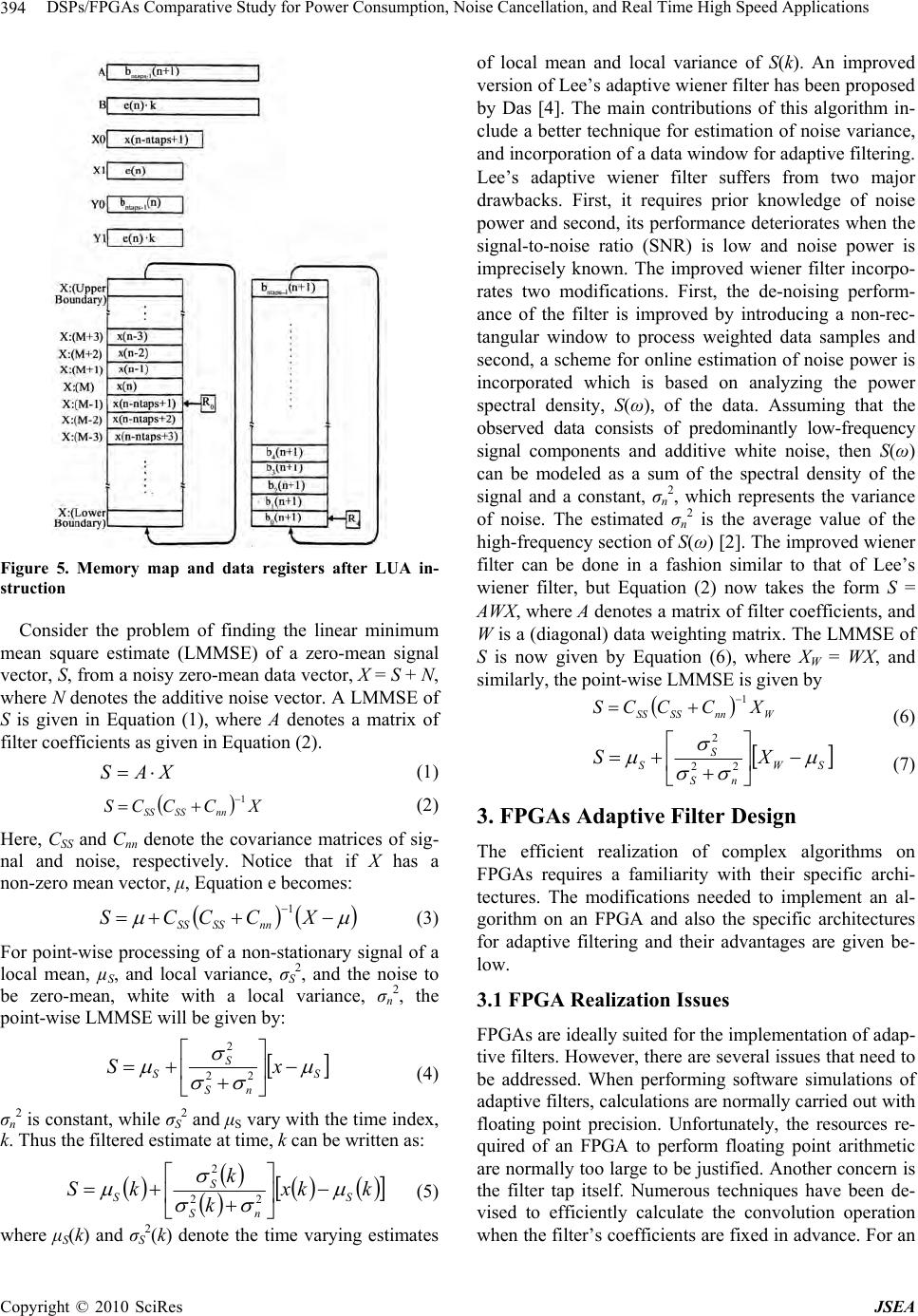 DSPs/FPGAs Compara tive Study for Power Consumption, Noise Cancellation, and Real Time High Speed Applications 394 Figure 5. Memory map and data registers after LUA in- struction Consider the problem of finding the linear minimum mean square estimate (LMMSE) of a zero-mean signal vector, S, from a noisy zero-mean data vector, X = S + N, where N denotes the additive noise vector. A LMMSE of S is given in Equation (1), where A denotes a matrix of filter coefficients as given in Equation (2). Here, CSS and Cnn denote the covariance matrices of sig- nal and noise, respectively. Notice that if X has a non-zero mean vector, μ, Equation e becomes: For point-wise processing of a non-stationary signal of a local mean, µS, and local variance, σS2, and the noise to be zero-mean, white with a local variance, σn2, the point-wise LMMSE will be given by: XAS (1) XCCCS nnSSSS 1 (2) XCCCS nnSSSS 1 (3) S nS S SxS 2 22 (4) σn2 is constant, while σS2 and μS vary with the time index, k. Thus the filtered estimate at time, k can be written as: kkx k k kS S nS S S 22 2 (5) where μ(k) and σ2(k) d S S of local mean and local variance ad filtering. Lee’s adaptive wiener filter suffers from oising perform- ance of the filter is improved by introducing a non-rec- tangular window to process weighted dat second, a scheme for online estimation of noise power is observed data consists of predominantly low-frequency signal components and additive white noise, the can be modeled as a sum of the spectral density of the enote the time varying estimates of S(k). An improved version of Lee’s aptive wiener filter has been propo sed by Das [4]. The main contributions of this algorithm in- clude a better technique for estimation of noise variance, and incorporation of a d ata win dow for ad ap tive two major drawbacks. First, it requires prior knowledge of noise power and second, its performance deteriorates when the signal-to-noise ratio (SNR) is low and noise power is imprecisely known. The improved wiener filter incorpo- rates two modifications. First, the de-n a samples and incorporated which is based on analyzing the power spectral density, S(ω), of the data. Assuming that the n S(ω) signal and a constant, σn2, which represents the variance of noise. The estimated σn2 is the average value of the high-frequency section of S(ω) [2]. The improved wiener filter can be done in a fashion similar to that of Lee’s wiener filter, but Equation (2) now takes the form S = AWX, where A denotes a matrix of filter coefficients, and W is a (diagonal) data weighting matrix. The LMMSE of S is now given by Equation (6), where XW = WX, and similarly, the point-wise LMMSE is given by WnnSSSS XCCCS1 (6) SW nS S SXS 22 2 (7) 3. FPGAs Adaptive Filter Design The efficient realization of complex algorithms on FPGAs requires a familiarity with their specific archi- tectures. The modifications needed to implement an al- gorithm on an FPGA and also the specific architectures for adaptive filtering and their advantages are given be- low. 3.1 FPGA Realization Issues FPGAs are ideally suited for the implementa tion of ad ap- tive filters. However, there are several issues that need to be addressed. When performing software simulations of adaptive filters , calculations are n ormally carried out with floating point precision. Unfortunately, the resources re- quired of an FPGA to perform floating point arithmetic are normally too large to be justified. A the filter tap itself. Numerous techniques have been de- vised to efficiently calculate the convolution when the filter’s coefficients are fixed in advan nother concern is operation ce. For an Copyright © 2010 SciRes JSEA  DSPs/FPGAs Compara tive Study for Power Consumption, Noise Cancellation, and Real Time High Speed Applications395 r time, these ugh computing floatin g point arithmetic in FPGA is d with the inclusion of costly in terms of deci- decimal places is ade- for a given algorithm to s only four bits. For simple convolution, then dividing the output adaptive filter whose coefficients chan ge ove methods will not work or need to be modified signifi- cantly [5]. The reconfigurable filter tap is the most im- portant issue for high performance adaptive filter archi- tecture, and as such it will be discussed at length. 3.2 Finite Precision Effects Altho possible, it is usually accomplishe custom floating point units, which are logic resources. Therefore, a small number of floating point units can be used in the entire design, and must be shared between processes. This does not take full advan- tage of the parallelization that is possible with FPGAs and is therefore not the most efficient method. All calcu- lation should therefore be mapped into fixed point only, but this can introduce some errors. The main errors in DSP include ADC quantization error, coefficient quanti- zation error, overflow error caused impermissible word length, and round off error. The other three issues will be addressed later. 3.2.1 Scale Factor Adjustment A suitable compromise for dealing with the loss of preci- sion when transitioning from a floating point to a fixed- point representation is to keep a limited number of mal digits. Normally, two to three quate, but the number required converge must be found through experimentation. When performing software simulations of a digital filter for example, it is determined that two decimal places is suf- ficient for accurate data processing. This can easily be obtained by multiplying the filter’s coefficients by 100 and truncating to an integer value. Dividing the output by 100 recovers the anticipated valu e. Since multiplyin g and dividing be powers of two can be done easily in hard- ware by shifting bits, a power of two can be used to sim- plify the process. In this case, on e would multiply by 128, which would require seven extra bits in hardware. If it is determined that three decimal digits are needed, then ten extra bits would be needed in hardware, while one deci- mal digit require multiplying by a preset scale and by the same scale has no effect on the calculation. For a more complex algorithm, there are several modifications that are required for this scheme to work [6]. The first change needed to maintain the original algorithm’s con- sistency requires dividing by a scale constant any time and previously scaled values are multiplied together. Consider, for example, the values a and b and the scale constant s, the scaled integer values are represented by a s and b s . To multiply theses values requires divid- ing by s to correct for the s2 term that would be intro- duced and recover the scaled product ba. abs s b s a s (8) Likewise, division must be corrected with a subse- quent multiplication. It should now be evident why a power of two is chosen for the scale constant, since mul- tiplication and division by power of two results in simple bit shifting. Addition and subtraction require no addi- tional adjustment. The aforementioned procedure must be applied with caution, however, and does not work in all circumstances. While it is perfectly legal to apply to the convolution operation of a filter, it may need to be tailored for certain aspects of a given algorithm. Consider the tap-weight adaptation equation for the LMS algo- rithm in Equation (9). )()()( ˆ )1( ˆnenunwnw (9) where μ is the learning rate parameter; its purpose is to control the speed of the adaptation process. The LMS rithm ionvergent in the mean square provided in Equation (10) . algos c MAX 2 0 (10) where MAX is the largest eigenvalue of the correla- tion matrix Rx of the filter’s input. Typically this is a fraction value and its product with the error term has the effect of keeping the algorithm from diverging. If µ is blindly multiplied by some scale factor and truncated to a fixed-point integer, it will take on a value greater than one. The affect will be to make the LMS algorithm di- verge, as its inclusion will now amplify the added error term. The heuristic adopted in this case is to divide by the inverse value, which will be greater than one. Simi- larly, division by values smaller than one should be re- placed by multiplication with its inverse. The outputs of the algorithm will then need to be divided by th obtain the true output. The following algorithm Scale = accuracy rounded up to a power of two. Multiply all constants by scal vide by e scale to describes the fixed poin t conversion: Determine Scale Through simulations, find the needed accuracy (# decimal places). e - Di scale when two scaled values are multi- plied. - Multiply by scale when two scaled values are di- vided. Replace For multiplication by valu es less than 1 - Replace with division by the reciprocal value. Likewise, for division by values less than 1 Replace with multiplication by the reciprocal value. 3.2.2 Training Algorithm Modification The training algorithms for the adaptive filter need some minor modifications in order to converge for a fixed- point implementation. Changes to the LMS weight up- date equation were discussed in the previous section. Copyright © 2010 SciRes JSEA  DSPs/FPGAs Compara tive Study for Power Consumption, Noise Cancellation, and Real Time High Speed Applications 396 Specifically, the learning rate µ and all other constants should be multiplied by the scale factor. When µ is ad- jurm in Equation (11). With µ modifi- casted it takes the fo tion weight update Equation (11) can be modified as in Equation (12) . scale ˆ 1 (11) ˆ )()1( nwnw (12) )()(nenu ˆˆ t form FIR structure has a delay that is de- tetree, which is de IR, on thnd one ad d- va e- idth. Figure 6 R structure is shown in Figure 6 and the output y at any time n is given by Equation (13), where nodes B and C are described respectively. Figure 7. Transposed form FIR structure The direc rmined by the depth of the output adder pendent on the filter’s order. The transposed F ier ae other hand, has a delay of only one multipl der, regardless of the filter length. It is therefore a ntageous to use the transposed form for FPGA impl mentation to achieve maximum bandw shows the direct and Figure 7 shows the transposed FIR structures for a three tap filter. The relevant nodes have been labeled A, B and C for a data flow analysis. Each filter has three coefficients, and are labeled h0[n], h1[n] and h2[n]. The coefficien ts ’ sub script denotes the relevant filter tap, and the n subscript represents the time index, which is required since adaptive filters adjust their coef- ficients at every time instance. The direct FI in Equations (14) and (15) Figure 6. Direct form FIR structure ][][][][][ 0nBnhnxnAny (13) ][][]1[][ 1nCnhnxnB ][]2[][ 2nhnxnC (14) (15) ][]2[][]1[][][][ 210 nhnxnhnxnhnxny (16) ][][][ knhknxny 2 0 N k posed FIR strs shown i (17) n Figure 7 and The trans the ou any time nen ow. ucture i is giv tput y atbel ]1[][][][ 0 nBnhnxny (18) ][][][ 1[] 1 nCxnB nhn (19) ][][][ 2nhnxnC (20) ]2[]2]1[]1[][][][ 210 [ nhxnhnxnhnxny n (21) 2][][][ N kknhknxny with the direct FIR output, the di 0k (22) Compared the [n-k] index of the coefficient indicates th produce equivalent output only when the don’t change with time. This means architecture is used, the LMS algorithm will not con verge differently from the direct implementation i [7]. The change needed was to account for the weights as shown in Equation (23). A suitable app up slower. Though simulations show that it nev converges with as good results as the tr algorithm. It may be acceptable still thou increased bandwidth of the tran high conver gence rates are not re fference in at the filters coefficients if the transposed FIR - s used roximation is to date the weights at every N input, where N is the length of the filter. This obvious ly will converge N times h0[n] er actually aditional LMS gh, due to the sposed form FIR, when quired. scale nenu nMwnMw )()( )( ˆ )1( ˆ (23) 3.3 Implementing Adaptive Noise Filter with FPGAs Adaptive noise filtering techniques are applied to low frequency like voice signals, and high frequency signals such as video streams, modulated data, and multiplexed data coming from an array of sensors. Unfortunately in all high frequency and high speed applications, a soft- ware implementation of the adaptive noise filtering usu- ally doesn’t meet the required processing speed, unless a high end DSP processor is used. A convenient solution can be represented by a dedicated hardware implementa- tion using a Field Programmable Gate Array (FPGA). In this case the limiting factor is represented by a number of z-1 z-1 x A h1[n] h2[n] B C y h1[n] x y A h2[n] C B z h0[n] -1 z-1 Copyright © 2010 SciRes JSEA  DSPs/FPGAs Compara tive Study for Power Consumption, Noise Cancellation, and Real Time High Speed Applications Copyright © 2010 SciRes JSEA 397 ultipliers. More- over experimental data showed that the modified algo- rithm achieves the same or even better performan the standard LMS version. There are many possiost IR) digital filter, whose coefficients are iteratively updated multiplications required by the adaptive noise cancella- tion algorithm. By using a novel modified version of the LMS algorithm, the proposed implementation allows the use of a reduced number of hardware m ces than ble im- plementations for an adaptive noise filter, but the m widely used employs a Finite Impulse Response (F using the LMS algorithm. The algorithm is described in Equations (24) to (26), leading to the evaluation of the FIR output, the error, and the weights update. i T ii WXY (24) iiiY D e (25) iiii XeWW 2 1 (26) In the above equations, Xi is a vector containing the reference noise samples, Di is the primary input signal, Wi is the filter weights vector at the ith iteration, and ei is the error signal. The µ coefficient is often empirically chosen to optimize the learning rate of the LMS algo- rithm. The hardware implementation of the algorithm in an FPGA device is not trivial, since the FIR filter has not constant coefficients, so multipliers cannot be synthe- sized by using a look-up table (LUT) based approach. This however, should be straightforward in FPGA archi- tecture. Multipliers with changing inputs instead need to be built by using a significantly greater number of inter- nal logic resources (either elementary logic blocks or embedded multipliers). In an Nth order filter the algo- rithm requires at least 2N multiplications and 2N addi- tions. Note the factor 2µ that is usually chosen to be a power of two in order to be executed by shifting. This makes it impractical for fully parallel hardware imple- he value of N grows. This mentation of the algorithm as t is due to the huge number of m der to reduce the complexity of weights update expression (Equation as pability of the filter. To overcome this weakness, and significantly improve the characteristics, a dynamic learning rate coefficient t an adaptive filter whose order can i- ultipliers required. In or- the algorithm, the (26)) is simplified in Equation (27). iiiiiiWXeWW sgn 1 (27) As a consequence the weights are updated using a factor proportional to the error and the sign of the current reference noise sample, instead of its value. This implies that weights can be updated by using an addition (or sub- traction) instead of a multiplication. This simplified al- gorithm requires only N multiplication s and 2N addition s. However the simplification of the weights update rule usually results in worse learning performances, i.e. in a slower adaptation ca learning α has been used. Generally this can be done by updating it with an adaptive rule, or, by using a heuristic function. Simu- lations of the above mentioned method shows that a dy- namic learning rate gives an advantage not only in the learning characteristics, but also in the accuracy of the final solution (in term of improvement of the signal to noise ratio of the steady state solution). The product αei is used to update all weights; only one additional multi- plication is required. 3.4 Architecture for Implementation on FPGA The architecture of the adaptive noise filtering based on the modified LMS algorithm is shown in Figure 8. It was designed to implement 32 tap adaptive noise filter in a medium density FPGA device. It has a modular and scalable structure composed by 8 parallel stages, each one capable of executing 1 to 4 multiply and accumulate (MAC) operations and weights update. By controlling the number of operation performed by each block it is possible to implemen range from 8 to 32. In the first case, by exploiting max mum parallelism, the filter is capable of processing a data sample per clock cycle. In the other cases 2 to 4 clock cycles are requested. Some FPGA’s internal RAM blocks were used to implement the tap delays and to store weights coefficients. Each weights update block is mainly composed by an adder/subtractor accumulator. The weights update coefficients Δi are computed by a separated block, which also handles the learning rate update function, following the above mentioned heuristic algorithm, and implements its multiplication with the error signal. By slightly modifying this unit, a more so- phisticated adaptive function, can be easily obtained, thus enhancing the performances of the adaptive noise filter- ing for non stationa ry signal s. he modified LMS filterFigure 8. Architecture of t  DSPs/FPGAs Compara tive Study for Power Consumption, Noise Cancellation, and Real Time High Speed Applications 398 4. Simulations and Results Adaptive noise filters have been implemented on DSPs and FPGAs. Motorola DSP56303 has been used for DSP platform, while Xilinx Spartan III boards are used to im- plement FPGA adaptive noise filtering. Matlab Simulink has been used to test the effectiveness and correctness of the adaptive filters b efore hardware implementation. 4.1 Matlab Simulink Simulations and Results To test the theory and see the impro er that is proposed by ugh Matlab Simulink. tool ise vements visually that is proposed by Das, the adaptive filt Lee and Das has been compares thro (see Figure 9) The target simulink model is responsible for code gen- eration where as the host simulink model is responsible for testing. The host drives the target model with heavy wavelet noisy test data consisting of 4096 samples gen- erated from wnoise function in Matlab. Matlab’s fda is used for designing th e bandpass filter to co lor the no source. A colored Gaussian noise is then added to the input test signal. This noisy signal and the reference noise are inputs to the terminal of the LMS filter Simu- link block. Figure 10 Desired Signal (top), received Figure 9. Block diagram of Matlab Simulink Figure 10. Desired signal signal (middle), output (bottom) This code has been im- plemented in C programming language. The LMS filter is placed in the virtual internal ram of the simulink model. In the code, breakpoints are placed in the corresponding section of the code where FIR filtering takes place. It takes 46, 213 and 266 clock cycles to run the filtering section. The time computation would be the clock cycles measured, divided by 225 MHz, which is the virtual clock speed. The execution time is 20s. The imple- mentation of LMS filter takes worst case time of 38.95 iltering of heavy sine noisy signal consisting of 4096 samples per frame. Figure 11 shows the comparison between the Das proposal of the wiener filter and the Lee’s wiener filter proposal in the signal to noise ratio aspect. As it can be seen from the Figure 11 the performance for the Das proposal is higher than the Lee’s wiener filter. The improved adaptive wiener filter provides SNR improvement from 2.5 to 4 dB as com- pared to Lee’s adaptive wiener filter. 4.2 Motorola DSP56300 Results The DSP system consists of two analog-to-digital (A/D) converters, and two digital-to-analog converters (D/A) converters. The DSP56303EVM evolution module is used to provide and control the DSP56300 processor, the two A/D converters, and the two D/A converters. The left analog input sigsired int sig- 5 m ms to compute the f nal x(t) consists of the depu nal s(n) plus a white noise signal w(n). The left analog input signal x(t) is first digitized u sing the A/D converter on the evaluation board. DSP Processor executes the adaptive filter algorithm to process the left digitized in- put signal x(n), the left and right output signals y1(n) and y2(n) will be generated. The left output signal y1(n) is the error signal. The right output signal y2(n) is the filtered version of the left digitized input signal x(n), which is an estimate of the desired input signal s(n). The two D/A converters on the evaluation board are then used to con- vert the left and right digital output signals y1(n) and y2(n) to the left and right analog output signals y1(t) and y2(t). Figure 11. SNR performance comparison between Lee and Das proposals Copyright © 2010 SciRes JSEA  DSPs/FPGAs Compara tive Study for Power Consumption, Noise Cancellation, and Real Time High Speed Applications399 The continuous analog signal was sampled at a rate of twice the h ighest frequency present in th e spectrum of the sampled analog signal in order to accurately recreate the analog audio signal from the discrete samples. The analog audio signal was mixed with noise using a sum block which is bound to occur when the audio signal passes through the channel. The noise however, first low pass passed filter using a finite impu lse response filter to make it finite in bandwidth. FIR noise filter was observed to have little or no sign ifican t effect on th e signal with no ise. The information bearing signal is a sine wave of sample cycles 055.0 is shown in Figure 12. The noise picked p by the secondary microphone is the input for the adap-u tive filter as shown in Figure 13. The noise that corrupts the sine wave is a low pass filtered version of the noise. The sum of the filtered no ise and the informatio n bearing signal is the desired signal for the adaptive filter. The noise corrupting the information bearing signal is a fil- tered version of noise as shown in the Figure 14. Figure 15 shows that the adaptive filter converges and follows the desired filter response. The filtered noise should be completely subtracted from the signal noise combination and the error signal should only have the original signal. The results can be seen in Figures 12 to 16. Figure 12. Plot showing the input signal Figure 13. Plot of the noise signal Figure 14. Noise corrupting the original Figure 15ponse to the respon . Convergence of the adaptive filter res se of the FIR filter Voltage (V) signal Figure 1l signal 4.3 Xilinx Spartan III Results The algorithm for adaptive filtering were coded in Mat- lab experimented to determine optimal parameters suchth e learning rate for the LMS algorithm. After the paraters have been determined, algorithms were coded for Xilinx in VHDL language. 4.3.1 Standard LMS Al Results The dt was corrupted by a higher frequency sinusoid and random Gaussian noise with a signal to noise ratio of 5.86 dB. The input signal can be seen in Figure 17. A direct form FIR filter of length 32 is used to filter the input signal. The adaptive is trained with the LMS algorithm with a learning rate 6. Plot of the error and the origina and as me gorithm esired signal output was a sine wave, and i 05.0 . It appears that the filter with the standard LMS has learned the signal statistics and is filtering within 200-250 iterations. Since te re- that the clock for standard LMS algorithm is 25 MHz. The input and output sig- nals fhe standard LMS algorithms are given in Fig- ures and 18. 4.3.2odified LMS Algorithm Results The se reduction obtained by both the standard LMS algorithm and the modified algorithm as applied to a sta- algorithm h sults have shown that the standard LMS algorithm re- moves the noise from the signal, the next section. The timing analyzer has showed or t 17 M noi Figure 17. Input signal for standard LMS algorithm Voltage (V) Voltage (V) Voltage (V) Voe (V) ) Time (s ltag Time (s) Time (s) Time (s) Time (s) Copyright © 2010 SciRes JSEA  DSPs/FPGAs Compara tive Study for Power Consumption, Noise Cancellation, and Real Time High Speed Applications 400 Figure 18. Output signal for standard LMS algorithm tionary signal composed by 3 frequencies, corrupted by a random Gaussian noise, with signal to noise ratio of 5.86 dB were studied. Both algo rithms used 16 bit fixed point representation for data and filter coefficients [14]. The frequency spectrum of the original signal, standard LMS, and modified LMS filter are given in Figure 19. The modified LMS used a dynamic learning rate coefficient α based on a heuristic function formerly proposed by Widrow [8], and consisted of 1/n decaying function, co- efficients were approximated by a piecewise linear curve, starting from the value 0.1 down to 0.001 (in about 1000 aster conver- the standard LMS used a static learning rate with the best performances obtained by setting the µ parameter equal . The two algorithms reported noise attenuation ater than 40 dB and 36 dB respectively. As can be n from the two learning characteristics in Figure 20 steps). This heuristic function achieved a f gence, and les gradient noise. It has proved to be effec- tive when applied to stationary signals. On the other hand to 0.05 gre see Figure 19. Frequency Spectrum of a signal processed with the standard and modified LMS Figure 20. Learning Characteristics of both LMS algo- the modified LMS offered a faster convergence. A large class of signals (either stationary or short term statio nary) rithms nd noises showed similar simulation results. The adap- tive noise filtering was implemented using a 16 bit 2’s complement fixed point representation for samples and weights. As it can be seen in Figure 5 , the floor planned design required 1776 slices (logic blocks) of 3072 avail- able (about 57%), and allowed a running clock frequency of 50 MHz (with a non optimized, fully automatic place & route process). It would require 2750 slices (8 9%) and would run at less than 25 MHz (due mainly to routing congestion). The Assembly file used for th e simulation is given in Appendix A. The assembly code is provided elsewhere [26]. s discussed in the previous chapters, the concept of the adaptive noise filtering applications can be implemented in both DSP processors like Motorola DSP56300 series and also in the Field Programmable Gate Array such as Xilinx Spartan III boards. In high performance signal processing applications, FPGAs have several advantages over high end DSP processors. Literature survey has showed that high-end FPGAs have a huge throughput advantage over high performance DSP processors for certain types of signal processing applications. FPGAs use highly flexible architectures that can be greatest ad- vantage over regular DSP processors. However, FPAs ith more gates FPGAs can process more e time. Thus power consumption per a 5. Conclusions A G come with a hardware cost. The flexibility comes with a great number of gates, which means more silicon area, more routing and higher power consumption. DSP proc- essors are highly efficient for common DSP tasks, but the DSP typically takes only a tiny fraction of the silicon area, which is dedicated for computation purposes. Most of the area is designated for instruction codes and data moving. In high performance signal processing applica- tions like video processing, FPGAs can take highly par- allel architectures and offer much higher throughput as compared to DSP processors. As a result FPGA’s overall energy consumption may be significantly lower than DSP processors, in spite of the fact that their chip level power consumption is often higher. DSP processors can consume 2-3 watts, while the FPGAs can consume in the order of 10 watts. The pipeline technique, more compu- tation area and w channels at the sam channel is significantly less in the FPGA’s [15]. DSPs are specialized forms of microprocessor, while the FPGA’s are form of highly configurable hardware. In the past, the usage of DSPs has been nearly ubiquitous, but with the needs of many applications outstripping the processing capabilities (MIPS) of DSPs, the use of FPGAs has become very prevalent. It has generally come to be expected that all software, (DSP code is considered a type of software) will contain some bugs and that the Vo Time (s) ltage (V) Copyright © 2010 SciRes JSEA  DSPs/FPGAs Compara tive Study for Power Consumption, Noise Cancellation, and Real Time High Speed Applications401 best can be done is to minimize them. Common DSP software bugs are caused because of, failure of interrupts to completely restore processor state upon completion, non-uniform assumptions regarding processor resources by multiple engineers simultaneously developing and integrating disparate functions, blocking of critical inter- rupt by another interrupt or by an uninterruptible process, undetected corruption or non-initialization of pointers, failing to properly initialize or disable circular buffering addressing modes, memory leaks, the gradual consump- tion of available volatile memory due to failure of a thread to release all memory when finished, dependency of DSP routines on specific memory arrangements of variables, use of special DSP “core mode” instruction options in core, conflict or excessive latency between peripheral accesses, such as DMA, serial ports, L1, L2, and external SDRAM memories, corrupted stack or semaphores, subroutine execution times dependent on input data or configuration, mixture of “C” or high-level language subroutines with assembly language subroutines, and pipeline restrictions of some assembly instructions [15]. Both FPGA and DSP implementation routes offer the option of using third party implementation for com- mon signal processing algorithms, interfaces and proto- cols. Each offers the ability to reuse existing IP in the future designs. FPGA’s are more native implementation for more DSP algorithms. Figures 21 and 22 give the block diagram s of the DSP and FPGA respecti vely . Motorola DSP5630 0 series can only do one arith metic Figure 21. Digital signal processor block diagram Figure 22. FPGA’s block diagram computation and two move instructions at a time. How- ever, in the case of FPGAs, each task can be computed by its own configurable core and designated input and output interface. 5. Speed is one of the most important concepts that deter- mine the computation time and also it is one of the most important concepts in the market. In the adaptive filters the parameters are updated with the each iteration and after the each iteration the error between the input and the desired signal get smaller. After some number of it- erations the error becomes zero and the desired signal is achieved. According to the specifications from the manufacturer manuals, Motorola DSP56300 series has a CPU clock of 100 MHz, but this speed depend on the instruction fetch, computation speed and also the speed of th au- dio codec runs on 24.57 MHz, this clock speed is deter- mined by an external crystal. In the other hand Xilinx Spartan 3 has the maximum clock frequency of 125 MHz, but this speed can be reduced because of the number of instruction ns, gates and the congestion on the routing of the signals. Both of the modified adaptive noise filtering applications take about 200-250 iterations to cancel the noise and achieve the desired signal. In the Motorola DSP processor case because of the actual clock speed being lower, causality co nditio n s and the speed limitatio n that is coming from the audio codec part ofe board, the running timeis 20 MHz. e clock to be faster. s 1 Speed Comparison e peripherals. On the DSP56303EVM board the th of the modified LMS algorithm in the case of the FPGA’s the running speed is around 50 MHz. This due to discussions from the previous sec- tion, which is FPGA’s flexibility and reconfigurable gates allows for th 5.2 General Conclusion As discussed in the previous sections, we have shown the differences between the DSP processors and FPGAs. As far as power and cost are considered, DSP processors in general have lower power consumption, which makes them suitable for battery powered applications. These applications can be done on audio applications. These voice applications are very straight forward and do not require sophisticated pipeline and parallel moves. Audio applications can be different filter applications . These are used especially in the voice transmission lines and cell phones. When it comes to the high frequency applica- tions, DSP processors have some restrictions on their part when they are compared to the FPGAs. In high speed applications, FPGA’s are much faster than the DSP processors. When it comes to high speed applications, the DSP boards have some limita tions when compared to the FPGAs. FPGAs can offer more channels, and thus when cost per channel is considered because FPGAs can Copyright © 2010 SciRes JSEA  DSPs/FPGAs Compara tive Study for Power Consumption, Noise Cancellation, and Real Time High Speed Applications 402 offer more channels, the cost per channel is lower than the DSP’s. Also the partitioning of the FPGA’s can offer more throughputs as compared to DSP processors. Thus FPGAs can handle multiple tasks when their con- trols and finite state machines are configured correctly. According to our study, th e final conclusion is that for simple audio applications like adaptive noise cancelling, Motorola DSP56300 is more beneficial, because the re- quirements for audio applications are met with DSP processors. Also they are more power efficient and can devices. But when adaptive in high speed applications y & Sons, tions,” Proceedings of the IEEE, Vol. 63, [9] S. M. Kuo and Noise Control: A rial Review,”EEE, Vol. 87, No. 3, pp. 351-354. n Speech and Audio Process- n- -IIIE 1.8V FPGA Family: Func- r VLSI national Associa- l Conference on Signal and Image Processing, dvanced Systems, Kuala ral Networks, Vol. cal Signal Process- be used for battery powered noise filtering is considered like video streaming and multiplexed array signals, FPGA’s are offering a faster approach and thus they are more suitable for high frequency applications. 5.3 Future Work In the future, the adaptive noise filtering can be imple- mented on high frequency applications, such as noise removal from video streaming and noise removal from multiplexed data arrays. These applications may be ap- plied first to FPGAs with Verilog HDL or VHDL. After application has been verified, hardware code can be converted to a net list and thru Synop sys a custom ASIC design can created. The ASIC design and FPGA design may be compared in the aspect of cost, power, architec- ture, noise removal and speed. These comparisons would be helping us to provide us a more educated choice for future applications. REFERENCES [1] A. Di Stefano, A. Scaglione and C. Giaconia, “Efficient FPGA Implementation of an Adaptive Noise Canceller,” Proceedings Seventh International Workshop on Com- puter Architecture for Machine Perception, Palermo, 2005, pp. 87-89. [2] M. El-Sharkawy, “Digital Signal Processing Applications with Motorola's DSP56002 Processor,” Prentice Hall, Upper Saddle River, 1996. [3] K. Joonwan and A. D. Poularikas, “Performance of Noise Canceller Using Adjusted Step Size LMS Algorithm,” Proceedings of the Thirty-Fourth Southeastern Sympo- sium on System Theory, Huntsville, 2002, pp. 248-250. [4] R. M. Mersereau and M. J. T. Smith, “Digital Filtering A Computer Laboratory Textbook,” John Wile Inc., New York, 1994. [5] J. Proakis and D. Manolakis, “Digital Signal Processing Principles, Algorithms, and Applications,” 4th Edition, Pearson Prentice Hall, Upper Saddle River, 2007. [6] G. Saxena, S. Ganesan and M. Das, “Real Time Imple- mentation of Adaptive Noise Cancellation,” EIT 2008 IEEE International Conference on Electro/Information Technology, Ames, 2008, pp. 431-436. [7] K. L. Su, “Analog Filters,” Chapman & Hall, London, 1996. [8] B. Widrow, J. R. Glover, Jr., J. M. McCool, J. Kaunitz, C. S. Williams, R. H. Hearn, J. R. Zeidler, Eugene Dong, Jr., and R. C. Goodlin, “Adaptive Noise Cancelling: Princi- ples and Applica 1975, pp. 1692-1716. D. R. Morgan, “Active Proceedings of the ITuto 6, June 1999, pp. 943-973. [10] K. C. Zangi, “A New Two-Sensor Active Noise Cancella- tion Algorithm,” IEEE International Conference on Acoustics, Speech, and Signal Processing, Minneapolis, Vol. 2, 199 [11] A. V. Oppenheim, E. Weinstein, K. C. Zangi, M. Feder, and D. Gauger, “Single-Sensor Active Noise Cancella- tion,” IEEE Transactions o ing, Vol. 2, 1994, pp. 285-290. [12] T. H. Yeap, D. K. Fenton and P. D. Lefebvre, “Novel Common Mode Noise Cancellation Techniques for xDSL Applications,” Proceedings of the 19th IEEE Instrume tation and Measurement Technology Conference, An- chorage, Vol. 2, 2002, pp. 1125-1128. [13] Xilinx Corp., “Spartan tional Description,” November 2002. [14] B. Dukel, M. E. Rizkalla and P. Salama, “Implementation of Pipelined LMS Adaptive Filter for Low-Powe Applications,” The 45th Midwest Symposium on Circuits and Systems, Tulsa, Vol. 2, 2002, pp. II-533- II-536. [15] M. Das, “An Improved Adaptive Wiener Filter for De-noising and Signal Detection,” Inter tion of Science and Technology for Development, Inter- nationa Honolulu, 2005, p. 258. [16] K. Schutz, “Code Verification using RTDX,” MathWorks Matlab Central File Exchange. [17] S. Haykin, “Adaptive Filter Theory,” Englewood Cliffs, Prentice Hall, Upper Saddle River, 1991. [18] D. L. Donoho and J. M. Johnstone, “Ideal Spatial Adapta- tion by Wavelet Shrinkage,” Biometrika, Vol. 81, 1 Sep- tember 1994, pp. 425-455. [19] J. Petrone, “Adaptive Filter Architectures for FPGA Im- plementation,” Master’s Thesis, Department of Electrical and Computer Engineering, Florida State University, Tal- lahassee, 2004. [20] S. Manikandan and M. Madheswaran, “A New Design of Adaptive Noise Cancellation for Speech Signals Using Grazing Estimation of Signal Method,” International Conference on Intelligent and A Lumpur, 2007, pp. 1265-1269. [21] K. Chang-Min, P. Hyung-Min, K. Taesu, C. Yoon-Kyung and L. Soo-Young, “FPGA Implementation of ICA Algo- rithm for Blind Signal Separation and Adaptive Noise Canceling,” IEEE Transactions on Neu 14, 2003, pp. 1038-1046. [22] S. M. Kay, “Fundamentals of Statisti Copyright © 2010 SciRes JSEA  DSPs/FPGAs Compara tive Study for Power Consumption, Noise Cancellation, and Real Time High Speed Applications Copyright © 2010 SciRes JSEA 403 CE Thesis, Purdue Uni- p #ntaps-1 ac x0,y0,a x:(r1)+,x0 y:(r4)+,y0 acr x0,y0,a x:(r1),b ove a,x:foutput b a,b op ove b,x:ferror py x1,y1,b x0 put,b rr,a ing,” Prentice Hall, Upper Saddle River, 1996. [23] J.-S. Lee, “Digital Image Enhancement and Noise Filter- ing by Use of Local Statistics,” IEEE Transactions on Pattern Analysis and Machine Intelligence, Vol. PAMI-2, versity, Lafayette, 2009. 1980, pp. 165-168. [24] Alon Halim, “Real Time Noise Cancellation Field Pro- grammable Gate Arrays,” MSE endm stafir macro ntaps,lg,foutput,ferror lr a x0,x:(r1)+ y:(r4)+,y0 Appendix A init_filter macro move #states,r1 move #ntaps-1,m1 move #coef,r4 move #ntaps-1,m4 c re m m m su n m move #lg,y1 move b,x1 m move b,y1 do #ntaps,_update move y:(r4),a x:(r1)+, mac x0,y1,a move a,y:(r4)+ _update lua (r1)-,r1 nop move x:fout move x:fero endm |