Paper Menu >>
Journal Menu >>
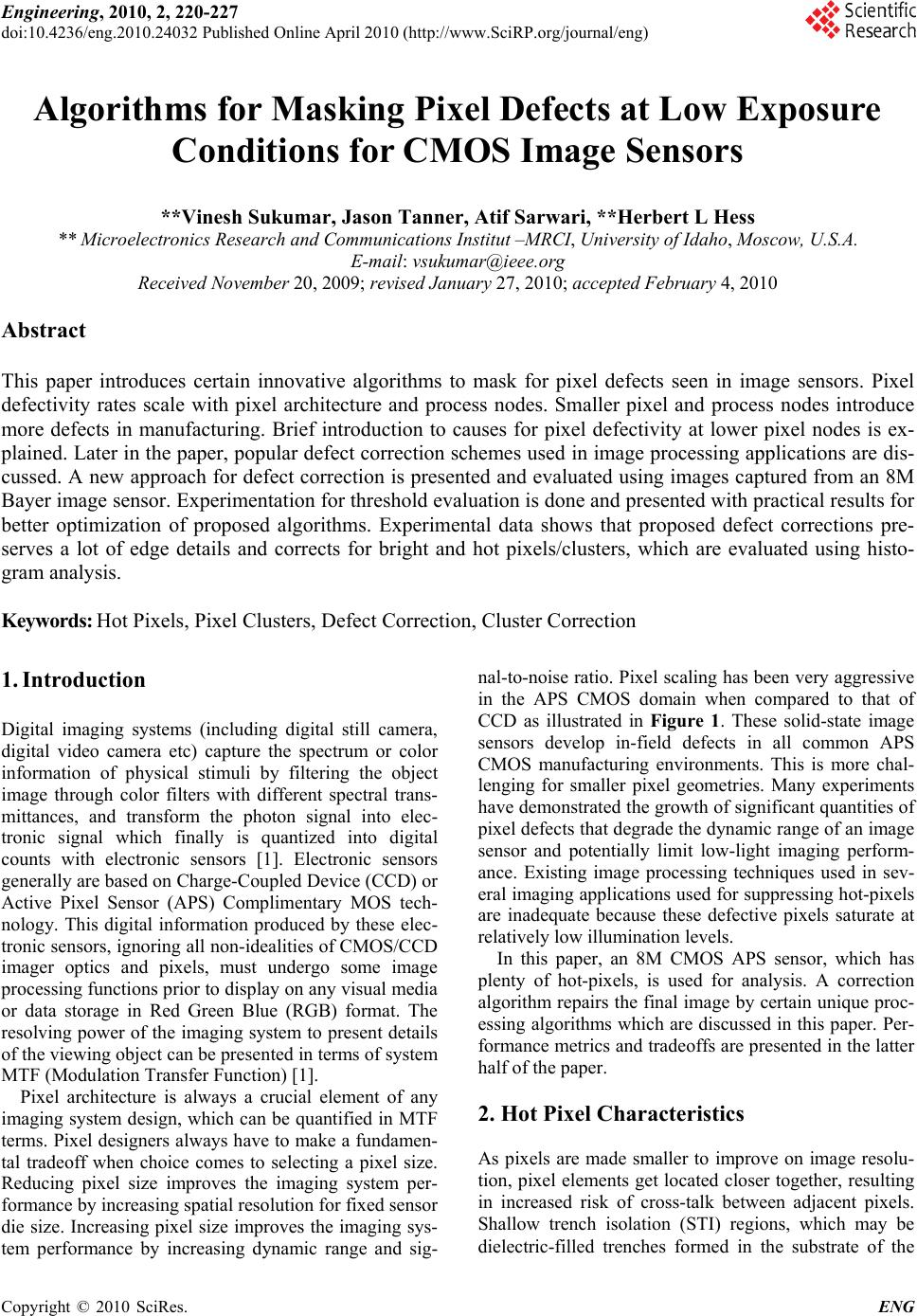 Engineering, 2010, 2, 220-227 doi:10.4236/eng.2010.24032 Published Online April 2010 (http://www.SciRP.org/journal/eng) Copyright © 2010 SciRes. ENG Algorithms for Masking Pixel Defects at Low Exposure Conditions for CMOS Image Sensors **Vinesh Sukumar, Jason Tanner, Atif Sarwari, **Herbert L Hess ** Microelectronics Resear ch and Communications Institut –MRCI, University of Idaho, Moscow, U.S.A. E-mail: vsukumar@ieee.org Received November 20, 2009; revised January 27, 2010; accepted Febr uary 4, 2010 Abstract This paper introduces certain innovative algorithms to mask for pixel defects seen in image sensors. Pixel defectivity rates scale with pixel architecture and process nodes. Smaller pixel and process nodes introduce more defects in manufacturing. Brief introduction to causes for pixel defectivity at lower pixel nodes is ex- plained. Later in the paper, popular defect correction schemes used in image processing applications are dis- cussed. A new approach for defect correction is presented and evaluated using images captured from an 8M Bayer image sensor. Experimentation for threshold evaluation is done and presented with practical results for better optimization of proposed algorithms. Experimental data shows that proposed defect corrections pre- serves a lot of edge details and corrects for bright and hot pixels/clusters, which are evaluated using histo- gram analysis. Keywords: Hot Pixels, Pixel Clusters, Defect Correction, Cluster Correction 1. Introduction Digital imaging systems (including digital still camera, digital video camera etc) capture the spectrum or color information of physical stimuli by filtering the object image through color filters with different spectral trans- mittances, and transform the photon signal into elec- tronic signal which finally is quantized into digital counts with electronic sensors [1]. Electronic sensors generally are based on Char ge-Cou pled Device (CCD) or Active Pixel Sensor (APS) Complimentary MOS tech- nology. This digital information produced by these elec- tronic sensors, ignoring all non-idealities of CMOS/CCD imager optics and pixels, must undergo some image processing functions prior to display on any visual media or data storage in Red Green Blue (RGB) format. The resolving power of the imaging system to present details of the viewing object can be presented in terms of system MTF (Modulat ion Transfer Functi o n ) [1] . Pixel architecture is always a crucial element of any imaging system design, which can be quantified in MTF terms. Pixel designers always have to make a fundamen- tal tradeoff when choice comes to selecting a pixel size. Reducing pixel size improves the imaging system per- formance by increasing spatial resolution for fixed sensor die size. Increasing pixel size improves the imaging sys- tem performance by increasing dynamic range and sig- nal-to-noise ratio. Pixel scaling has been very aggressive in the APS CMOS domain when compared to that of CCD as illustrated in Figure 1. These solid-state image sensors develop in-field defects in all common APS CMOS manufacturing environments. This is more chal- lenging for smaller pixel geometries. Many experiments have demonstrated the gro wth of significant quantities o f pixel defects that degrade the dynamic range of an image sensor and potentially limit low-light imaging perform- ance. Existing image processing techniques used in sev- eral imaging applications used for suppressing hot-pixels are inadequate because these defective pixels saturate at relatively low illumination levels. In this paper, an 8M CMOS APS sensor, which has plenty of hot-pixels, is used for analysis. A correction algorithm repairs the final image by certain unique proc- essing algorithms which are discussed in this paper. Per- formance metrics and tradeoffs are pr esented in the latter half of the paper . 2. Hot Pixel Characteristics As pixels are made smaller to improve on image resolu- tion, pixel elements get located closer together, resulting in increased risk of cross-talk between adjacent pixels. Shallow trench isolation (STI) regions, which may be dielectric-filled trenches formed in the substrate of the 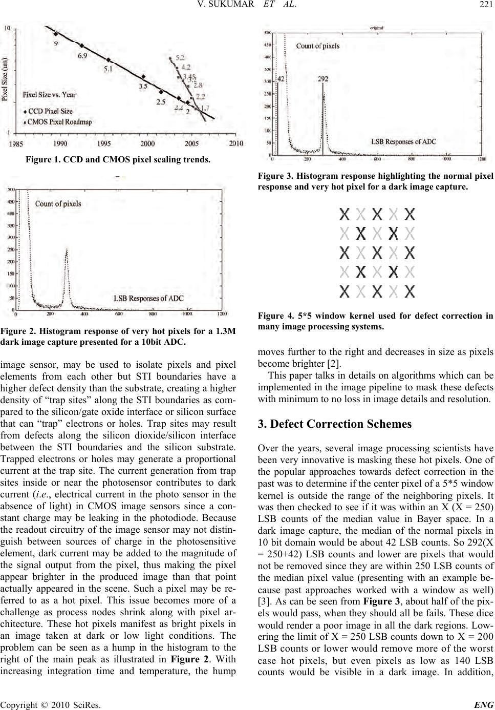 V. SUKUMAR ET AL. 221 Figure 1. CCD and CMOS pixel scaling trends. Figure 2. Histogram response of very hot pixels for a 1.3M dark image capture presented for a 10bit ADC. image sensor, may be used to isolate pixels and pixel elements from each other but STI boundaries have a higher defect density than the substrate, creating a higher density of “trap sites” along the STI boundaries as com- pared to the silicon/gate oxide in terface or silicon su rface that can “trap” electrons or holes. Trap sites may result from defects along the silicon dioxide/silicon interface between the STI boundaries and the silicon substrate. Trapped electrons or holes may generate a proportional current at the trap site. The current generation from trap sites inside or near the photosensor contributes to dark current (i.e., electrical current in the photo sensor in the absence of light) in CMOS image sensors since a con- stant charge may be leaking in the photodiode. Because the readout circuitry of the image sensor may not distin- guish between sources of charge in the photosensitive element, dark current may be added to the magnitude of the signal output from the pixel, thus making the pixel appear brighter in the produced image than that point actually appeared in the scene. Such a pixel may be re- ferred to as a hot pixel. This issue becomes more of a challenge as process nodes shrink along with pixel ar- chitecture. These hot pixels manifest as bright pixels in an image taken at dark or low light conditions. The problem can be seen as a hump in the histogram to the right of the main peak as illustrated in Figure 2. With increasing integration time and temperature, the hump Figure 3. Histogram response highlighting the normal pixel response and very hot pixel for a dark image capture. Figure 4. 5*5 window kernel used for defect correction in many image processing sy ste ms. moves further to the right and decreases in size as pixels become brighter [2]. This paper talks in details on algorithms which can be implemented in the image pipeline to mask these defects with minimum to no loss in image details and resolution. 3. Defect Correction Schemes Over the years, several image processing scientists have been very innovative is masking th ese hot pixels. One of the popular approaches towards defect correction in the past was to determine if the center pixel of a 5*5 window kernel is outside the range of the neighboring pixels. It was then checked to see if it was within an X (X = 250) LSB counts of the median value in Bayer space. In a dark image capture, the median of the normal pixels in 10 bit domain would be about 42 LSB counts. So 292(X = 250+42) LSB counts and lower are pixels that would not be removed since they are within 250 LSB counts of the median pixel value (presenting with an example be- cause past approaches worked with a window as well) [3]. As can be seen from Figure 3, about half of the pix- els would pass, when they should all be fails. These dice would render a poor image in all the dark regions. Low- ering the limit of X = 250 LSB counts down t o X = 2 0 0 LSB counts or lower would remove more of the worst case hot pixels, but even pixels as low as 140 LSB counts would be visible in a dark image. In addition, Copyright © 2010 SciRes. ENG 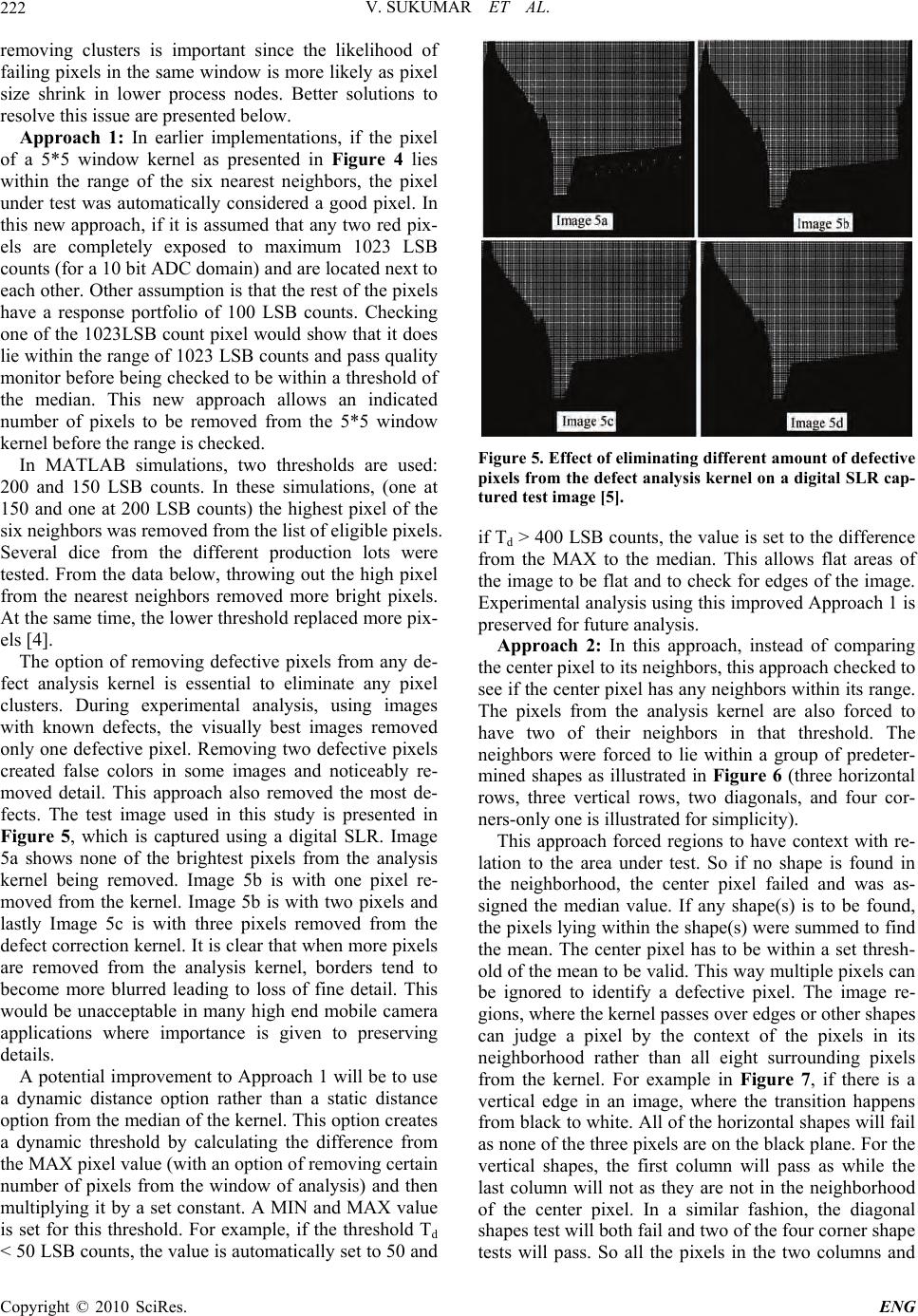 V. SUKUMAR ET AL. 222 removing clusters is important since the likelihood of failing pixels in the same window is more likely as pixel size shrink in lower process nodes. Better solutions to resolve this issue are presented below. Approach 1: In earlier implementations, if the pixel of a 5*5 window kernel as presented in Figure 4 lies within the range of the six nearest neighbors, the pixel under test was automatically considered a good pixel. In this new approach, if it is assumed that any two red pix- els are completely exposed to maximum 1023 LSB counts (for a 10 bit ADC domain) and are located nex t to each other. Other assumption is that the rest of the pixels have a response portfolio of 100 LSB counts. Checking one of the 1023LSB count pixel would show that it does lie within the range of 1023 LSB coun ts and pass quality monitor before being checked to be within a threshold of the median. This new approach allows an indicated number of pixels to be removed from the 5*5 window kernel before the range is checked. In MATLAB simulations, two thresholds are used: 200 and 150 LSB counts. In these simulations, (one at 150 and one at 200 LSB counts) the highest pixel of the six neighbors was removed from the list of eligible pixels. Several dice from the different production lots were tested. From the data below, throwing out the high pixel from the nearest neighbors removed more bright pixels. At the same time, the lower threshold replaced more pix- els [4]. The option of removing defective pixels from any de- fect analysis kernel is essential to eliminate any pixel clusters. During experimental analysis, using images with known defects, the visually best images removed only one defective pixel. Removing two defective pixels created false colors in some images and noticeably re- moved detail. This approach also removed the most de- fects. The test image used in this study is presented in Figure 5, which is captured using a digital SLR. Image 5a shows none of the brightest pixels from the analysis kernel being removed. Image 5b is with one pixel re- moved from the kernel. Image 5b is with two pixels and lastly Image 5c is with three pixels removed from the defect correction kernel. It is clear that when more pixels are removed from the analysis kernel, borders tend to become more blurred leading to loss of fine detail. This would be unacceptable in many high end mobile camera applications where importance is given to preserving details. A potential improvement to Approach 1 will be to use a dynamic distance option rather than a static distance option from the median of the kernel. This option creates a dynamic threshold by calculating the difference from the MAX pixel value (with an option of removing certain number of pixels from the window of analysis) and then multiplying it by a set constant. A MIN and MAX value is set for this threshold. For example, if the threshold Td < 50 LSB counts, the value is automatically set to 50 and Figure 5. Effect of eliminating different amount of defective pixels from the defect analysis kernel on a digital SLR cap- tured test image [5]. if Td > 400 LSB counts, the value is set to the difference from the MAX to the median. This allows flat areas of the image to be flat and to check for edges of the image. Experimental analysis using this improved Approach 1 is preserved fo r future analysis. Approach 2: In this approach, instead of comparing the center pixel to its neighb ors, this app ro ach ch eck ed to see if the center pixel has any neighbors within its range. The pixels from the analysis kernel are also forced to have two of their neighbors in that threshold. The neighbors were forced to lie within a group of predeter- mined shapes as illustrated in Figure 6 (three horizontal rows, three vertical rows, two diagonals, and four cor- ners-only one is illustrated for simplic ity). This approach forced regions to have context with re- lation to the area under test. So if no shape is found in the neighborhood, the center pixel failed and was as- signed the median value. If any shape(s) is to be found, the pixels lying with in the shape(s) were summed to find the mean. The center pixel has to be within a set thresh- old of the mean to be valid. This way multiple pixels can be ignored to identify a defective pixel. The image re- gions, where the kernel passes over edges or other shapes can judge a pixel by the context of the pixels in its neighborhood rather than all eight surrounding pixels from the kernel. For example in Figure 7, if there is a vertical edge in an image, where the transition happens from black to white. All of the horizontal shap es will fail as none of the thr ee pixe ls are on th e black plane . For the vertical shapes, the first column will pass as while the last column will not as they are not in the neighborhood of the center pixel. In a similar fashion, the diagonal shapes test will both fail and two of the four corner shap e tests will pass. So all the pixels in the two columns and Copyright © 2010 SciRes. ENG 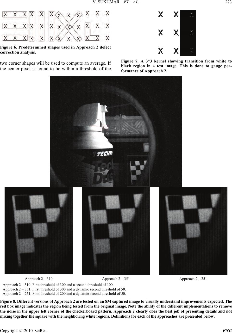 V. SUKUMAR ET AL. Copyright © 2010 SciRes. ENG 223 Figure 6. Predetermined shapes used in Approach 2 defect correction analysis. Figure 7. A 3*3 kernel showing transition from white to black region in a test image. This is done to gauge per- formance of Approach 2. two corner shapes will be u sed to compute an average. If the center pixel is found to lie within a threshold of the Approach 2 – 310 Approach 2 – 351 Approach 2 – 251 Approach 2 – 310: First th reshold of 300 and a second thres hol d o f 100. Approach 2 – 351: First th reshold of 300 and a dynam ic second threshold of 50. Approach 2 – 251: First th reshold of 200 and a dynam ic second threshold of 50. Figure 8. Different versions of Approach 2 are tested on an 8M captured image to visually understand improvements expected. The red box image indicates the region being tested from the original image. Note the ability of the different implementations to remove the noise in the upper left corner of the checkerboard pattern. Approach 2 clearly does the best job of presenting details and not mixing together the square with the neighboring white regions. Definitions for each of the approaches are presented below. 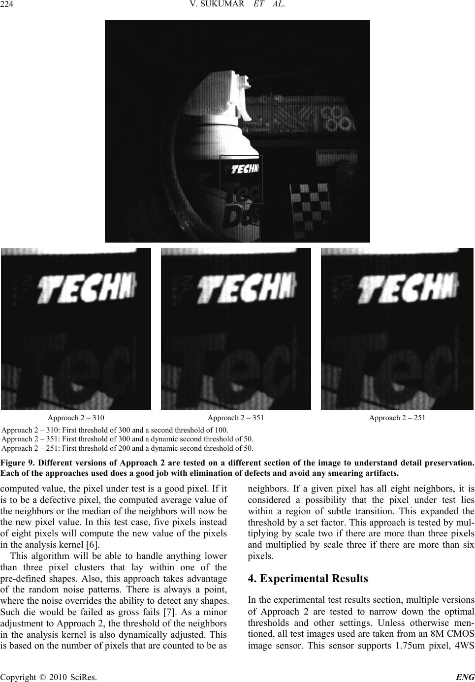 V. SUKUMAR ET AL. 224 Approach 2 – 310 Approach 2 – 351 Approach 2 – 251 Approach 2 – 310: First th reshold of 300 and a second thres hol d o f 100. Approach 2 – 351: First th reshold of 300 and a dynam ic second threshold of 50. Approach 2 – 251: First th reshold of 200 and a dynam ic second threshold of 50. Figure 9. Different versions of Approach 2 are tested on a different section of the image to understand detail preservation. ach of the approaches used does a good job with elimination of defects and avoid any smearing artifacts. E computed value, the pixel und er test is a good pixel. If it is to be a defectiv e pixel, the computed average value of the neighbors o r the median o f the n eighb ors will now b e the new pixel value. In this test case, five pixels instead of eight pixels will compute the new value of the pixels in the analysis kernel [6 ]. This algorithm will be able to handle anything lower than three pixel clusters that lay within one of the pre-defined shapes. Also, this approach takes advantage of the random noise patterns. There is always a point, where the noise overrides the ability to d etect any shapes. Such die would be failed as gross fails [7]. As a minor adjustment to Approach 2, the threshold of the neighbors in the analysis kernel is also dynamically adjusted. This is based on the number of pixels that are coun ted to be as neighbors. If a given pixel has all eight neighbors, it is considered a possibility that the pixel under test lies within a region of subtle transition. This expanded the threshold by a set factor. This approach is tested by mul- tiplying by scale two if there are more than three pixels and multiplied by scale three if there are more than six pixels. 4. Experimental Results In the experimental test results section, multiple versions of Approach 2 are tested to narrow down the optimal thresholds and other settings. Unless otherwise men- tioned, all test images used are taken from an 8M CMOS image sensor. This sensor supports 1.75um pixel, 4WS Copyright © 2010 SciRes. ENG 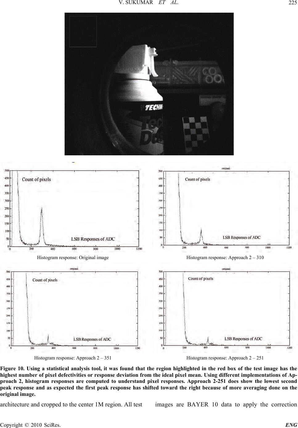 V. SUKUMAR ET AL. 225 Histogram response: Original imag e Histogram response: Appr oach 2 – 310 Histogram response: Appr oach 2 – 351 Histogram response: Appr oach 2 – 251 Figure 10. Using a statistical analysis tool, it was found that the region highlighted in the red box of the test image has the highest number of pixel defectivities or response deviation from the ideal pixel mean. Using different implementations of Ap- proach 2, histogram responses are computed to understand pixel responses. Approach 2-251 does show the lowest second peak response and as expected the first peak response has shifted toward the right because of more averaging done on the riginal image. o architecture and cropped to the center 1M region. All test images are BAYER 10 data to apply the correction Copyright © 2010 SciRes. ENG 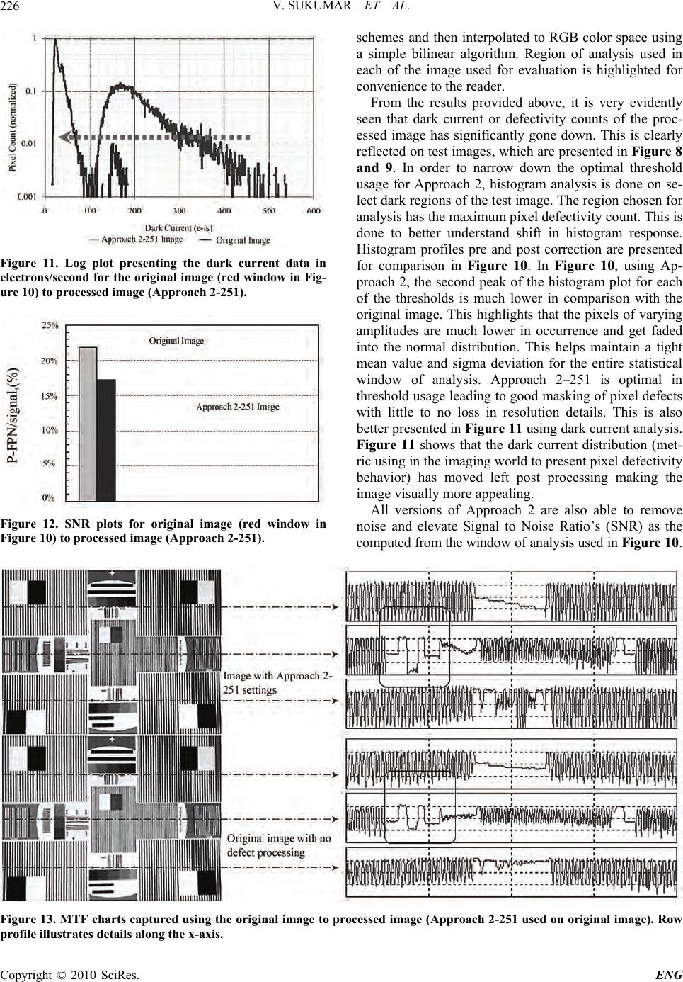 V. SUKUMAR ET AL. 226 Figure 11. Log plot presenting the dark current data in electrons/second for the original image (red window in Fig- ure 10) to processed image (Approach 2-251). Figure 12. SNR plots for original image (red window in Figure 10) to processed image (Approach 2-251). schemes and then interpolated to RGB color space using a simple bilinear algorithm. Region of analysis used in each of the image used for evaluation is highlighted for convenience to the reader. From the results provided above, it is very evidently seen that dark current or defectivity counts of the proc- essed image has significantly gone down. This is clearly reflected on test images, which are presented in Figure 8 and 9. In order to narrow down the optimal threshold usage for Approach 2, histogram analysis is done on se- lect dark regions of the test image. The region chosen for analysis has the maximum pixel defectivity count. This is done to better understand shift in histogram response. Histogram profiles pre and post correction are presented for comparison in Figure 10. In Figure 10, using Ap- proach 2, the second peak of the histogram plot for each of the thresholds is much lower in comparison with the original image. This highlights that the pixels of varying amplitudes are much lower in occurrence and get faded into the normal distribution. This helps maintain a tight mean value and sigma deviation for the entire statistical window of analysis. Approach 2–251 is optimal in threshold usage leading to good masking of pixel defects with little to no loss in resolution details. This is also better presented in Figure 11 using dark current analysis. Figure 11 shows that the dark current distribution (met- ric using in the imaging world to present pixel defectivity behavior) has moved left post processing making the image visually more appealing. All versions of Approach 2 are also able to remove noise and elevate Signal to Noise Ratio’s (SNR) as the computed from the window of analysis used in Figure 10 . Figure 13. MTF charts captured using the original image to processed image (Approach 2-251 used on original image). Row profile illustrates details along the x-axis. Copyright © 2010 SciRes. ENG 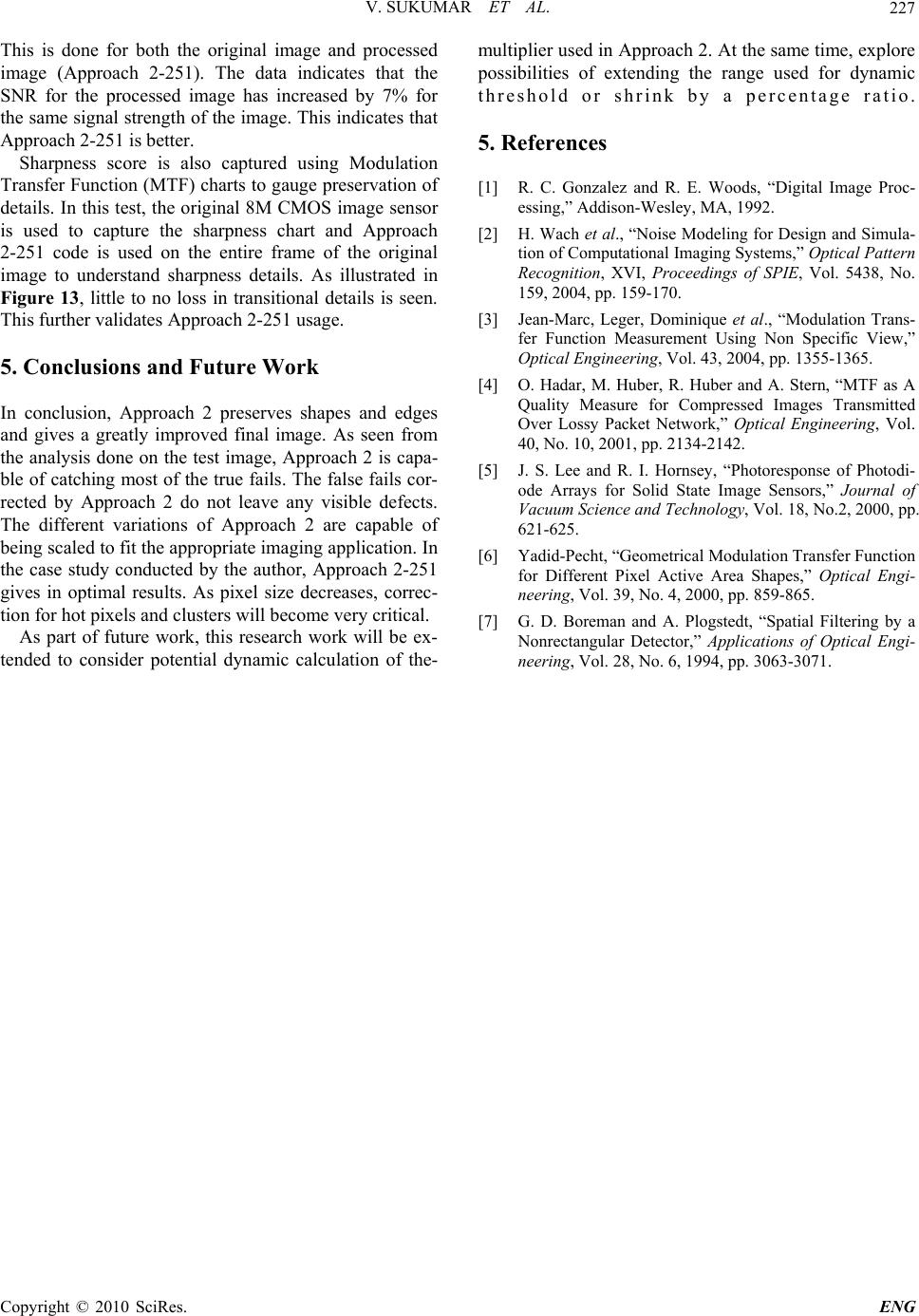 V. SUKUMAR ET AL. 227 This is done for both the original image and processed image (Approach 2-251). The data indicates that the SNR for the processed image has increased by 7% for the same signal strength of the image. This indicates that Approach 2- 2 5 1 is bet t e r. Sharpness score is also captured using Modulation Transfer Function (MTF) charts to gauge preservation of details. In this test, the original 8M CMOS image sensor is used to capture the sharpness chart and Approach 2-251 code is used on the entire frame of the original image to understand sharpness details. As illustrated in Figure 13, little to no loss in transitional details is seen. This further validates Approa ch 2- 2 51 usa ge . 5. Conclusions and Future Work In conclusion, Approach 2 preserves shapes and edges and gives a greatly improved final image. As seen from the analysis done on the test image, Approach 2 is capa- ble of catching most of the true fails. The false fails cor- rected by Approach 2 do not leave any visible defects. The different variations of Approach 2 are capable of being scaled to fit the ap propriate imagin g app lication . In the case study conducted by the author, Approach 2-251 gives in optimal results. As pixel size decreases, correc- tion for hot pixels and clusters will become very critical. As part of future work, this research work will be ex- tended to consider potential dynamic calculation of the- multiplier used in Approach 2. At the same time, explore possibilities of extending the range used for dynamic threshold or shrink by a percentage ratio. 5 . References [1] R. C. Gonzalez and R. E. Woods, “Digital Image Proc- essing,” Addison-Wesley, MA, 1992. [2] H. Wach et al., “Noise Modeling for Design and Simula- tion of Computational Imaging Systems,” Optical Patte rn Recognition, XVI, Proceedings of SPIE, Vol. 5438, No. 159, 2004, pp. 159-170. [3] Jean-Marc, Leger, Dominique et al., “Modulation Trans- fer Function Measurement Using Non Specific View,” Optical Engineering, Vol. 43, 2004, pp. 1355-1365. [4] O. Hadar, M. Huber, R. Huber and A. Stern, “MTF as A Quality Measure for Compressed Images Transmitted Over Lossy Packet Network,” Optical Engineering, Vol. 40, No. 10, 2001, pp. 2134-2142. [5] J. S. Lee and R. I. Hornsey, “Photoresponse of Photodi- ode Arrays for Solid State Image Sensors,” Journal of Vacuum Science and Technology, Vol. 18, No.2, 2000, pp. 621-625. [6] Yadid-Pecht, “Geometrical Modulation Transfer Function for Different Pixel Active Area Shapes,” Optical Engi- neering, Vol. 39, No. 4, 2000, pp. 859-865. [7] G. D. Boreman and A. Plogstedt, “Spatial Filtering by a Nonrectangular Detector,” Applications of Optical Engi- neering, Vol. 28, No. 6, 1994, pp. 3063-3071. Copyright © 2010 SciRes. ENG |