Journal of Modern Physics
Vol.2 No.12(2011), Article ID:16507,7 pages DOI:10.4236/jmp.2011.212191
Study of “Radiation Effects of Nuclear High Energy Particles” on Electronic Circuits and Methods to Reduce Its Destructive Effects
Islamic Azad University, Dashtestan Branch, Borazjan, Iran
E-mail: *mastidarush@yahoo.com
Received September 13, 2011; revised November 3, 2011; accepted November 27, 2011
Keywords: Electronic circuits, radiation, silicon, high energy neutrons, simulated, thermal
ABSTRACT
This research concerns on (TID), (DD) and (SEE) effects also high energy particles’ effects on electronic properties of silicon. It investigates the silicon electronic properties exposed to these particles using a laboratory neutron radiation sources. Some Pieces of a silicon wafer were under neutron radiation at different times and the electrical properties of each one was illustrated by plate resistance measurement and also the strength of the current voltage was simulated by Fluka and MCNP software. Based on these results, authorized limit of silicon tolerance was obtained against high energy neutrons radiation. We put them in the electric furnace under thermal recovery to overcome the unusual behavior of irradiated samples.
1. Introduction
By expanding the field of human space and nuclear energy exploration technologies, there are a huge demands on semiconductor components in the nuclear radiation environments. The pieces are used in different parts of spacecraft and nuclear plants. High energy particles such as electrons, protons and neutrons are some other kinds of radiation in nuclear environments [1]. Ionizing radiations emitted from radiation sources are the main part of space radiation environment and nuclear sites, the prevalence of abnormalities on electronic systems and communications satellites and nuclear power plants [2]. For example, the nuclear reactor parameters and pressure, temperature and neutron flux transducers are measured by sensors which the sensors and transducers are used in the electronics circuits and these devices are energetic particles and radiation in the environment. The nuclear radiation has some effects on various electronic circuits and telecommunications, particularly the effects of total ionizing dose (TID) and single event effects (SEE) [3].
2. Theory and Background
Ionizing radiations are the radiations which in collision with atoms, have enough energy to separate the electrons orbiting atoms and charged or ionized atoms. High energy ionized particles such as protons, heavy ions and electrons influence on electronic systems. These effects can decrease the efficiency and performance of the system or off the device. So the equipments may face a short lifespan or defect and a huge disadvantage [1]. In reducing the amount of obtained energy of the electronic components a shield can be used [4]. But this method cannot counter single event effects and total ionization forced by high energy ionized particles, so it may cause some defects and probable errors in each part [5]. Semiconductors are the main structure of the electronic components. Semiconductor devices properties after exposure to radiation are so important they the behavior and lifetime of these parts can be predicted, because radiation creates irreversible damage [6]. In this study, it is necessary to provide high energy particle radiation conditions in the laboratory environment. The laboratory neutron radiation sources were used. Neutrons are preferred because; high energy radiation from other particles can also be simulated by it. Creation of crystal defects in semiconductors is mainly due to the improper position of atoms within the network instead of ordinary position. The fast neutrons can be localized cluster like defects in the material, during manufacturing penetrating to other areas and therefore leading to the breakdown of voltage and changing the device leakage current. Irradiating the crystal with high energy neutrons, results a wide range of defects. Such shortcomings have elliptical or nearly spherical shape. Frnkly couples are the simplest defects resulted by fast neutrons. The numbers of Frnkly couples formed per a fast neutron are estimated by KINE CHIN PICE model according to the following relation [5]:
 (1)
(1)
where
3. Laboratory Activities
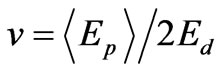
The silicon wafer of n (100) type was cut to the sample sizes of 1 cm × 2 cm × 0.7 mm and after the cleaning and cutting; four-point probe resistivity of the samples was measured. To ensure repeatability, every step of the experiment was carried out by a number of, samples and the resistance test of each sample was done in several different spots, and almost the same results were obtained in each group. The measurement result of a sample before irradiation is shown in Figure 1. As it can be seen in the figure, the current changes in the amount of impedance (resistance plate) in the range of 450 - 1800 ohms.
The samples were then irradiated. This experiment was done by using a neutron beam with flux control features Φ1 = 2.8 × 10¹⁵ n·cm−2 and the value j = 2 × 10⁸ n·cm−2·s−1 the samples also had different radiation times at first. In this study, neutron irradiation can be divided into three categories according to their energy as follows: 1) Fast neutrons with energies greater than 10 Kev. 2) Intermediate neutrons (Epithermal) energy of less than 10 Kev and more than 1 ev. 3) Thermal neutrons with energy less than 1 ev.
Fast neutrons have small absorption cross section, it means that the absorption of these neutrons by these elements is little and mainly these neutrons destruct the crystalline semiconductors and cause different defects. Intermediate neutrons make point defects [5]. For better understanding the radiation process, the relative flux of
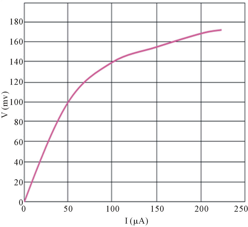
Figure 1. Characteristic of voltage—instance current of group A before the neutron irradiation.
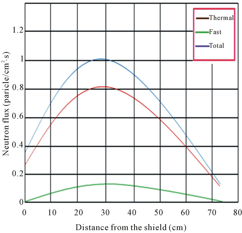
neutrons were estimated in the chamber for three energies above using the MCNP and Fluka software [7,8]. Considering a sample in shield changes neutrons distribution so it was simulated with and without the sample. Estimation result of a sample is shown in Figure 2. The samples with very low absorption cross section of semiconductors virtually have “no effect on the chart”.
In this study, five samples were selected for irradiation characteristics based on the rate and duration of radiation exposure in accordance with Table 1. These values are calculated based on the MCNP software [8]. The lowest dose of E was seen close to the neutron source and has fast neutron flow.
After irradiation, the samples were taken away from the neutron source and after elapsing at least 10 times the half life decay, the activity levels were measured at first. After making sure they are not radioactive, resistivity and voltage-current characteristics of them were measured and plotted again in the new conditions. The four probe device was used to measure resistivity. The results of a four-point probe method for measuring the voltage in terms of current on the sample A, after irradiation are plotted in Figure 3. Measurements were repeated several times and in different environments and nearly the same results were obtained. Based on the characteristics, voltage-current relationship was not as previous. Secondly, the average resistance value is about two mega-ohms about 4000 times larger than the amount of measured resistance before radiation.
The increase of ohmic resistance of the sample is the reason of the disassemble in the crystal lattice, and its defects. In order to overcome the unusual behavior of irradiated samples, we put them in the electric furnace
 (a)
(a) (b)
(b)
Figure 2. Simulation of the neutron flux distribution in the shield using the software in the case of FLUKA in compartment (a) and (b) in no compartment.
with a temperature of 380˚C for 10 hours under Thermal (thermal recovery) [9]. Due to the presence of defects in the samples, all of them needed thermal recovery. Intermediate neutrons cause point defects which are resolved by thermal recovery at temperatures of about 400˚C. By thermal treatment some voltage-current defects were removed and less radiation in samples returns impedance amount to the amount before radiation. For example, Sample characteristic of thermal treatment is shown in Figure 4. In order to remove defects the temperature of
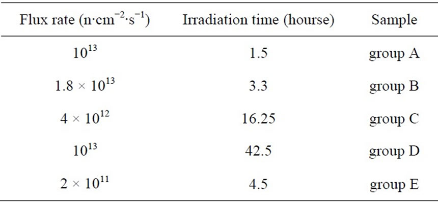
Table 1. characteristics of irradiation samples.
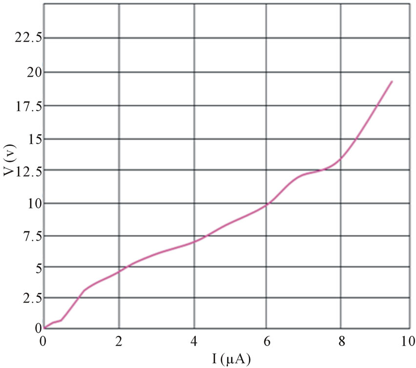
Figure 3. Typical voltage-current characteristics of group A after neutron irradiation.
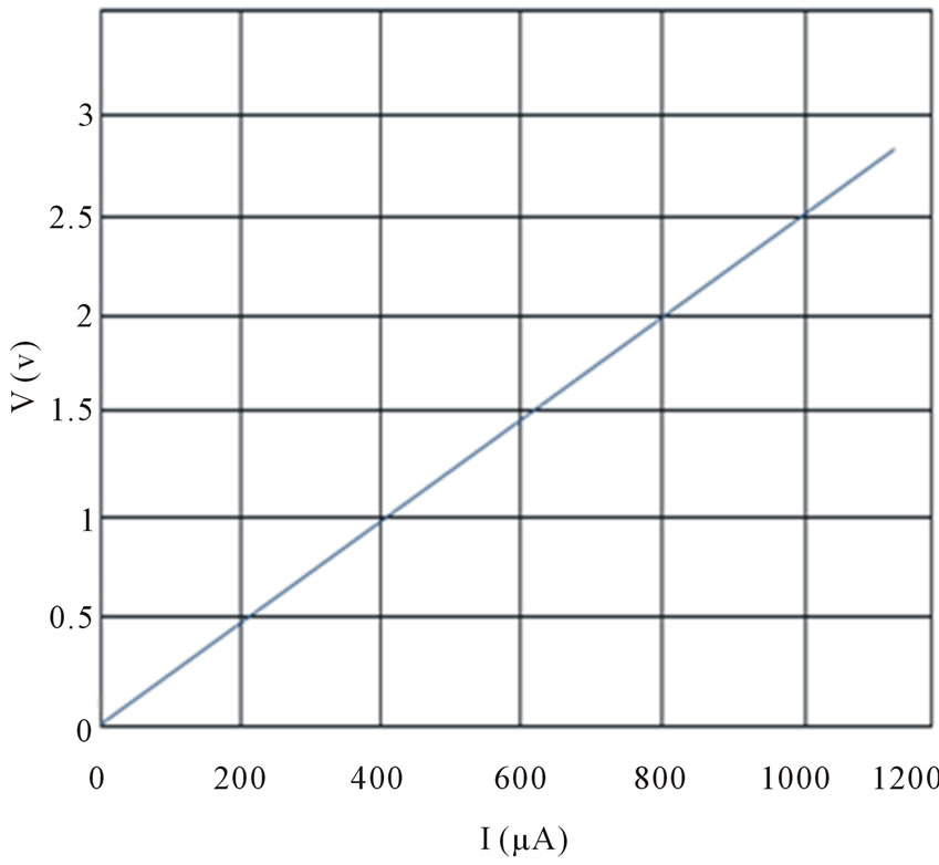
Figure 4. Typical voltage-current characteristics of group A after neutron irradiation and thermal recovery.
400˚C for thermal neutrons, and 750˚C for fast neutrons, was necessary to eliminate fast neutrons defects after thermal recovery.
The results of measuring the voltage were obtained in terms of current on the four point probe method for samples A, C, D, E after irradiation (results after thermal recovery), the graph of Figure 5 respectively. As it is observed only sample A is returned back to original state and other samples have significant changes in their resistance.
4. Simulation of Radiation High Energy Particless’ Environment
Energetic ionized particles are classified into three categories [10]: Space belts—Consisting particles such as electrons (to the extent of 30 Mev), protons (to 200Mev), inner belt (450 to 3500 km altitude), and the outer Van Allen belt (8500 to 16,000 km altitude). Spectrum of electrons (500 ev - 20 Mev) in this area for nuclear environment by Fluka software is simulated and calculated [7] and the rate of high energy protons and electrons beam energy, are shown in figures 6 and 7. The high energy protons or electrons produce the network defects in semiconductors crystalline and cause displacement damage [5].
5. Radiation Effects on Electronics
The nuclear radiation effects are divided into two categories: Cumulative effects and single event effects (SEE). Negative and destructive effects on the electronic components are because of protons and electrons and heavy ions and result to unusual behavior in most electronics [11].
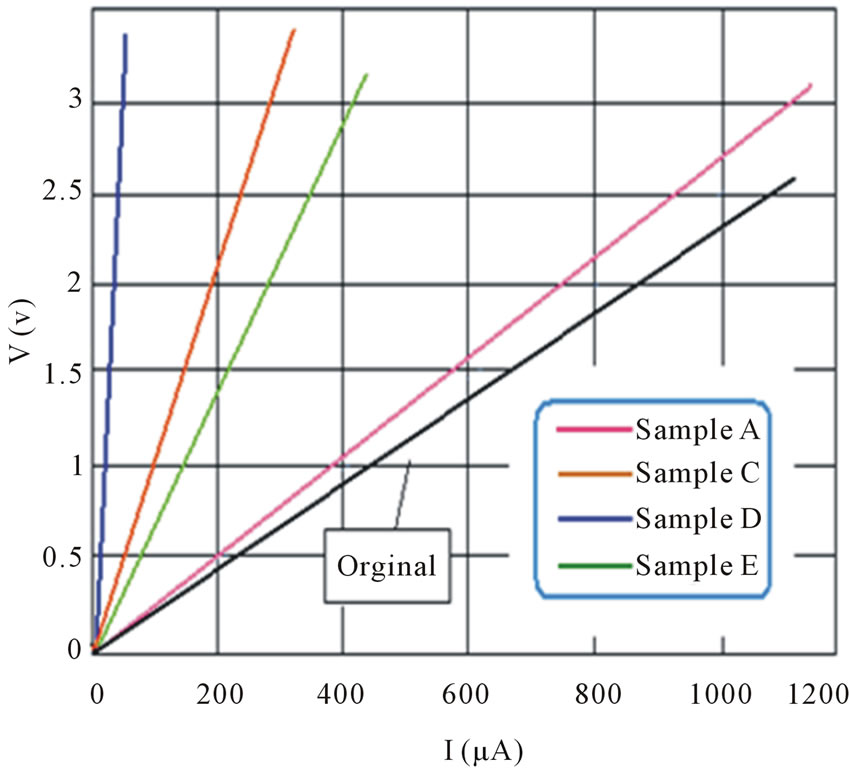
Figure 5. Drawing graphs in a coordinate system in a logarithmic scale to the thermal recovery.
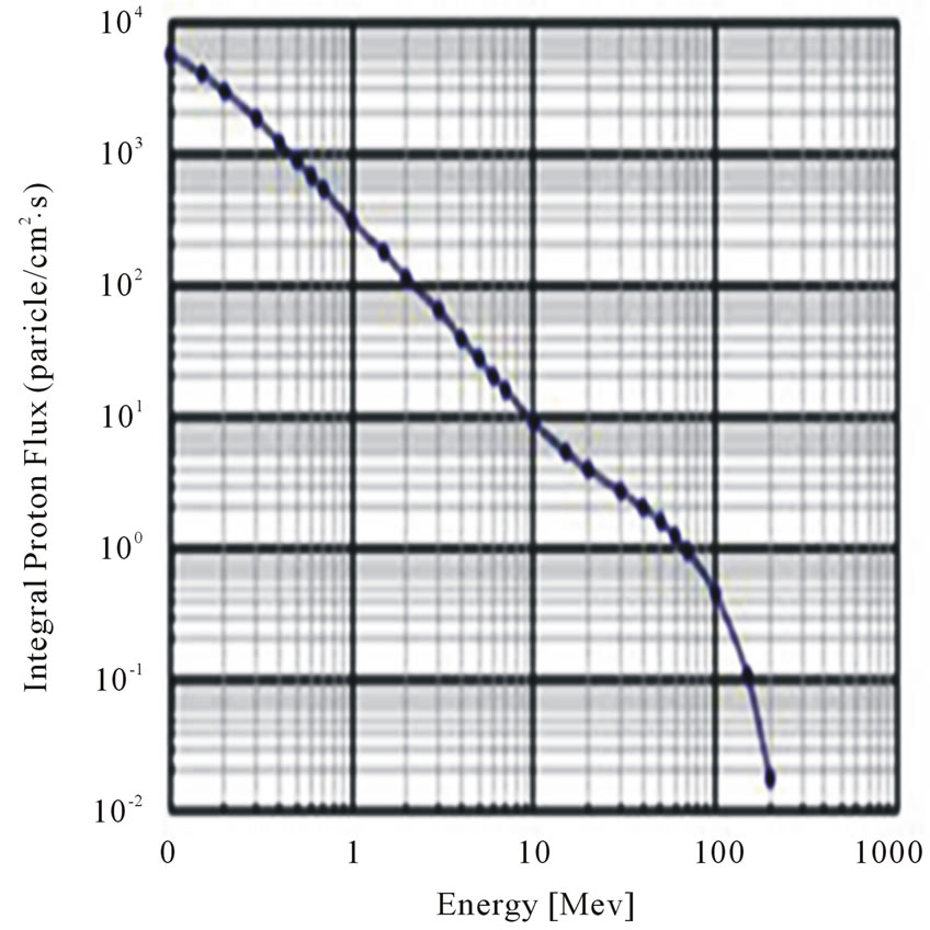
Figure 6. The energy spectrum of trapped protons and electrons, for the calculation of solar proton spectra [1], the Fluka software was used.
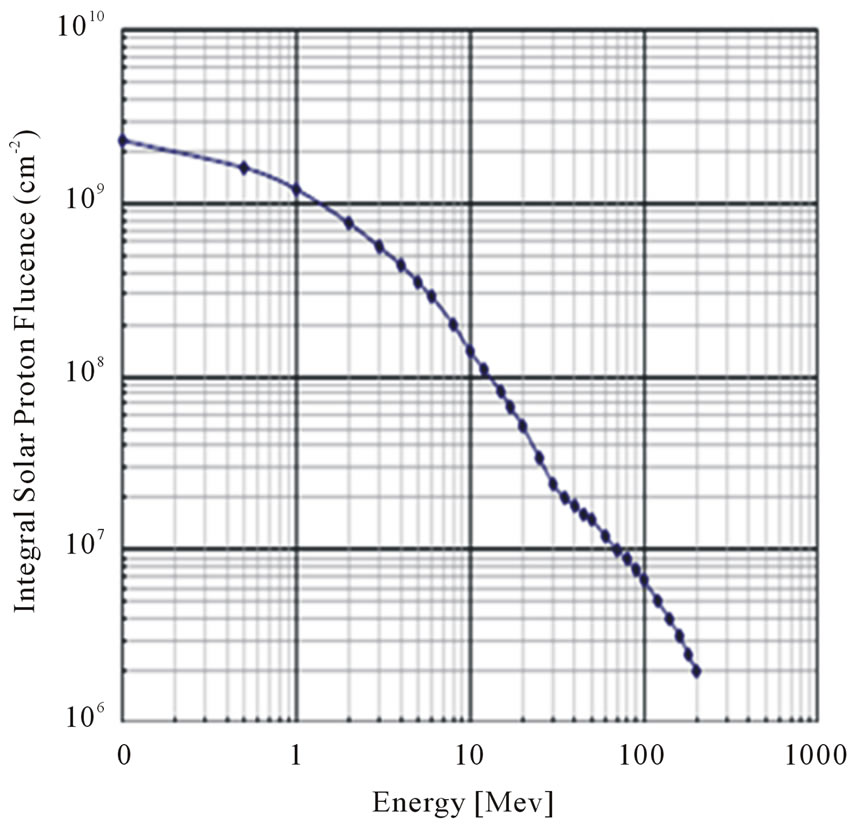
Figure 7. The energy spectrum of the high energy protons.
5.1. Cumulative Effects
These effects are derived from the production or activation of microscopic defects in electronic components semiconductors. Cumulative effects are classified in two parts: Total ionization dose (TID) and displacement damage (DD). When a high energy particle collides with mater, there are two major phenomenons [12]: 1) Ionization phenomenon, which is the interaction of particles with the atomic shell electrons. This phenomenon causes hole-electron pairs. Electrons come out due to the greater freedom of movement, and holes trap in the border SiO2 as the conductors in electronics assembly are and can eventually cause a change in the electrical specifications. 2) Interaction with the nucleus of an atom by transferring enough energy the atom displacement. Indeed, high energy protons or electrons result in network defects in semiconductors and, leading to the production and displacement damage (DD).
5.1.1. Total Ionization Dose Effects (TID)
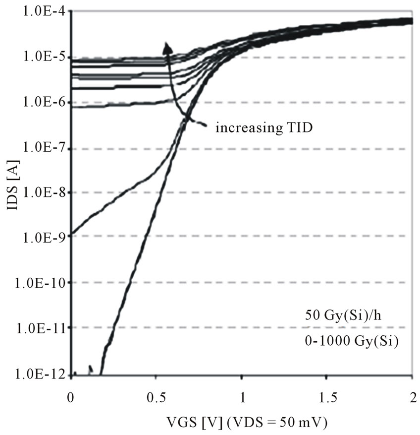
TID results in the change or loss of parameters of electronic piece such as leakage current, threshold voltage shift, and in semiconductors, it produces the electron hole -pairs in the dielectric layers and the secondary particles [13]. Active and high energy ions can damage materials by breaking or rearranging atomic bands. In general, electrical and electronic components, a lot of materials such as insulation and dielectric capacitors, insulators cables and circuit board materials, may lead to the reduction of the insulation or electrical leakage after enough exposure to total ionization radiation. Similarly conductor materials, such as the resistance of metal plates, the TID radiation exposure can be changed or charged by exposing TID radiation. Nowadays, the most effective element influenced by the nuclear radiation in electronic circuits and telecommunications is a MOSFET transistor. Gate oxide, an ideal insulator is made of a silicon dioxide. There is a problem when the piece is exposed to radiation. First the gate oxide is ionized by absorbed dose, and free electrons and holes movement are influenced by electric field caused by the gate voltage, in oxide. The electrons are safe if they go out the oxide and disappear. But except electrons, a small fraction of holes trap in the gate and change the parameter [3]. By creating energy (TID), the piece will be turned on even if the voltage is not controlled. As a result, gate doesn’t control the drain-source transistor the piece will remain on. PMOS transistors and operate similar but in a different direction. When the radiated ray traps enough positive charge in the gate oxide, the transistor remains off [14]. Moreover charge storage influences, the characteristic of voltage-current transistors (Figures 8 and 9). Threshold voltage moves by exposing transistors to radiations and enough dose storage (figure 8) and it increases the leakage current, so power consumption increases and the chip is defected (Figure 9(b)). Moreover, the on and off position of the transistor cannot be controlled anymore [6].
One of the methods of decreasing these effects is to reduce the gate oxide layer. So thinner gate oxide, results in trapping less positive charge and CMOS transistors become more resistant against radiation. By decreasing transistors sizes, they also receive lower dose and have
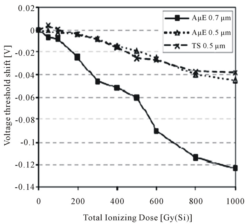
Figure 8.Threshold voltage shift.
less parameter changes. TID effects will be decreased by putting transistors inside the covered chamber and shielding electronic circuits [4].
The shield effect on the charged particles in the nuclear radiation is using MCNP and Fluka software shown in figure 10 [7,8].
5.1.2. Displacement Damage Effect (DD)
The first known resources causing DD are protons and radio isotopes producing neutrons. When high energy proton and neutron particles influence inside a semiconductor crystal network like silicon, there are several mechanisms to move atoms. Elastic scattering is an example. Some of the particles can transfer energy to the silicon core in this phenomenon. If enough energy transfers (almost 25 ev) the core exits of its location [6]. Released silicon atom, can lose its energy by ionization changing location by the other atoms. For example in a JFET transistor, it is exposed to neutrons or protons and new recombination’s centers are created. So electron recombination with holes in the base will probably be increased and by increasing the flux of neutrons or protons, it reduces transistor gain [12]. Some charges scattered in displacement damage, reduces the transistor conductivity and increase, the noise level. Displacement damage effects cause the tunneling phenomenon, increasing the current, bias change and the electrical field change in the semiconductor segment.
5.2. Single Event Effects (SEE)
The energy of ion loses in its path within the semiconductor device, creates the intense current with a maximum peak of several hundred micro-amps in a short time (less
 (a)
(a) (b)
(b)
Figure 9. (a) The curve of current-voltage changes; (b) leakage current creation.
than 9 ns) at the electrical nodes. This unwanted current leads to stable disturbances. Also single event effects transient disturbance damage cause instantaneous changes in the analog signals [11]. SEE effects are stable disorder which result to the moment changes in digital signals and it just damages the data [12].The dielectric charge is the other effect. The radiation sources cause this, so electrons enter the domestic environment of spacecraft nuclear
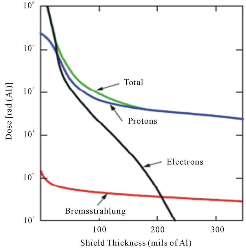
Figure 10. The shield effect on the TID.
equipment and it results the accumulation of charge in electric insulators, cable sheathing, electronic boards and electrical fittings. Charging and discharging electrons also causes breakdown voltage in components. in addition to shielding for countering the single event effects it is necessary to have the various circuit techniques to reduce single event effects as well [5]. Smalling circuit dimensions and reducing the transistors size leads to reducing charges which single event effect creates in circuit elements. In addition, circuit techniques, “vote logic” can be used. It is used to correct potential errors in latches. The latch cannot change a bit position by itself in this technique, but some similar latches are required. This situation will only be changed when the majority latches want to exit. So the other latches identify and eliminate a lonely latch error. Other circuit techniques are used, such as “error detection and correction” in addition to shield and reduction of the transistors sizes in order to reduce single event effects in logic circuits [4].
6. Conclusions
According to calculations, simulations and experimental work done and the results of the investigation it was determined that nuclear radiations have effects, such as the creation of defects in segment, and behavioral characteristic change and creating leakage currents and noise. Total ionization dose rate effects (TID) and single event effects (SEE) mostly limit performance of electronic equipment and telecommunications. There are some methods to counter these effects such as shielding, reducing the transistor sizes, circuit dimensions and various circuit techniques. Also in laboratory, the effects of neutron irradiation on the electronic properties of silicon were investigated and it has been shown that a high energy particle such as neutrons has a significant effect on electronic properties of semiconductor devices. The influence was displayed as of crystal defects decreasing the conductance and increasing resistance. The thermal recovery operation was performed to repair damages and it was observed that the samples which were too near the sources of radiation or under a long time radiation can be recovered with the higher temperature (750˚C).
REFERENCES
- L. W. Townsend, J. L. Shinn and J. W. Wilson, “Interplanetary Crew Exposure Estimates for the August 1972 and October 1989 Solar Particle Events,” Radiation Research, Vol. 126, No. 1, 1991, pp. 108-110. doi;10.2307/3578178
- F. A. Cucinotta, W. Schimmerling, J. W. Wilson, L. E. Petersen, G. D. Badhwar, P. B. Saganti and J. F. Dicello, “Space Radiation Cancer Risk Projections for Exploration Missions: Uncertainty Reduction and Mitigation,” DIANE Publishing, Darby, 2001.
- T. Liu, “Total Ionization Dose Effects and Single-Event Effects Studies of a 0.25 μm Silicon-on-Sapphire CMOS Technology,” 9th European Conference on Radiation and Its Effects on Components and Systems, Deauville, 10-14 September 2007, pp. 1-5.
- E. N. Parker, “Shielding Astronauts from Cosmic Rays,” Space Weather, Vol. 3, 2005, p. S08004.
- A. H. Johnston, “Radiation Damage of Electronic and Optoelectronic Devices in Space,” 4th International Workshop on Radiation Effects on Semiconductor Devices for Space Application, Tsukuba, 11-13 October 2000.
- G. C. Messenger and M. S. Ash, “The Effects of Radiation on Electronic Systems,” Van Nostrand Reinhold, New York, 1992.
- A. Ferrari, et al., “Fluka: A Multi-Particle Transport Code,” CERN, Geneva, 2005.
- X-5 Monte Carlo Team, “MCNP-A General Monte Carlo N-Particle Transport Code,” Los Alamos National Laboratory, Los Alamos, 2003.
- T. P. Ma and P. V. Dressendorfer, “Ionizing Radiation Effects in MOS Devices and Circuits,” John Wiley and Sons, New York, 1989.
- S. Duzellier, “Radiation Effects on Electronic Devices in Space,” Aerospace Science and Technology, Vol. 9, No. 1, 2005, pp. 93-99. doi;10.1016/j.ast.2004.08.006
- G. C. Messenger and M. S. Ash, “Single Event Phenomena,” Kluwer Academic Publishers, New York, 1997. doi;10.1007/978-1-4615-6043-2
- G. Barbottin and A. Vapaille, “Instabilities in Silicon Devices,” Elsevier, Berlin, 1999.
- H. J. Barnaby, M. Mclain and I. S. Esqueda, “Total-IonIzing-Dose Effects on Isolation Oxides in Modern CMOS Technologies,” Nuclear Instruments and Methods in Physics Research B, Vol. 261, No. 1-2, 2007, pp 1142-1145. doi;10.1016/j.nimb.2007.03.109
- H. J. Barnaby, “Total-Ionizing-Dose Effects in Modern CMOS Technologies,” IEEE Transactions on Nuclear Science, Vol. 53, No. 6, 2006, pp. 3103-3121. doi;10.1109/TNS.2006.885952