Vol.2, No.3, 197-200 (2010) Natural Science
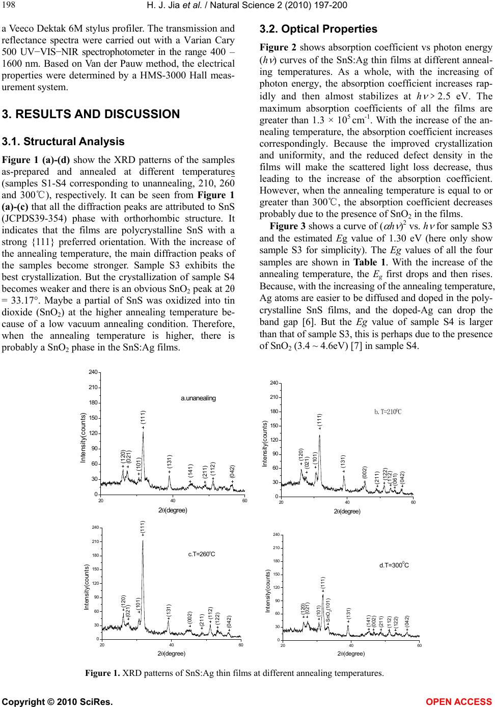
http://dx.doi.org/10.4236/ns.2010.23030
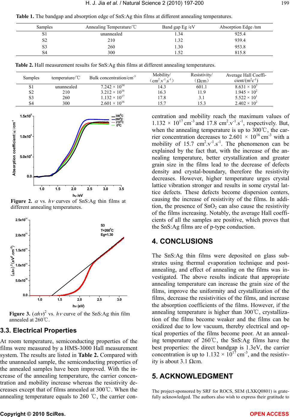
Copyright © 2010 SciRes. OPEN ACCESS
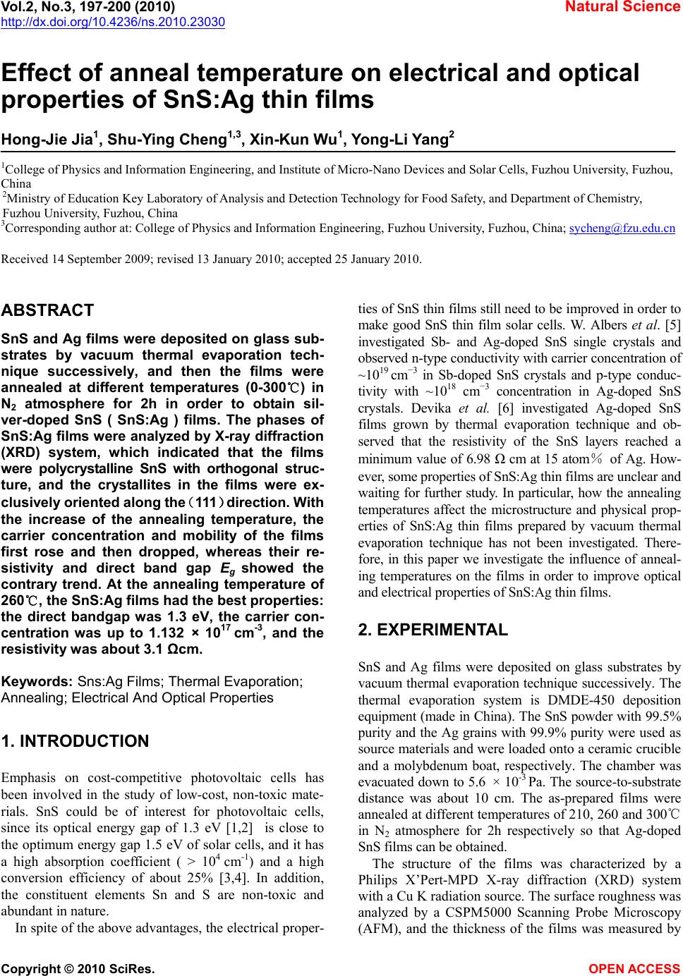
Effect of anneal temperature on electrical and optical
properties of SnS:Ag thin films
Hong-Jie Jia1, Shu-Ying Cheng1,3, Xin-Kun Wu1, Yong-Li Yang2
1College of Physics and Information Engineering, and Institute of Micro-Nano Devices and Solar Cells, Fuzhou University, Fuzhou,
China
2Ministry of Education Key Laboratory of Analysis and Detection Technology for Food Safety, and Department of Chemistry,
Fuzhou University, Fuzhou, China
3Corresponding author at: College of Physics and Information Engineering, Fuzhou University, Fuzhou, China; sycheng@fzu.edu.cn
Received 14 September 2009; revised 13 January 2010; accepted 25 January 2010.
ABSTRACT
SnS and Ag films were deposited on glass sub-
strates by vacuum thermal evaporation tech-
nique successively, and then the films were
annealed at different temperatures (0-300℃) in
N2 atmosphere for 2h in order to obtain sil-
ver-doped SnS ( SnS:Ag ) films. The phases of
SnS:Ag films were analyzed by X-ray diffraction
(XRD) system, which indicated that the films
were polycrystalline SnS with orthogonal struc-
ture, and the crystallites in the films were ex-
clusively oriented along the(111)direction. With
the increase of the annealing temperature, the
carrier concentration and mobility of the films
first rose and then dropped, whereas their re-
sistivity and direct band gap Eg showed the
contrary trend. At the annealing temperature of
260℃, the SnS:Ag films had the best properties:
the direct bandgap was 1.3 eV, the carrier con-
centration was up to 1.132 × 1017 cm-3, and the
resistivity was about 3.1 Ωcm.
Keywords: Sns:Ag Films; Thermal Evaporation;
Annealing; Electrical And Optical Properties
1. INTRODUCTION
Emphasis on cost-competitive photovoltaic cells has
been involved in the study of low-cost, non-toxic mate-
rials. SnS could be of interest for photovoltaic cells,
since its optical energy gap of 1.3 eV [1,2] is close to
the optimum energy gap 1.5 eV of solar cells, and it has
a high absorption coefficient ( > 104 cm-1) and a high
conversion efficiency of about 25% [3,4]. In addition,
the constituent elements Sn and S are non-toxic and
abundant in nature.
In spite of the above advantages, the electrical proper-
ties of SnS thin films still need to be improved in order to
make good SnS thin film solar cells. W. Albers et al. [5]
investigated Sb- and Ag-doped SnS single crystals and
observed n-type conductivity with carrier concentration of
~1019 cm−3 in Sb-doped SnS crystals and p-type conduc-
tivity with ~1018 cm−3 concentration in Ag-doped SnS
crystals. Devika et al. [6] investigated Ag-doped SnS
films grown by thermal evaporation technique and ob-
served that the resistivity of the SnS layers reached a
minimum value of 6.98 Ω cm at 15 atom% of Ag. How-
ever, some properties of SnS:Ag thin films are unclear and
waiting for further study. In particular, how the annealing
temperatures affect the microstructure and physical prop-
erties of SnS:Ag thin films prepared by vacuum thermal
evaporation technique has not been investigated. There-
fore, in this paper we investigate the influence of anneal-
ing temperatures on the films in order to improve optical
and electrical properties of SnS:Ag thin films.
2. EXPERIMENTAL
SnS and Ag films were deposited on glass substrates by
vacuum thermal evaporation technique successively. The
thermal evaporation system is DMDE-450 deposition
equipment (made in China). The SnS powder with 99.5%
purity and the Ag grains with 99.9% purity were used as
source materials and were loaded onto a ceramic crucible
and a molybdenum boat, respectively. The chamber was
evacuated down to 5.6 × 10⁻³ Pa. The source-to-substrate
distance was about 10 cm. The as-prepared films were
annealed at different temperatures of 210, 260 and 300 ℃
in N2 atmosphere for 2h respectively so that Ag-doped
SnS films can be obtained.
The structure of the films was characterized by a
Philips X’Pert-MPD X-ray diffraction (XRD) system
with a Cu K radiation source. The surface roughness was
analyzed by a CSPM5000 Scanning Probe Microscopy
(AFM), and the thickness of the films was measured by