Int'l J. of Communications, Network and System Sciences
Vol.2 No.6(2009), Article ID:702,8 pages DOI:10.4236/ijcns.2009.26064
A Low Power and High Speed Viterbi Decoder Based on Deep Pipelined, Clock Blocking and Hazards Filtering
1Department of Information Technology, Sri Venkateswara College of Engineering, Chennai, Tamilnadu, INDIA
2Department of Electronics and Communication Engineering, PSNA College of Engineering and Technology, Dindigul, Tamilnadu, INDIA
Email: carunme@yahoo.com, rajavmani@rediffmail.com
Received May 18, 2009; revised July 14, 2009; accepted August 23, 2009
Keywords: Viterbi Decoder, Convolutional Codes, High-Speed, Low Power Consumption, Parallel Processing, Deep Pipelining.
ABSTRACT
A high speed and low power Viterbi decoder architecture design based on deep pipelined, clock gating and toggle filtering has been presented in this paper. The Add-Compare-Select (ACS) and Trace Back (TB) units and its sub circuits of the decoder have been operated in deep pipelined manner to achieve high transmission rate. The Power dissipation analysis is also investigated and compared with the existing results. The techniques that have been employed in our low-power design are clock-gating and toggle filtering. The synthesized circuits are placed and routed in the standard cell design environment and implemented on a Xilinx XC2VP2fg256-6 FPGA device. Power estimation obtained through gate level simulations indicated that the proposed design reduces the power dissipation of an original Viterbi decoder design by 68.82% and a speed of 145 MHz is achieved.
1. Introduction
Overcoming the variable deterioration in reliability of a communication channel in real time is a critical issue for many communication systems. Therefore, from the channel coding point of view techniques, this demands both high speed and low power decoding. Convolution code and Viterbi algorithm are known to provide a strong forward error correction scheme, which have been widely utilized in noisy digital communication applications like satellite and wireless communication. For the decoder part, maximum likelihood method has been used in Viterbi decoding [1].The types of convolution codes qualified in the 3GPP WCDMA mobile communication system are (561,753) and (557, 663,711). It requires high decoding speed and low power consumption because of the large constraint value [2].
A conventional Viterbi decoder contains three major units: 1) a Branch Metric Unit (BMU) which calculates the branch metrics; 2) an Add-Compare-Select Unit (ACSU) which recursively accumulates the branch metrics as the path metrics (PM), compares the incoming path metrics, and makes a decision to select the most likely state transitions for each state of the trellis and generates the corresponding decision bits; and 3) a survivor memory unit (SMU), which stores the decision bits and helps to generate the decoded output. Among these three units, the ACSU and SMU consume most of the power of the decoder [3].
To meet the high throughput requirement of the modern communication systems, the fully parallel and pipelined architecture is commonly used for implementing the Viterbi decoder [4]. Many ACSs run at a high clock frequency and hence they consume a lot of power. Simultaneously, the SMU also consumes more power because of the large number of memory accesses. In some cases, it is more than half of the total power consumption of the decoder [5]. There are two known methods for the implementation of the SMU, namely the Register Exchange method (RE) and the Trace Back (TB) method [6]. In general, RE has the advantage of high speed, low latency, and simple control but it consumes more power than the Traceback (TB) mechanism since it needs to move the data among the memories in every cycle. Therefore, the TB mechanism is commonly used for the implementation of the SMU.
Numerous methods have been studied reduce the power consumption of the Viterbi decoder by exploiting different aspects of the system characteristics. The sliding block VD architecture was designed to achieve a speed of 1Gbps [7]. The decoding in the sliding block decoder was performed simultaneously in forward and backward direction. However, only a 4-state Viterbi decoder was implemented, while for practical 32- or 64-state Viterbi decoder, the complexity of the decoder is extremely high due to the fully parallel ACS units and large number of skew buffer registers required. Inside the Viterbi decoder, the feedback loop in the Add-Compare-Select (ACS) unit imposes the bottleneck on the decoding speed and shorten the critical path in the ACS unit has been widely studied [7]. A retiming scheme for the most significant bit (MSB) first ACS unit was analyzed in detail to achieve minimal length of the critical path [8]. A bidirectional Viterbi decoder that can meet the requirements of high-speed and low power consumption has been discussed by Song Li [2]. It can decode in both positive direction and reverse direction simultaneously, so that the decoding delay can be reduced to half of the unilateralism decoder. However, since the power consumption will greatly increase, it is obviously not worth implementing a bi-directional decoding through doubling the area and storage space.
The adaptive decoder discards some states (in the trellis) with high path metrics dynamically during the decoding process [9]. Seki et al. suggested the use of a scarce state transition (SST) scheme for the multimedia mobile communication [10]. The scheme employs a simple pre-decoder followed by a pre-encoder to minimize signal transitions at the input of a conventional Viterbi decoder, which leads to lower dynamic power dissipation. Kong and Willson studied various issues in designing a low-power Viterbi decoder for the IS-95 CDMA system. Their decoder employs various low-power design schemes such as state partition, gated control, and gray coding [11]. A k-pointer algorithm was studied for the efficient implementation of the TB-based SMU design [6]. In this implementation, several memory READ operations were required in order to decode one bit. Thus, the power consumption due to the memory access operation was significant.
Limited search algorithms were used to reduce the average number of ACS computation and the path storage required by Viterbi Algorithm (VA) [12]. The T-algorithm requires comparison operations for finding the best path metric in each decoding stage. This limits the use of the T-algorithm for high throughput applications. For low throughput applications, the comparisons can be done in multiple cycles. Many T-algorithms were designed for the low throughput applications [13,14]. The SPEC-T algorithm was implemented to solve the problem by relieving the requirement of finishing the comparison in one cycle to v cycles, where v is the latency of the comparison operation. The current best path metric was estimated with errors and then corrected for every v cycles. However, it still has large power and area overhead to search for the best path metric [15].
During the trace-back operation, the decision bits of all the states were read out from the memory at the same time, but actually only one bit is required. Thus, the power overhead was large. The power overhead of the trace-back operation was reduced by dividing the original memory, which had a word length equal to 2K-1, into two equal and smaller memories [16]. The power efficiency of the T -algorithm had been demonstrated in by assuming 2K-1 banks of 1-bit memories were used [5]. However, the hardware implementation was not described. Also, the area for this memory configuration was large and the power overhead of the peripheral can be high which makes the cost of adoption of this memory configuration very high.
In order to improve the speed and reduce the power consumption we proposed new architecture incorporate the ACS and TB and their associated circuits for decoding process have been operated in parallel and deep pipelined manner for higher date rate. For a low-power design we proposed a clock gating and toggle filtering for survivor path and trace back units of Viterbi decoder. The design of a decoder at behavior level has been described in a high-level hardware description language. The behavioral design is synthesized to generate a gate level design. For testing the behavioral design MODEL SIM has been used. We compared the gates utilization, speed and power dissipation of the different implementation and suggested a low power and high speed Viterbi decoder design The paper is organized as follows Section 2 presents the algorithm and operation of Viterbi decoder. The architecture of the proposed Viterbi decoder is described in Section 3. Section 4 describes the operation of deep pipelined mechanisms. Section 5 comprises of the proposed low power techniques. FPGA implementation and performance are given in Section 6.
2. Viterbi Decoder Algorithm
In this section, both the algorithm and operation behind the proposed eight state Viterbi decoder depicted in Figure 1 are presented. Consider a communication system where the convolutional encoder adds redundancy to the input signal S, and the encoded output x symbols are transmitted over a noisy channel.
The input of the convolutional decoder that is the input for the Viterbi decoder r is the encoded symbols contaminated by noise. Then the decoder tries to extract the original information from the received sequence and generates an estimate y. The algorithm that maximizes
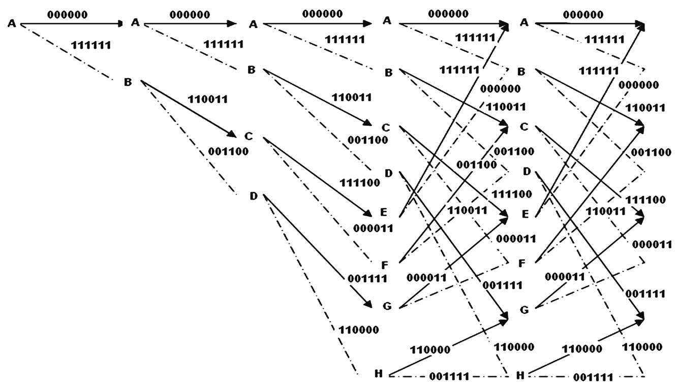
Figure 1. A 8–state Trellis diagram for K=4.
the conditional probability P (r|y) is called the maximum likelihood algorithm.
The maximum-likelihood algorithm finds the most likely code sequence for the received channel output sequence. Therefore, if the encoder output sequence is denoted by xm, and the channel output sequence is denoted by r, the probability of receiving r when the channel input is xm is
 (1)
(1)
The most likely path through the trellis for the channel output r is the one that maximizes the function. Thus, the function shown in Equation (1) is usually called the metric and it is used in comparison between the code sequence and the received sequence [6]. Notice that the decoding metric in Equation (1) requires product implementation and therefore the metric ln [Pr (r|xm)] is more frequently applied than the metric Pr (r|xm) in the decoder. Moreover, finding the trellis path with the largest log-likelihood function corresponds to the maximum likelihood decoding.
 (2)
(2)
where the components of the summation are accumulated on the individual branches, and therefore they are denoted by branch metrics. In this work, the hard-decision decoding method is used, and is determined using the Hamming distance measure. Thus, the most optimal path through the trellis is the path with the minimum Hamming distance. The Hamming distance between the trellis code word  and the received sequence
  each of them being of length n is:
 (3)
(3)
3. Proposed VLSI Architecture
There are two types of architectures for the implementation of Viterbi decoder: register exchange method and memory trace back method. The register-exchange algorithm offers minimal latency as required. Unfortunately, the capacitive load of clock and trellis-structured interconnect network dissipate considerable power, and their routing resources occupy significant area [12]. Register traceback method was proposed in order to reduce the interconnect wires and power from register exchange method. But this architecture still consumes lots of logic materials, and the critical paths are too long to improve the speed [1]. In this paper we have presented two schemes to reduce power dissipation in the traceback approach. The proposed architecture of Viterbi decoder is presented in Figure 2 for reducing power.
3.1. Branch Metric (BM) Module
The BM module generates branch metric for ACS module in terms of the received channel symbols; the architecture of BM is very straightforward. The only point to be mentioned here is that, in order for the constrain length to be reconfigured, a set of RAMs are employed to provide branch information for branch metric computation, in terms of the constraint length selection. Obviously, a pipeline scheme can be easily applied to achieve enough high speed for branch metric calculations, because of no feedback loop existing in the BM module.
3.2. ACS Module
For each state in the trellis diagram of Viterbi decoding, current path metrics are obtained from current branch metric and path metrics of the previous states, which lead to current state, by executing addition, comparison and selection operations. We modified the regular ACS structure to deep pipelined structure in order to speed up this module.
3.3. Traceback Module
The TB module is a bank of registers, which record the survivor path of each state selected by the ACS module. A register is assigned to each state, and the length of a register is equal to the frame length (which is 24 for our decoder). The corrected output sequence is produced by tracing the decision vectors. The traceback module is used to decide the final output.
4. Proposed Pipelined and Deep Pipelined Structure
The speed of the decoder can be improved by applying pipelining approach to ACS and TBU shown in Figure 3. Pipelining is performed between BMU, ACS and TBU where multiple instructions are overlapped in execution. Pipelining does not decrease the time for individual instruction execution. Instead, it increases instruction throughput and is determined by how often it exits the pipeline.
To obtain high speed implementation, the maximum inherent parallelism needs to be extracted. Generally, a high throughput rate is achieved if the circuit has a very short critical path. The critical path of a synchronous circuit is that path between two buffers that has the largest delay and hence determines the maximum achievable clock frequency of the circuit. The pipeline register block consists of a set of positive edge triggered D-type flip
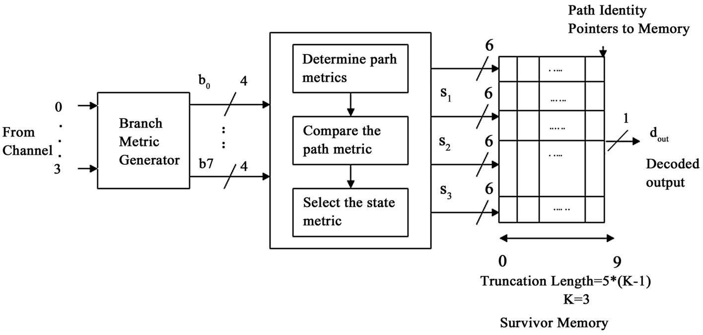
Figure 2. Architecture of Viterbi decoder.
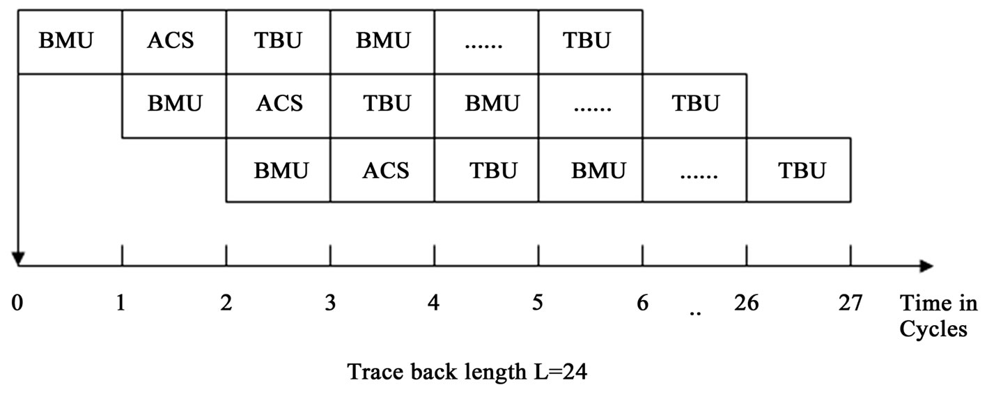
Figure 3. Parallel and pipelined execution of Viterbi decoder.
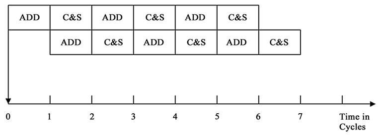
Figure 4(a). Deep pipelined execution of ACS (Add-Compare-Select) unit.
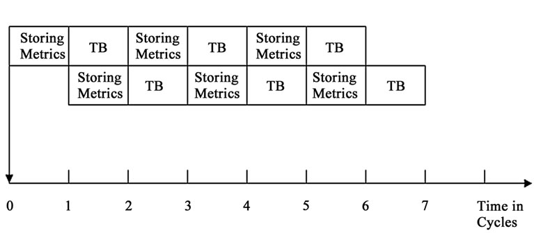
Figure 4(b). Deep pipelined execution of Trace Back (TB) unit.
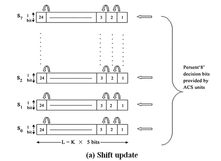
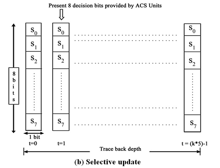
Figure 5. Shift update versus selective update.
flops. The total number of flip flops required is equal to the number of states multiplied by the number of state metrics bits, i.e. 8*6=48.
The throughput is still increased when deep pipelining method is used. In this method, the pipelining process is applied within ACS and TB units up to the trace back depth. Compared to others methods, deep pipelining method shows a tremendous reduction in memory usage and the throughput of the chip also increases considerably. In non-pipelined system the silicon area required is high and that results in high power consumption. This is considerably reduced in deep pipelining method whose structure is shown in Figure 4.
5. Proposed Low Power Design
The two basic approaches used to record survivor paths are register-exchange and traceback. Both methods cause substantial switching activity and hence are inefficient in power dissipation. In this section, we have presented two schemes to reduce power dissipation in the traceback approach.
5.1. Survivor Path Storage Block and Clock Gating
In the traceback approach, one flip-flop is necessary to record the survivor branch for each state per stage. The shift update scheme forms a shift register for each state by collecting the flip-flops in the horizontal direction as shown in Figure 5(a). The survivor branch information is filled into the least significant bits of the registers. We have proposed the formation of registers vertically as shown in Figure 5(b). The survivor branch information is filled into registers from left to right as time progresses. This scheme is called selective update.
The key difference between the two schemes is that the content of a register in the selective update method does not change once it is updated. Hence, the register incurs less switching activity, thus reducing power dissipation. Moreover, the fact makes it possible to apply a clock-gating scheme to further reduce power dissipation. The clock of each register is enabled only when the register updates its survivor path information. Figure 6 shows the proposed survivor path storage block for the selective update method with employment of clockgating. In the figure, register Ri holds the survivor path information of all the states at stage i, where i is 1 to 24 for our decoders. The five-bit counter keeps track of the current stage, which is equal to the number of code symbols received so far for the frame. When the ith code symbol is received, the clock of register Ri is enabled, and the survivor path information of all the states at stage i is recorded in the register. Note that all the other registers hold their state since the clock of the other registers
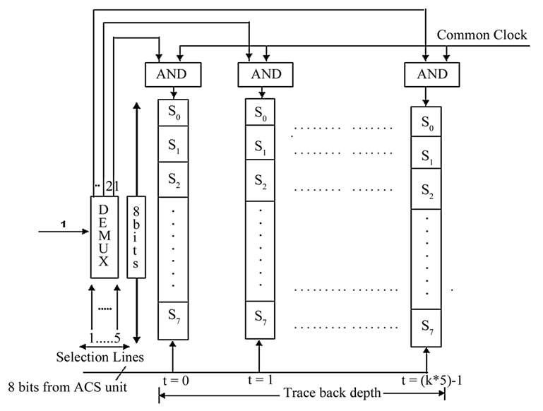
Figure 6. Proposed survivor path storage block for the selective update with clock gating.
is disabled. Therefore the proposed survivor path storage reduces switching activity to a minimal level to save power. Finally, it is possible to replace the five-bit counter and the de-multiplexer with a ring-counter.
5.2. Toggle Filtering of the Output Generator Block
The output generator block in the traceback approach traces back the survivor path after all the symbols have been received and generates the decoded output sequence. The block is a combinational circuit, which can be active only during one clock cycle.
A block diagram of the output generator block is shown in Figure 7. Ignoring the AND gates with an enable input for the time being, the block receives inputs from the survivor storage block containing the survivor path information. The block traces the survivor path at the end of the frame and generates the decoded output sequence. The decoded output sequence is loaded into a register at the first clock.
Since the registers update the survivor path information progressively throughout the entire frame, the output generator receives spurious inputs, which cause unnecessary switching activity to dissipate power. The proposed design blocks spurious inputs applied to the block. The array of AND gates and the enable signal shown in Figure 7 are introduced for this purpose. The enable signal is activated during the one clock period at the end of the frame as shown in Figure 7.
6. Implementation and Performance Results
We measured the speed, power and area of the three different implementations of Viterbi decoders: proposed deep pipelined design, the traceback approach with the clock gating and toggle filtering scheme.
We implemented the three different Viterbi decoders in the standard cell environment. It is first, we described the three Viterbi decoders at the register transfer level in VHDL. Then synthesized and placed and roughed using Xilinx project Navigator tool. The processing technology used in our experiments was CMOS six metal layer 0.25 μm with the supply voltage of 1.8V.
Power dissipation was estimated for the synthesized gate-level circuits using Xilinx project Navigator tools. The process for power estimation is calculated by using the maximum numbers of random patterns were simulated at the clock frequency of 10 MHz for each Viterbi decoder, and the switching activity of each node was recorded. Then, the power dissipation of the circuit was estimated using the formula, P=αCV2f, where α is the switching activity, C is the parasitic capacitance (0.032pF), V is the supply voltage (1.8V), and f is the clock frequency. The clock frequency was set to 10 MHz [6]. The static power dissipation of cells was not considered due to the limitation of the library cells used in our experiments.
Experimental results for three Viterbi decoders are shown in Table 1. Among the three designs, the conventional trace back approach has the largest area and the proposed low-power design the least area. The area of the proposed deep pipelined with low power design is 69% less than that of the conventional traceback approach and 36.5% less than that of shift and selective update low power approach. We observed that the large area for the conventional traceback is due to the complexity of the survivor path storage block. Table 1 Gates count, power dissipation and speed comparison of proposed three Viterbi decoders (Xilinx Vertex 2p)
The power dissipation of the three decoders is small due to the small size of the decoders and is in the range of 0.5 mW to 2 mW. The conventional traceback approach dissipates the largest amount of power, while the
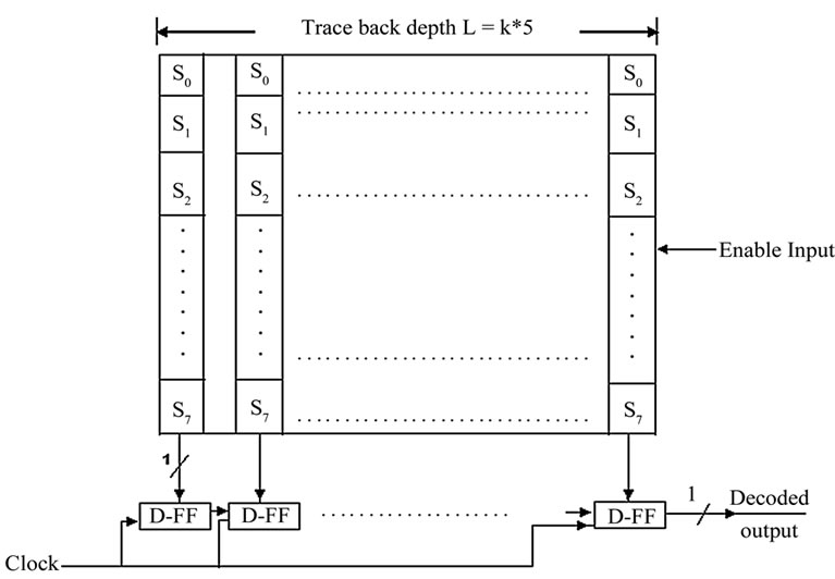
Figure 7. Proposed toggle filtering of the trace back block diagram.
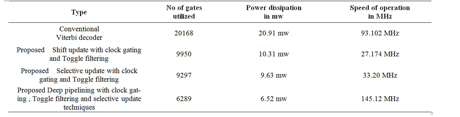
Table 1. Area, power dissipation and speed comparison of proposed methods.
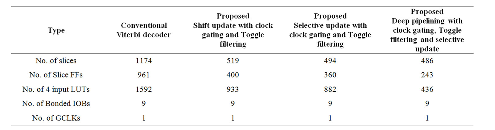
Table 2. Device utilization summary of three different decoders.
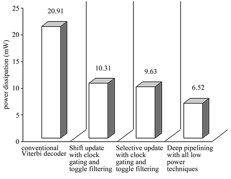
Figure 8. Power dissipation chart of four different implementation of Viterbi decoder.
proposed low-power design dissipates the least power. The proposed method reduces the power dissipation by 68.82% compared with the conventional traceback approach by 36.7% compared with the shift and selective update approach. We observed that the deep pipelined selective update scheme with clock gating and toggle filtering is the most effective method in power saving. Details on the experiments, including the area of each block and the power dissipation for three different decoders, are shown in Table 1&2. Figure 8 shows the power dissipation for the four different implementation of Viterbi decoder. The first bar in the Figure 8 is the power dissipation of original Viterbi decoder without low power techniques. When both the clock gating and toggle filtering is applied to s selective update deep pipelined Viterbi decoder in traceback approach, it saves about 68.82% of power compared with conventional Viterbi decoder.
7. Conclusions
Viterbi decoders employed in digital wireless communications are complex and dissipate high power. In this paper, we have investigate power dissipations of three different implementations of Viterbi decoders: the shift update, selective with clock gating and toggle filtering and deep pipelined with all low power techniques Viterbi decoder Scheme. We have proposed a low-power Viterbi decoder design based on the traceback approach. The schemes employed for our low-power design are clockgating of the survivor path storage block and toggle filtering of output generation block. We have implemented the three designs in the standard cell design environment and measured the performance in terms of area and power dissipation. Among the three implementations, it is observed that the proposed low-power design takes the smallest area and dissipates the least power. The proposed design reduces the power dissipation of the register-exchange approach by 68.82%. Finally, it is difficult to make a head-to-head comparison of power efficiency between the proposed method and other existing methods due to different environments (such as hard decision versus soft decision) and constraints imposed. Some of our techniques can also be applied to other low-power designs to save power.
8. References
[1] H. Yang and X. Lang, “Design and implementation of high speed and area efficient Viterbi decoder,” IEEE, Proceedings of the 8th International Conference on Solid State and Integrating Circuit Technology, ICSICT’06, pp. 2108–2110, 2006.
[2] S. Li and Q. M. Yi, “The design of high speed and low power consumption bidirectional Viterbi decoder,” IEEE, Proceedings of the 5th International Conference on Machine Learning and Cybernetics, Dalian, pp. 13–16, August 2006.
[3] J. Jin and C. Y. Tsui, “Low-power limited-search parallel state Viterbi decoder implementation based on scarce state transition,” IEEE Transaction on Very Large Scale Integration (VLSI) System, Vol. 15, No. 10, October 2007.
[4] C. C. Lin, Y. H. Shih, H. C. Chang, and C. Y. Lee, “Design of a power-reduction Viterbi decoder for WLAN applications,” IEEE Transactions on Circuits System I, Regular Papers, Vol. 52, No. 6, pp. 1148–1156, June 2005.
[5] R. Henning and C. Chakrabarti, “An approach for adaptively approximating the Viterbi algorithm to reduce power consumption while decoding convolutional codes,” IEEE Transactions on Signal Processing, Vol. 52, No. 5, pp. 1443–1451, May 2004.
[6] G. Feygin and P. Gulak, “Architectural tradeoffs for survivor sequence memory management in Viterbi decoders,” IEEE Transactions on Communications, Vol. 41, No. 3, pp. 425–429, March 1993.
[7] P. J. Black and T. H. Y. Meng, “A 1-Gb/s, four-state, sliding block Viterbi decoder,” IEEE Journal of SolidState Circuits, Vol. 32, No. 6, pp. 797–805, June 1997.
[8] K. K. Parhi, “An improved pipelined MSB-first add compare select unit structure for Viterbi decoders,” IEEE Transactions on Circuits and Systems I: Fundamental Theory and Applications, Vol. 51, No. 3, pp. 504–511, March 2004.
[9] M. H. Chan, W. T. Lee, M. C. Lin, and L. G. Chen, “IC design of an adaptive Viterbi decoder,” IEEE Transactions on Consumer Electronics, Vol. 42, pp. 52–61, February 1996.
[10] K. Seki, S. Kubota, M. Mizoguchi, and S. Kato, “Very low power consumption Viterbi decoder LSIC employing the SST (Scarce State Transition) scheme for multimedia mobile communications,” Electronics-Letters, IEE, Vol. 30, No. 8, pp. 637–639, April 1994.
[11] Kang and A. N. Willson, “Low-power Viterbi decoder for CDMA mobile terminals,” Conference-Paper, JournalArticle, IEEE Journal of Solid-State Circuits, Vol. 33, No. 3, pp. 473–82, March 1998.
[12] R. Henning and C. Chakrabarti, “An approach for adaptively approximating the Viterbi algorithm to reduce power consumption while decoding convolutional codes,” IEEE Transactions on Signal Processing, Vol. 52, No. 5, pp. 1443–1451, May 2004.
[13] R. Tessier, S. Swaminathan, R. Ramaswamy, D. Goeckel, and W. Burleson, “A reconfigurable, power-efficient adaptive Viterbi decoder,” IEEE Transactions on Very Large Scale Integration (VLSI) System, Vol. 13, No. 4, pp. 484–488, April 2005.
[14] M. Guo, M. O. Ahmad, M. N. S. Swamy, and C. Wang, “FPGA design and implementation of a low-power systolic array-based adaptive Viterbi decoder,” IEEE Transactions on Circuits Systems I, Regular Papers, Vol. 52, No. 2, pp. 350–365, February 2005.
[15] F. Sun and T. Zhang, “Parallel high-throughput limited search trellis decoder VLSI design,” IEEE Transactions on Very Large Scale Integration (VLSI) System, Vol. 13, No. 9, pp. 1013–1022, September 2005.
[16] Y. N. Chang, H. Suzuki, and K. K. Parhi, “A 2-Mb/s 256-state 10-mW rate-1/3 Viterbi decoder,” IEEE Journal on Solid-State Circuits, Vol. 35, No. 6, pp. 826–834, June 2000.