Journal of Modern Physics
Vol.2 No.9(2011), Article ID:7145,7 pages DOI:10.4236/jmp.2011.29124
Density of States in Intrinsic and n/p-Doped Hydrogenated Amorphous and Microcrystalline Silicon
1Laboratoire de Physique Théorique et Physique des Matériaux, Université de Hassiba Ben Bouali, Chlef, Algeria
2Laboratoire de Physique des Couches Minces et Matériaux pour l’Electronique, Institut de physique,
Université d’Oran Es-Senia, Oran, Algeria
3Centre de Fisica Molecular Complexo I, IST, Lisbona, Portugal
E-mail: f.larbi@yahoo.fr
Received June 13, 2011; revised July 22, 2011; accepted July 30, 2011
Keywords: Defects Formation, Doping, Microcrystalline Silicon, Thermodynamic Model of Defect, Optical Properties and Measurements
ABSTRACT
Gap states in amorphous hydrogenated silicon (a-Si:H) doped and microcrystalline silicon doped n and p were examined by analysis of subgap absorption spectra obtained by the Constant Photocurrent Method (CPM) and the Photothermal Deflection Spectroscopy (PDS). Assuming a Gaussian distribution of defect states in the gap, broad distribution of states was found in a-Si:H and doped a-Si:H. A dependence of the defect concentration on Fermi energy was detected and analysed by thermodynamic model of defect formation in a-Si:H.
1. Introduction
Over the last decade, attention has been paid to study hydrogenated microcrystalline silicon  because of its good optoelectronic properties, and stability against light-induced changes [1]. But the nature of density of gap states (DOS) of
  is still not well understood, because of structural heterogeneity of this material. Recently, Sanjay Ram et al. [2,3] proposed numerical simulation modelling using Shockley-Read statistics in steady state conditions which describe the effective DOS picture in
 .
.
The defect states in hydrogenated amorphous silicon (a-Si:H) and microcrystalline silicon act as trapping and/ or recombination centers, and affect the electronic devices performances based on these materials, such as solar cells. Photoconductivity measurements and PDS provide a simple way of obtaining information on the density of states in amorphous and microcrystalline semiconductors. The density of gap states can be considered as composed of tail states corresponding to Si-Si weak bond states and Si-dangling bond defect states. It is well known that the density of Si dangling bond states can be determined by chemical equilibrium process due to interconversion of weak and dangling bonds [4-6].
In this paper, we report experimental results of CPM obtained on defect states in a series of undoped and doped a-Si:H films and experimental measurement of PDS in  doped and intrinsic samples. The density of states in the gap of a-Si:H samples was examined by the deconvolution analysis of the subgap spectra. The dependence of the defect concentration on Fermi level was established and analyzed by thermodynamics model [7,8] based on the chemical equilibrium reaction between the weak and the dangling bonds involving the emission and trapping of hydrogen.
2. Experimental Details
 films were produced by reactive Radio Frequency Magnetron Sputtering deposition (RFMS). The sputtering chamber was evacuated to about 10–7 Torr. For the plasma gas mixture of 30% Argon and 70% H2, the power density of 0.9 W·cm–2 used to excite the plasma and target-sample holder distance of 70 mm was maintained constant for all the samples. For each of the two doping (n) and (p) and intrinsic samples, we used a 100˚C substrate temperature and a 30 minute deposit time. The total pressure was maintained constant at 3 Pa and the films thickness (d) was typically about
  for all samples.
a-Si:H samples were prepared by conventional Plasma Enhanced Chemical Vapour Deposition (PECVD) using a standard reactor configuration [9]. Doping of plasma was achieved by adding phosphine (PH3) or diborane (B2H6) gases to plasma. The samples were deposited at different substrate temperatures. Prior to the deposition phase, the pressure and RF power were varied and the partial pressure of doping gas was taken at selected values from 0.5% to 1.5%. The parameters of deposition are summarized in Table 1. The films were deposited on glass substrate Corning (7059). Evaporated coplanar aluminium electrodes were used for the measurement of the conductivity and photoconductivity. The Tauc optical gap (ETauc), the thickness (d) and the absorption coefficient α for the most absorbed wavelength were determined from the measurement of optical transmission in the wavelength ranging from 400 nm to 2400 nm. The constant photocurrent method (CPM) was used to measure the subgap absorption.
3. Results and Discussions
3.1. Defects Density Models in a-Si:H
For a-Si:H, various methods have been proposed for evaluated the deep defect density (ND) in a-Si:H density of states (ND) via optical absorption spectra, we quote in particular studies:
![]() Jackson and Amer [10] proposed for evaluated the deep defect density ND in a-Si:H a method based on the integration the excess absorption in the weak energies, estimated by subtracting from the measured absorption
Jackson and Amer [10] proposed for evaluated the deep defect density ND in a-Si:H a method based on the integration the excess absorption in the weak energies, estimated by subtracting from the measured absorption  the contribution of the transitions involving states located in the bandtails, obtained by extrapolation of the exponential part of the edge of absorption according to:
 (1)
(1)
where  is Urbach energy, can be considered equal to the valence bandtail
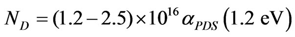
 . The apparent Urbach energy Eov, which characterize the disorder and consequently the weak Si-Si bonds is usually determined by the linear regression in the exponential range (Figure 1). The term of proportionality (7.9 × 10¹⁵) was determined by the good correlation enter the defect density deducted in certain samples of a-Si:H and the defect density paramagnetic determined by the EPR technique, defects were identified by their factor g = 2.0055 as neutral hanging connections D˚.
It is necessary to note that this method is widely used in the case of a-Si:H, and criticized for several reasons:
![]() i-It takes into account the neutral hanging connections only, while it can have defects without spin contributing to the optical absorption.
i-It takes into account the neutral hanging connections only, while it can have defects without spin contributing to the optical absorption.
![]() For the worst samples the defect density is very important, we can have a covering in energy enter the optical absorption involving the deep states and those bringing in states localized in the bantails, what leads then to one under estimation of the excess absorption and the defect density ND.
For the worst samples the defect density is very important, we can have a covering in energy enter the optical absorption involving the deep states and those bringing in states localized in the bantails, what leads then to one under estimation of the excess absorption and the defect density ND.
![]() The optical absorption in a reference energy was
The optical absorption in a reference energy was
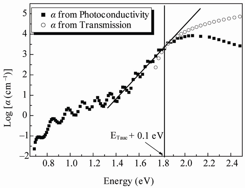
Figure 1. The CPM spectra were normalized to the transmission measurement. The extrapolation of the Urbach tail equal to Tauc plot at .
.

Table 1. Substrate temperature (Ts), thickness (d), RF power, partial pressure of doping (P.P).
widely used in the case of a-Si:H and even for has it a-Ge:H. This value of absorption can be directly correlated in the defect density, and the choice of the reference energy (in little meadows in the middle of the gap [11] or in the intersection of the exponential edge with the axis of the energies [12]) has no other purpose than to define a scale of comparison between the various samples. Among the authors who used this method, we quote in the case of a-Si:H, Yamasaki et al. [13] who showed a good correlation between the density of spins measured by EPR and the coefficient of absorption measured by the PDS at an energy of 1.2 eV according to the relation:
 (2)
(2)
![]() The fitting or deconvolution of the absorption spectra was also widely used and allowed to get very useful information on the DOS (Density of State) and at their distribution in the gap [14,15]. The principle of this method consists of using a model of DOS suitable to the tetracoordinated amorphous semiconductors [16], to calculate numerically the coefficient of absorption, while modifying systematically the parameters of adjustments of the model to obtain a better reproduction of the experimental spectra on all the range of energy. For more information on this method one can be consult the reference [17].
The fitting or deconvolution of the absorption spectra was also widely used and allowed to get very useful information on the DOS (Density of State) and at their distribution in the gap [14,15]. The principle of this method consists of using a model of DOS suitable to the tetracoordinated amorphous semiconductors [16], to calculate numerically the coefficient of absorption, while modifying systematically the parameters of adjustments of the model to obtain a better reproduction of the experimental spectra on all the range of energy. For more information on this method one can be consult the reference [17].
For the analysis of the absorption spectra, withdrawn from CPM measurement, we used the method of deconvolution and we have developed the necessary programs for the numeral calculation to get information on the defects density of states in the gap and at their distribution in energy.
3.2. Deconvolution Model and Deep Defect Density
We fit theoretical model for a-Si:H gap state density to the measured optical absorption spectra in order to estimate a more accurate value of the Urbach energy and the deep defect density ND. The principal characteristics of this deconvolution procedure are:
![]() The conduction band mobility edge taken as the origin of energies;
The conduction band mobility edge taken as the origin of energies;
![]() The conduction and the valence bands are supposed parabolic;
The conduction and the valence bands are supposed parabolic;
![]() The conduction and the valence band tails are described by exponential distribution.
The conduction and the valence band tails are described by exponential distribution.
![]() The deep-gap states are represented by a Gaussian distribution centred at ED below the conduction and mobility edge Ec.
The deep-gap states are represented by a Gaussian distribution centred at ED below the conduction and mobility edge Ec.
After these assumptions we deconvolute the experimental absorption spectra by using the formula [18]:
 (3)
(3)
The integration is performed over all initial (filled) states with density 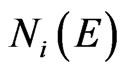 and all final (empty) states with density
 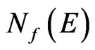 separated in energy by
 . The symbol
  is a factor depending on the refractive index and on the momentum matrix element, it can be assumed constant and equal to 1.8 × 10–38 cm3·eV2 for all the optical transitions involved provided the energy dependence on these parameters is neglected [19]. All the optical absorption spectra were analyzed by this procedure and fit well to the experimental data in Figure 2. The determination of Fermi level is obtained from the dark conductivity measurements by:
 (4)
(4)
where  is the pre-exponential factor, corresponding to the conductivity at infinite temperature,
  is the constant of Boltzmann and T represented the temperature.
The CPM spectra obtained were normalized to absolute values by fitting to the transmission measurements by setting the extrapolation of the Urbach tail equal to Tauc plot at energy E = ETauc + 0.1 eV [20]. The Tauc gap (ETauc) separating the extrema of the valence and conduction bands supposed parabolic and not perturbed by the disorder, by the extrapolation of the part strong absorption ( 103 cm–1 ) towards the weak energies according to the relation:
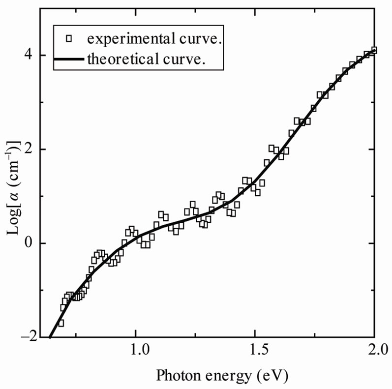
Figure 2. The open circle is the experimental absorption coefficient data and the solid line is the optical absorption spectra fit obtained by deconvolution procedure.
 (5)
(5)
Although the values of Tauc gap determined by this method are subject to pledge for the more or less thick layers, they follow the same variations as the energy E04 (correspond to ); the difference between the values of ETauc and of energy E04 remains appreciably constant.
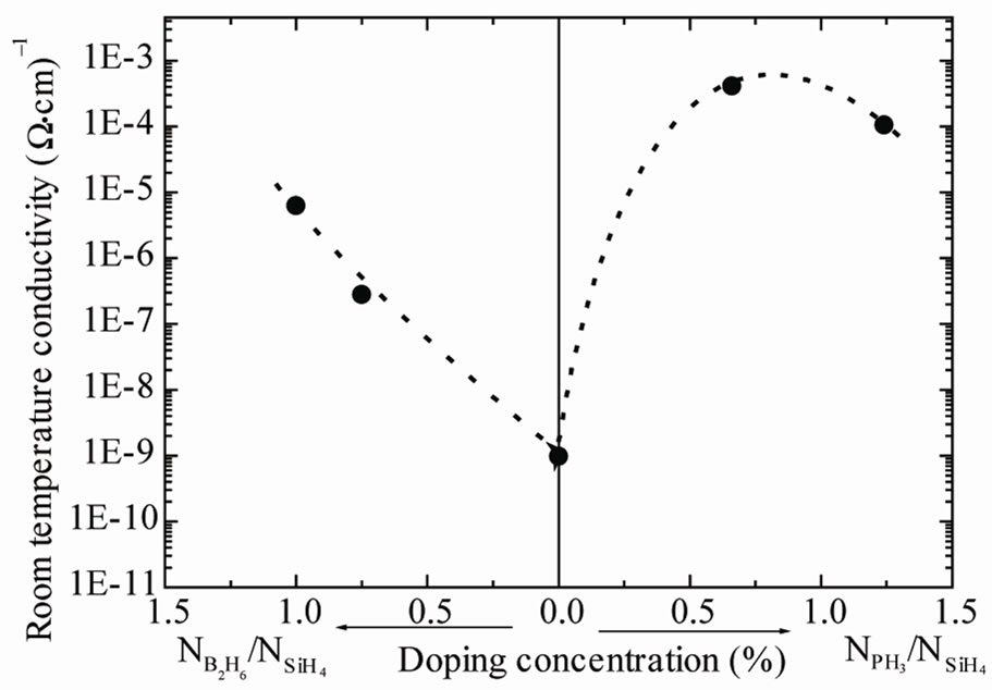
In the Figures 3(a) and (b) we represented the variations of the room temperature conductivity and dark conductivity activation energy versus the doping concentration of n and p-type a-Si:H. It clearly appears that the addition of small quantities of phosphine or diboranne to the deposition gas promotes a very high change factor (106) in the room temperature conductivity. The activation energy decreases from 0.8 eV in undoped material to about 0.2 eV with phosphorus doping and to 0.4 eV for boron. Previous experiments showed that the conductivity change was due to a shift of the Fermi energy, and
 (a)
(a)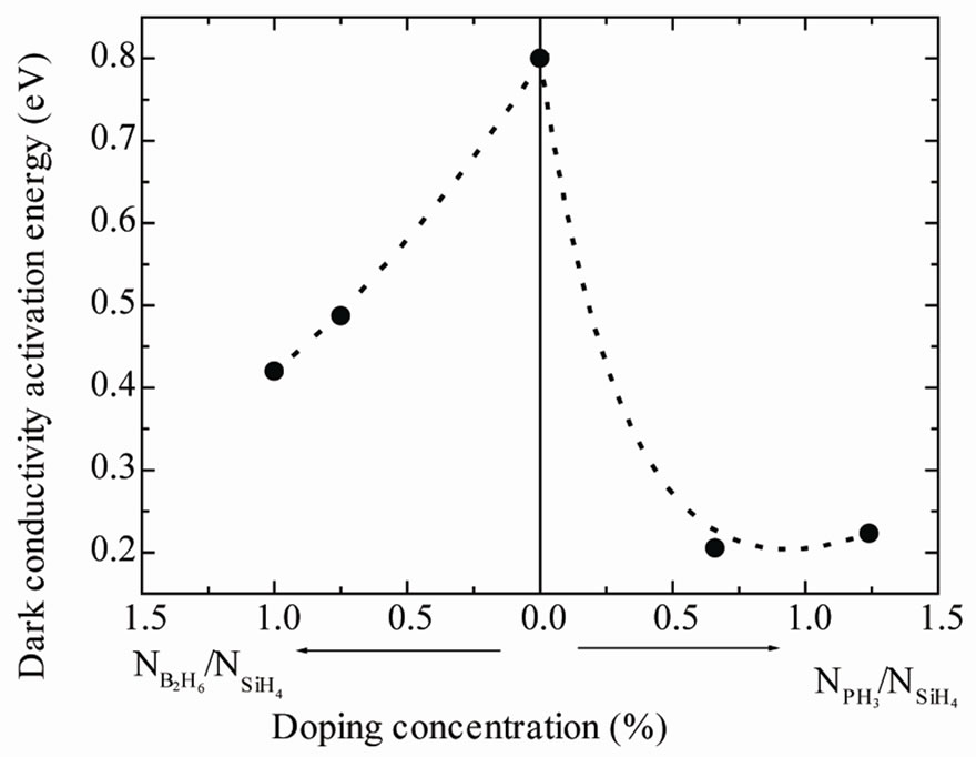 (b)
(b)
Figure 3. (a) The variation of the room temperature conductivity with the doping concentration of the phosphine and the diborane; (b) The dark conductivity activation energy versus the doping concentration of PH3 and B2H6.
that n-type and p-type conduction was occurring. These results show that the Fermi energy (EF) still remains in localized states and EF does not reach the conducting states above the mobility edge. This is due to the high density of bandtails localized states and also to the low doping efficiency. The conductivity is lower in p-type than in n-type samples. This can be attributed also at to the wider valence bandtail which keep EF farther from the mobility edge, and may be to the doping efficiency of boron which is lower than the phosphor doping efficiency.
Figure 4 compares the optical absorption spectra of phosphorus, boron doped and undoped a-Si:H. The addition of small quantities of phosphine or diborane to the deposition gas promotes caused an important increase in the level of absorption towards the weak energies. This increase of the level of absorption or deeper states is around two orders of magnitude for the doped spectra, although it is more important for the doped n with regard to the doped p. The inferred defect density increases with doping and is exactly the same in both n-type and p-type material at the same doping level. This observation is in concordance with the results obtained by the street analysis [21]. In this model it is assumed that in both case the n-type doping with phosphorus and p-type doping with boron are accompanied by the creation of the charged defect given by the following reactions:
Si04 + P30  P4+ + D–
Si04 + B30 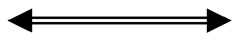 B–4 + D+
Some characteristic parameters of state density in the gap can be deduced by the analysis of the optical absorption spectra described in the first section. The fit of the absorption coefficient allows determining the Urbach energy E0V, the deep defect density ND and its energetic
Figure 4. The optical absorption spectra of phosphorus doped (open circle), boron doped a-Si:H (solid circle) and undoped a-Si:H (solid up triangle).
position with regard to the conduction band (EC – ED). Typical characteristic parameters are summarized in Table 2.
Important remarks can immediately be pointed out from the data listed in this table:
· The energy position of the neutral defect is situated at the middle of the gap EC – ED = 0.9 eV. However the energy of the positive and the negative charged dangling bonds are located at 0.6 eV and 1.2 eV from the conduction band edge respectively. This allows concluding that correlation energy can be estimated equal to 0.3 eV. deduced from relation: , were
  is the energy of positive or negative charged dangling,
  present the energy of neutral dangling and U corresponding the correlation energy.
· For the n-type, the displacement of the Fermi energy from the middle gap to conduction band edge promotes the displacement of the Gaussian center (ED) to the valence band edge. In the case of the ptype, when EF tends to the valence band edge, ED reaches the conduction band edge. We also remark that there is an important increase of the deep center density when the Fermi energy moves from the intrinsic level in the gap. These results can be explained by the model developed in the theory of defect formation in a-Si:H [7]. This last one is based on the thermodynamic analysis of few simple chemical reactions, where the neutral defect formation in undoped a-Si:H are described by the following reaction:
SiH + SiSi  D0 + SiHSi where SiH are the hydrogen atoms bonded to Si and SiHSi are the trapped hydrogen at a weak-bond site. To interpret the correlation between the Fermi level and the density of localized states, Winer [7], consider the additional reactions given by:
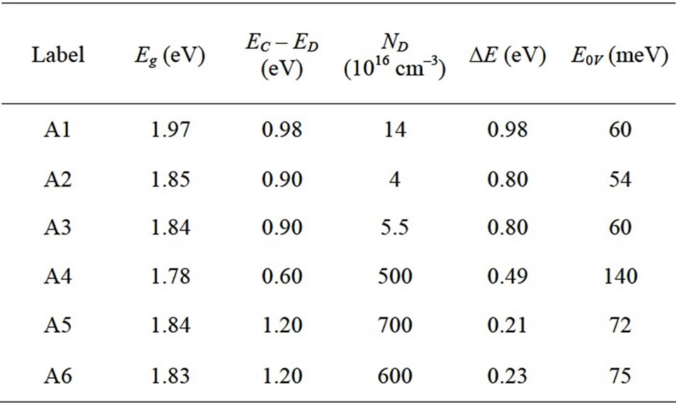
Table 2. Urbach energy E0V, deep defect density ND, defect energetic position EC – ED, gap mobility Eg, dark conductivity activation energy ∆E.
D0 + e– D–
D–
D0 + h+  D+
D+
In the forward direction, these describe the capture of electron from the conduction band and hole from the valence band by a neutral defect respectively. An increasing of the electron or hole number in the system pushes these reactions and consequently a creation of larger deep defect concentration. This process is independent of the extra electron and hole origin. Defect creation by this process can result from applied field, light exposure, doping, and all parameters can modify the position of the electronic neutrality level. Shift in the Fermi energy to fill or empty defect states leads to a change in their distribution. Further more the dependence of states density can be described in terms of defect formation theory developed by Winer [7] where the defect density is expressed by:
 (6)
(6)
where ED is the energy of the most probable defect configuration, k is the Boltzmann constant, T the temperature and µD the defect chemical potential. The defect chemical potential plays an important role in determining the equilibrium defect concentrations. We represented in Figure 5 the variation the defect concentration as function of Fermi energy for all samples. The calculated equilibrium charged defect concentrations exponentially increase with increasing separation of the Fermi energy
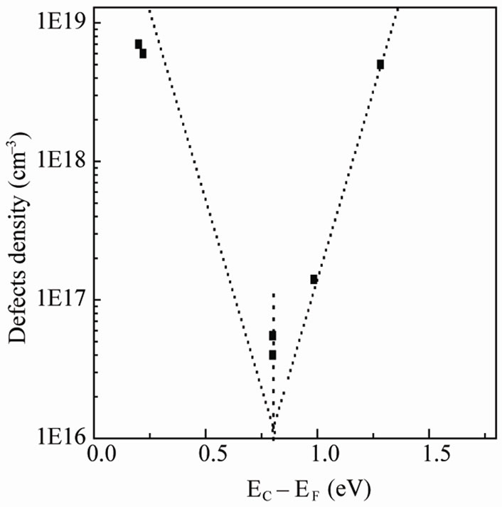
Figure 5. The defect concentration as function of Fermi level obtained by the absorption spectra deconvolution (solid square). The calculated equilibrium charged defect concentrations as function of the chemical potential dotted line with E0V ≈ 60 meV, EI = 0.9 eV, NV = 6.71021 cm–3·eV–1, EF and Eg are given by the Table 2.
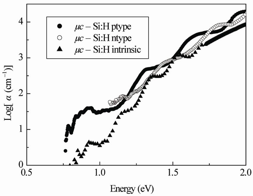
Figure 6. The optical absorption spectra of boron, phosphorous doped and intrinsic microcrystalline silicon 
 .
.
from midgap with a slope 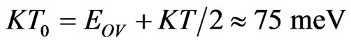 for n and p type a-Si:H. Although we have assumed that the intrinsic Fermi level EI = 0.9 eV lies at intersection point of p-type and intrinsic curves, the charged defect concentrations in a-Si:H are quite small when EF is near the midgap. This is in agreement with experience.
For  we represented in Figure 6 the absorption spectra obtained by Photothermal Deflection Spectroscopy (PDS) as function of photon energy for n, p doped and intrinsic samples. It in absence of quite model who allows to determine in a absolute and weak way the defects density in these materials heterogeneous, we can simply compare the absorption spectra between the doped and the intrinsic samples and say also that the increase of the level of absorption in the region of the weak energies is due to the increase of the defect density. We also notice that the doping by boron (p) or phosphorrus (n) increases the level of absorption spectra (defects density) with regard to the intrinsic sample, although we see clearly that the difference is not more important between doped spectra and intrinsic. This comportment is due to the technique of deposit (reactive Radio Frequency Magnetron Sputtering deposition (RFMS)) which deposit a samples represents a big concentration of defect.
4. Conclusions
The results obtained by analysis the subgap absorption spectra deduced from CPM and PDS measurements completed by optical transmission and conductivity measurement for a-Si:H and  thin films doped (n and p) and intrinsic deposited by different methods (PECVD and RFMS), shows clearly that addition of phosphine (PH3) or diboranne (B2H6) gas to silane provokes an increase in room temperature conductivity, the level of fermi shift which is signature of doping realisation. The optical absorption of phosphorus and boron doped a-Si:H are very high compared with absorption spectra of intrinsic one. The increasing of the DOS determined by deconvolution model with doping both n and p of a-Si:H are interpreted in the context of the thermodynamic model by creation of charged defect. The similar results are obtained for
 . However,
  doped by boron (p) or phosphorus (n) present also a great increase in the level absorption coefficient spectra compared to the spectra of
  intrinsic.
5. Acknowledgements
The authors would like to thank Prof. K. Zellama for the electrical conductivity measurements and for many helpful discussions.
REFERENCES
- A. Matsuda, “Growth Mechanism of Microcrystalline Silicon Obtained from Reactive Plasma,” Thin Solid Films, Vol. 337, No. 1-2, 1999, pp. 1-6. doi:10.1016/S0040-6090(98)01165-1
- S. K. Ram, S. Kumar and P. R. Cabarrocas, “Role of Microstructure on Electronic Transport Behavior of Highly Crystallized Undoped Microcrystalline Si Films,” Thin Solid Films, Vol. 515, 2007, pp. 7576-7580. doi:10.1016/j.tsf.2007.01.018
- S. K. Ram, S. Kumar and P. R. Cabarrocas, “Model CalCulation of Phototransport Properties of Minority Carriers of Fully Crystalline Undoped µc-Si:H,” Thin Solid Films, Vol. 517, No. 23, 2009, pp. 1-4. doi:10.1016/j.tsf.2009.02.110
- M. Stutzmann, “The Defect Density in Amorphous Silicon,” Philosophical Magazine B, Vol. 60, No. 4, 1989, pp. 5310-5460. doi:10.1080/13642818908205926
- M. Stutzmann, “Weak Bond-Dangling Bond Conversion in Amorphous Silicon,” Philosophical Magazine B, Vol. 56, No. 1, 1987, pp. 63-70. doi:10.1080/13642818708211224
- M. J. Powell and S. C. Deane, “Improved Defect-Pool Model for Charged Defects in Amorphous Silicon,” Physical Review B, Vol. 48, No. 15, 1993, pp. 10815- 10827. doi:10.1103/PhysRevB.48.10815
- K. Wener, “Defect Formation in a-Si:H,” Physical Review B, Vol. 41, No. 17, 1990, pp. 12150-12161.
- R. A. Street and K. Winer, “Defect Equilibria in Undoped a-Si:H,” Physical Review B, Vol. 40, No. 9, 1989, pp. 6236-6249. doi:10.1103/PhysRevB.40.6236
- A. E. Wetsel, S. J. Jones, W. A Turner, D. Pang, W. Paul, I. El Zawawi, Y. Bouizem, L. Chahed, M. L. Thèye, F. C. Marques and I. Chambouleyron, “Structural Properties of Amorphous Germanium,” Materials Research Society Symposium Proceedings, Vol. 192, 1991, pp. 547-551.
- N. M. Amer and W. B. Jackson, “Hydrogenated Amorphous Silicon,” Semiconductors and Semimetals, Vol. 21B, 1984, pp. 83-88.
- W. Shelter, W. Hell, R. Helbig and M. Schulz, “Optical Properties of Indium-Doped Silicon,” Journal of Physics C: Solid State Physics, Vol. 15, No. 28, 1982, pp. 5839- 5844. doi:10.1088/0022-3719/15/28/016
- K. Pierz, B. Hilgenberg, H. Mell and G. Weiser, “Correlation between Defect Density and Femi-Level Position in a-Si: H,” Journal of Non-Crystalline Solids, Vol. 97-98, 1987, pp. 91-96.
- S. Yamasaki, H. Okushi, A. Matsuda, H. Oheda, N. Hata and K. Tanaka, “Thickness and Doping Dependance of Optical Gap in Hydrogenated Amorphous Silicon,” Japanese Journal of Applied Physics, Vol. 20, 1981, pp. 655-660.
- K. Pierz, W. Fuhs and H. Mell, “Defect Creationin a-Si:H Thin Films Transistors,” Proceedings of the 19th International Conference on the Physics of Semiconductors, PIOP, Warsaw, 1989, pp. 1609-1614.
- N. W. Wang and S. Wagner, “Deposition of High Quality a-(Si, Ge):H Fims,” American Institute of Physics Conference Proceedings, Vol. 234, 1991, p. 186.
- J. Tauc and A. Menth, “State in the Gap,” Journal of Non-Crystalline Solids, Vol. 8-10, 1972, pp. 569-585. doi:10.1016/0022-3093(72)90194-9
- Y. Bouizem, A. Befedal, J. D. Sib and L. Chahed, “Density of State in Hydrogenated Amorphous Germanium Seen via Optical Absorption Speectra,” Solid State Communications, Vol. 126, No. 12, 2003, pp. 675-680. doi:10.1016/S0038-1098(03)00271-0
- M. Vanecek, A. Abraham, O. Stika, J. Stuchlik and J. Kocka, “The Density of States in Undoped and Doped Hydrogenated Amorphous Silicon,” Physica Status Solidi (A), Vol. 90, No. 1-3, 1987, pp. 9198.
- A. Triska, J. Kocka and M. Vanecek, “Disordered Semiconuctors,” In: M. A. Kastner, G. A. Thomas and S. R. Ovshinsky, Eds., Plenum, New York, 1987, pp. 459- 465.
- T. Watanabe, K. Azuma, M. Nakatani and T. Shimada, “Gap State in a-SiGe:H Examined by the Constant PhotoCourrent Method,” Japanese Journal of Applied Physics, Vol. 29, 1990, pp. 1419-1425. doi:10.1143/JJAP.29.1419
- R. A. Street, “Hydrogenated Amorphous Silicon,” Cambridge University Press, Cambridge, 1991.