Open Journal of Applied Sciences
Vol.3 No.1(2013), Article ID:29515,5 pages DOI:10.4236/ojapps.2013.31015
The Heat Treatment Effect on the Oxidation Rate of the Ge-Doped Si(100)
1Department of Physics Ardabil Branch, Islamic Azad University, Ardabil, Iran
2Van de Graaff Laboratory, Physics Department, Nuclear Science and Technology Research Institute, Tehran, Iran
Email: nedaieshakarab@yahoo.com
Received September 28, 2012; revised November 5, 2012; accepted November 13, 2012
Keywords: Ion Implantation; RBS; AFM; Oxidation; Annealing
ABSTRACT
In this paper, the Si(100) substrate was implanted by Ge ions at different doses to study the effect of the preliminary heat treatment on the wet oxidized layer of the Si using Rutherford Backscattering Spectroscopy and Atomic Force Microscopy. We found that the change of the silicon oxide thickness and its morphology under the influence of the Ge dopant is mostly dependent on the damaged surface layer of the Si substrate after ion implantation. By choosing different doses of the implantation and subsequent annealing process, we tried to get different level of the induced damage, enabled us to investigate the role of the pre-heating and subsequent recrystalization of the damaged substrate on the silicon oxidation process under the effect of the implanted Ge ions. By the determination of the effect of these parameters, we can better identify the optimal conditions of getting the oxide layer with proper thickness and morphology.
1. Introduction
Studying the mechanism of the growth of silicon dioxide at thermal ambient comes back to the famous work of Deal and Grove [1], which has been followed by the complementary studies on the role of common impurities in Si substrate like P, B, As, Ge and etc. as a part of the nowadays MOS devices and also to have damage engineering on materials applicable in silicon industries [2]. Among all the impurities have been used up to now, germanium has attracted much attention these years than others due to the growth of epitaxial layers of SixGe1−x using different preparation methods like ion implantation and the fascinating properties of the grown mixed layer of the Ge and Si [3]. To fulfill the needs of silicon industries, the oxidation of silicon after being implanted by Ge ions at varieties of doses and energies and even changing the oxidation conditions have been widely investigated [3-5]. However, no one seriously has attempted to study the role of the pre-heating on the oxidized silicon which is common in silicon processing after implantation to remove the created damage and re-crystallize the damaged layer. Recently, Dedyulin [6] paid attention to the influence of the defects on the dry oxidation of SiGe layer at different temperatures of the oxidation to model the oxidation growth mechanism according to the initial model of the Deal-Drove [6]. In this paper, the role of the induced damaged layer after ion implantation on the thickness and the roughness of the oxide layer by annealing the implanted samples at different temperatures have been studied using RBS and RBS-Channeling to get information on the thickness and re-crystallization process during the annealing and the Atomic Force Microcopy to evaluate the roughness of the oxide’s surface.
2. Experiment
The p-type Si single crystal substrates (100) with 1 - 15 Ω·cm resistivity have been chosen to be implanted by 1 and 3 × 10¹⁶ atoms/cm2 of 35 keV Ge ions at liquid nitrogen temperature. The annealing and oxidation were done at the same furnace using a pure quartz tube and nitrogen gas flow for annealing and steam of hot water being kept at 95˚C [7]. The annealing temperatures were chosen in such a way we are sure for some samples we still have damaged layer. (More than 550˚C, we got almost full damage recovery for our concerned doses of the implantation) RBS and RBS-Channeling were done at Van de Graaff Laboratory of Teharn, Iran using 2 MeV alpha particles directed normal to the surface of the samples and detected at the scattering angle of 165˚. Veeco’s AutoProbe CP-Research AFM has been used to get morphological information on the surface of the oxides and estimation of the roughness at each experimental condition by scanning the 5 μm × 5 μm area with 512 pixels resolution.
3. Results and Discussions
In order to have rough understanding on the role of the annealing process on the oxidation rate, we use different doses of the Ge ions to dope the Si substrate. Since the higher dose of the Ge implantation will result in more damage, the same annealing temperature does not have the same effect on the recovery of the damaged Si lattice. Our calculation done using SRIM2012 [8] shows the difference in the implanted induced damage in the Si substrate (Figure 1).
The pre-oxidation heat treatment process which will give rise to damage removing and re-crystallization of the SiGe layer can be experimentally easily traced using backscattered alpha particles directed into main crystallographic axis of the Si single crystal substrate [9,10]. In Figure 2, the random spectrum (solid line) shows the conventional RBS and the dash line spectrum is the one got along the (100) crystallographic direction of the Si substrate.
The peak at the energy region of 1050 keV and 1200 keV in untreated sample is related to the induced damage in the Si lattice during the bombardment by almost heavy Ge ions. In fact, the presence of the displaced Si atoms at the analyzed crystallographic direction (100) is the reason of having such significant peak of the damage at RBS-C spectrum of Figure 2 (dash-line spectrum) since they slow down and block more penetration of the probing alpha particles along the (100) crystallographic direction. Further investigation of Figure 2 at the energy range around 1600 keV correspond to the Ge peak of either random spectrum and aligned one indicates the distribution of the Ge ions mostly on the offlattice sites [9], since at random and aligned spectra, no change in the height of the Ge peak is visible (solid and dash lines). However, the behavior of the 550˚C N2 annealed sample
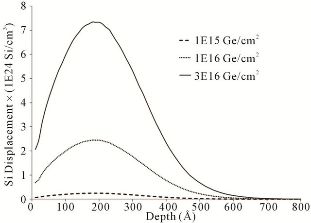
Figure 1. Monte Carlo Simulation of the induced damage of the 35 keV Ge implantation into the Si substrate using different doses of the Ge ions (1 × 10¹⁵, 1 × 10¹⁶, 3 × 10¹⁶ Ge+/cm2).
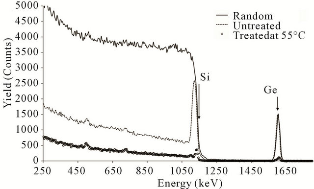
Figure 2. RBS spectra at both random (solid line) and channeling directions (hollow circles) for the Si implanted by 3 × 10¹⁶ Ge+/cm2 of 35 keV Ge ions without heat treatment (dash line) and after being annealed at 550˚C.
shows completely different scenario of the damage formation and heat-treated recovery of the crystal (hollow circles in Figure 2). From the RBS-C spectrum of the heat-treated sample, no remarkable peak and so no damage is visible in the energy range of 1100 keV equivalent to the surface of the Si substrate, confirms nearly full recovery of the damaged lattice of the Si substrate. Moreover, the Ge peak has been dropped considerably which is an indication of the effect of the annealing on the moving of the Ge interstitial atoms into the lattice sites of the Si substrate. This means the annealing temperature gives adequate energy to the interstitial Ge atoms to be able to overcome the crystal filed around lattice sites and occupy those lattice sites of the Si substrate.
In order to estimate the effect of the dose of the Ge impurity on the oxidation rate, we choose sample implanted by 3 × 10¹⁶ Ge+/cm2 at the energy of 35 keV to be wet oxidized at 900˚C for 10 minutes.
Since any defect at the interface or dissolving of the impurities into oxide layer can change the oxide’s morphology, the oxidation time and temperature have been chosen in order to get finally thin oxide layer for better analysis of the surface morphology. In addition, reduction of the effect of the amorphous oxide layer on the ion channeling for the purpose of damage study is another advantage of using thin layer of the oxide. Figure 3 compares RBS spectra of both implanted (hollow circles) and non-implanted (solid line) regions of the Si substrate after oxidation at the mentioned conditions. There was no pre-oxidation heat treatment to allow us just study the effect of the Ge impurity on the wet oxidation process. By looking at the Si edge of the RBS spectra, it clearly shows the considerable change of the oxide layer (energy range of 1050 to 1150 keV) for the implanted region, since this energy interval corresponds to the surface of the Si substrate being oxidized. The corresponding oxygen peaks, also, confirm such twice change in the thickness of the grown oxide layer. To extract quantitative
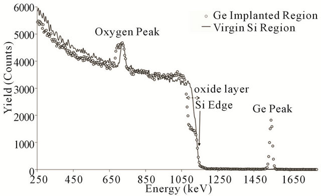
Figure 3. RBS spectra of the virgin silicon (solid line) and the implanted Si with 3 × 10¹⁶ Ge+/cm2 (open circles) oxidized at 900˚C for 10 minutes without pre-oxidation heat treatment.
information from the RBS spectra on the thickness, we run simulation using SIMNRA6.05 program as the common one in Ion Beam Simulation [11]. The results of the simulation get 440 Å and 1300 Å for the thicknesses of the oxide layers in the virgin and implanted regions, respectively. Such increasing in the rate of the oxidation due to the presence of the Ge impurity has been reported already at various oxidation conditions [3-5].
Now, by having rough estimation of the oxide thickness due to the presence of the Ge impurity, we try to assess the effect of the pre-oxidation annealing on the oxidation rate. On this purpose, the sample implanted with 1 × 10¹⁶ Ge+/cm2 dose of the doping is annealed at 500˚C N2 ambient for 30 minutes, but the oxidation conditions is kept like the one for the previous sample in Figure 3. To have a complete picture of the change of the oxidation rate, we also do oxidation for the virgin silicon and non-annealed samples at the same condition to avoid any change on the oxidation rate rising from variation of the time and temperature of the annealing process. RBS results in Figure 4 indicate the increase in the thickness of the silicon dioxide for the both implanted samples in compare with the virgin silicon being oxidized at the same condition (dash line). Running the simulation for the two implanted samples give the values of 711 Å for the thickness of the silicon dioxide for the sample both annealed and oxidized and 850 Å for the sample just oxidized. The thickness for the virgin silicon is 440 Å like the one in Figure 3. Therefore, the thickness of the oxide layers proves the effect of the pre-oxidation heating on the oxidation rate which is here slowing down the progressing of the oxidation rate after annealing. Also, as we expect [3-5], the Ge fluencies change the oxidation rate. The 1300 Å oxide layer of the 3 × 10¹⁶ Ge+/cm2 implantation dose gives the thicker silicon oxide than the 850 Å layer of the dose of 3 × 10¹⁶ Ge+/cm2 under the same oxidation conditions, but it
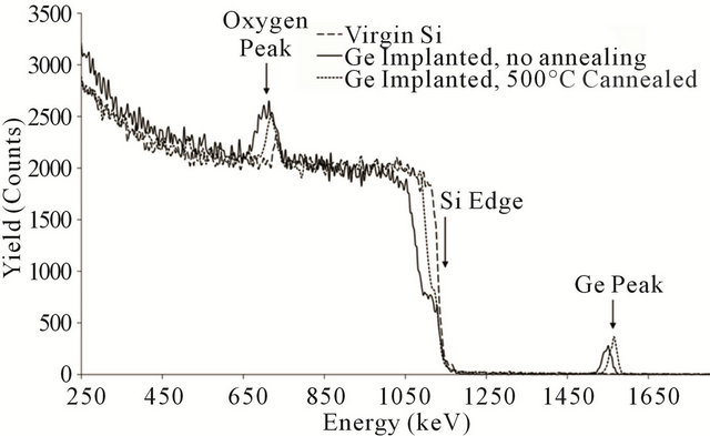
Figure 4. RBS spectra for the samples oxidized at 900˚C and implanted with 1 × 10¹⁶ Ge+/cm2 dose of Ge ions without annealing (solid line ), with annealing at 500˚C (dot line ) and without Ge impurity (dash line).
doesn’t follow the Deal-Grove model [1].
As the annealing temperature can force the Ge atoms to be randomly distributed in the Si lattice interstitial sites or occupies the Si lattice sites, we would like to investigate the role of the Ge redistribution after annealing on the oxidation process. The Ge peaks in Figure 4 for both implanted samples (treated and non-treated ones) are picturing the evolution of the Ge redistribution from non-treated (solid line) to the treated (dot-line) sample under the influence of the annealing. The height of the Ge peaks shows vividly the shrinking of the layer containing the Ge atoms for the sample being annealed before oxidation. Since in our RBS data, more height (more concentration) corresponds to the less thickness when we don’t have lost of the Ge atoms in the sample. In addition, the position of the Ge peak has shifted to the higher energy after annealing. Because the diffusion coefficient of the Ge into silicon oxide is less than that in silicon itself [12,13], and no one has reported the trace of the Ge ions at the oxide layer after wet oxidation during 10 minutes, we expect no Ge ions at the oxide side of the interface. Our RBS spectra, also, do not show any sudden or gradual broadening in the higher energy edge of the Ge peak (Figure 4); hence progressing the oxide layer into the silicon substrate has been resulted in the pile up of the Ge ions at the interface. The width of the Ge peaks would approve the formation of the thinner layer of the germanium since the width of the Ge peak in the treated sample has been reduced after thermal treatment with regards to the peak of the non-treated sample. Consequently, the behavior of the annealed sample implies that the Ge redistribution can be really effective in the oxidation process and can be used to control the composition and the thickness of the formed SixGe1−x layer.
The overall assessment of the experiments being reported here highlights the role of the Ge redistribution on the oxidation rate and thereafter, the formation of the SixGe1−x layer. In the non-treated sample like the one in
Figure 3 (open circles) which we don’t have the significant reduction in the height of the Ge peak owing to much less lattice substitution of the Ge atoms, we obtain higher oxidation thickness and rate. Thus the occupation of the interstitial sites of the Si lattice by the Ge atoms increases the oxidation rate; however it gives rise to the thicker layer of the formed SixGe1−x as we discussed in Figure 4 for the non-treated sample. On the contrary, the annealing process pushes the Ge atoms into the thinner layer of the SixGe1 − x at the interface while these Ge atoms have been substituted into the Si lattice sites and this substitution facilitates bonding of the Ge ions with the Si atoms [12]. In addition, the Ge atoms with bigger radius size being substituted into the Si lattice sites can induce stress/strain at the interface of the Si/oxide. The RBS-C spectrum of the treated sample in Figure 2 reveals the dechannling effect as an indication of having some stress/strain in the SiGe layer at the interface which can affect the oxidation rate. (Otherwise we expect much reduction in RBS-C yield like the virgin Si)
Due to the afterward steps on the grown silicon dioxide important for the Si industries, we have to study the roughness evolution of the oxide surface by variation of the dose of the implantation and annealing temperature. AFM images of the surface of the oxide for the samples oxidized without annealing ( upper part) and the ones oxidized with pre-annealing at the temperature range of 500˚C to 550˚C ( lower part) have been shown in Figure 5. As it can be seen, all images of the non-treated samples Figures 5(a)-(c) show more roughness than the treated ones Figures 5(d)-(f) which implies the effect of the pre-oxidation heat treatment on the improving of the surface roughness of the silicon dioxide.
Table 1 reports our roughness related parameters calculated using the SPIP6.0.3 [14] software for all the samples. Before doing calculation, all images have been plane corrected and then the analysis was done on whole image (512 × 512 pixels), which for some images, the contamination originated during the oxidation process may change slightly the results. However, the 2D images of the Figure 5 indicates only 1 or 2 particles with small sizes which they do not affect total analysis of the images. In Table 1, Sa and Sq are two common parameters used to refer to the roughness values, the first one shows the average and the second one the RMS values for the surface [15]. The RMS values reveal the trend of the increasing roughness by increasing the dose of the implantation which is expected due to the more accumulation of the damages and impurities at the interface. However, this trend is revered when it goes from 1 × 10¹⁶ to 3 × 10¹⁶ Ge+/cm2 owing to the more oxidation thickness which suppresses the effect of the interface roughness on the roughness of the oxide’s surface.
The RMS values for the treated samples show the better roughness values for the two first implantation doses (1 × 10¹⁵ and 1 × 10¹⁶ Ge+/cm2), but for the higher implantation dose, the pre-heating increases the roughness. We already showed that the annealing process before oxidation reduces the oxide thickness, so we expect the oxide’s surface to be affected more by the roughness of the interface for high implantation dose. The roughness of the interface is the result of uncompleted damage recovery during annealing due to higher amount of the Ge ions and so the accumulation of the some Ge atoms at the interstitial places in the Si lattice at the interface. But, for lower implantation doses, the annealing gives rise to the better recovery and so better substitution of the Ge impurities into the Si lattice sites. Therefore, we have less roughness at the interface and then the surface which we
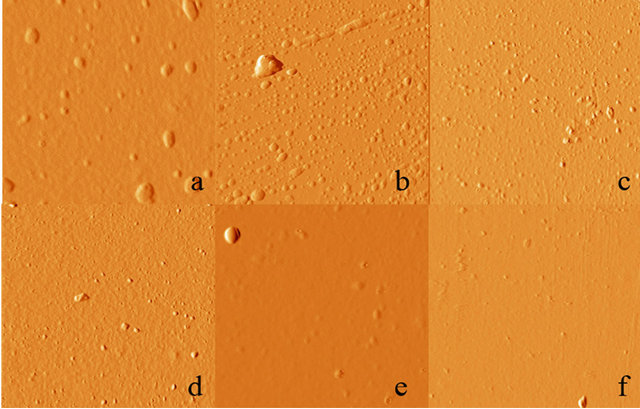
Figure 5. 2-D AFM images of the samples oxidized without heat-treatment: (a) 1 × 10¹⁵ Ge+/cm2, (b) 1 × 10¹⁶ Ge+/cm2, (c) 3 × 10¹⁶ Ge+/cm2 and with heat-treatment, (d) 1 × 10¹⁵ Ge+/cm2, (e) 1 × 10¹⁶ Ge+/cm2, (f) 3 × 10¹⁶ Ge+/cm2.
Table 1. The results of the calculation done using SPIP6.0.3 software on the AFM images in the scan area of 3 µm × 3 µm to compare the roughness parameters of the treated and non-treated samples.
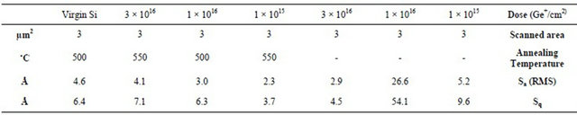
can visibly see it in the RMS results of the annealed samples for the first two doses.
4. Conclusion
RBS spectroscopy in Random and Channeling modes and AFM analysis have been carried out to show that there is different regime of the oxidation and resulting surface topology using pre-oxidation annealing, all been affected by Ge redistribution and crystal recovery. Our results confirmed that both Ge lattice site location and the induced strain/stress in the Si lattice at the interface can change the oxidation process, although we are not able to discriminate the role of each one separately. Since these two parameters are strongly dependent on the annealing process, by choosing the proper annealing conditions with regards to the Ge fluencies, we can tune the oxide thickness and the morphology of the surface. However, the formation of the epitaxial layer of the Si and Ge should be traced using transmission electron microscopy as the next phase of our research to understand the best quality of the interface between oxidized samples with and without annealing.
5. Acknowledgements
The authors would like to acknowledge the support of the Islamic Azad University, Ardabil Branch under the project number 278.
REFERENCES
- B. E. Deala and A. S. Grove, “General Relationship for the Thermal Oxidation of Silicon,” Journal of Applied Physics, Vol. 36, No 12, 1965, pp. 3770-3778. doi:10.1063/1.1713945
- C. P. Ho and J. D. Plummer, “Si / SiO2 Interface Oxidation Kinetics: A Physical Model for the Influence of High Substrate Doping Levels I. Theory,” Journal of Electrochemical Society, Vol. 126, No. 9, 1979, pp. 1516-1522. doi:10.1149/1.2129320
- A. Terasi, S. Scalese, M. Re, E. Rimini and F. Lacona, “Thermal Oxidation of Si(100) Single Crystal Implanted with Ge Ions,” Journal of Applied Physics, Vol. 91, No. 10, 2002, pp. 6754-6761. doi:10.1063/1.1471942
- K. Hossain, L. KSavage and O. W. Holland, “Rate Enhancement during Thermal Oxidation of Ge+-Implanted Si,” Nuclear Instrument and Methods in Physics Research B, Vol. 241, No. 1-4, 2005, pp. 553-558. doi:10.1016/j.nimb.2005.07.103
- K. Hossain, O. W. Holland, F. U. Naab, R. Poudel and J. L. Duggan, “Dose-Dependent Thermal Oxidation of Ge+- Implanted Silicon,” Nuclear Instrument and Methods in Physics Research B, Vol. 261, No. 1-2, 2007, pp. 620-623. doi:10.1016/j.nimb.2007.04.240
- S. N. Dedyulin and L. V. Goncharova, “Thermal Oxidation of Ge-Implanted Si: Role of Defects,” Nuclear Instruments and Methods in Physics Research B, Vol. 272, 2012, pp. 334-337. doi:10.1016/j.nimb.2011.01.095
- A. Baghizadeh, D. Agha-Aligol, D. Fathy, M. LamehiRachti and
 M. Moradi, “Formation of As Enriched Layer by Steam Oxidation of As+-Implanted Si,” Applied Surface Science, Vol. 255, No. 11, 2009, pp. 5857-5860. doi:10.1016/j.apsusc.2009.01.021
 - J. F. Ziegler, M. D. Ziegler and J. P. Biersack, “SRIM— The Stopping and Range of Ions in Matter (2010),” Nuclear Instruments and Methods in Physics Research Section B, Vol. 268, No. 11-12, 2010, pp. 1818-1823. doi:10.1016/j.nimb.2010.02.091
- C. Cohen and D. Dauvergne, “High Energy Ion Channeling: Principles and Typical Applications,” Nuclear Instrument and Methods in Physics Research B, Vol. 225, No. 1-2, 2004, pp. 40-71. doi:10.1016/j.nimb.2004.03.017
- F. Sánchez-Almazán, E. Napolitani, A. Carnera, A. V. Drigo, M. Berti, J. Stangl, Z. Zhong, G. Bauer, G. Isella and H. von Känel, “Ge Quantification of High Ge Content Relaxed Buffer Layers by RBS and SIMS,” Nuclear Instrument and Methods in Physics Research B, Vol. 266, 2004, pp. 301-308. doi:10.1016/S0168-583X(04)00833-X
- M. Mayer, “SIMNRA, a Simulation Program for the Analysis of NRA, RBS and ERDA,” American Institute of Physics Conference Proceedings, Vol. 475, 1999, pp. 541-544.
- S. M. Sze, “VLSI Technology,” 2nd Edition, Mc GrawHill Book, New York, 1983.
- H. G. Chew, W. K. Choi, Y. L. Foo, W. K. Chim, E. A. Fitzgerald, F. Zheng, S. K. Samanta, Z. J. Voon and K. C. Seow, “TEM Study on the Evolution of Ge Nanocrystals in Si Oxide Matrix as a Function of Ge Concentration and the Si Reduction Process,” Advanced Materials for Microand Nano-Systems (AMMNS), 2006. http://hdl.handle.net/1721.1/29824
- SPIP6.0.3. http://www.imagemet.com/index.php
- A. Terrasi, E. Rimini, V. Raineri, F. Iacona, F. La Via, S. Colonna and S. Mobilio, “Precipitation of As in Thermally Oxidized Ion-Implanted Si Crystals,” Applied Physics Letters, Vol. 73, No. 18, 1998, pp. 2633-2635. doi:10.1063/1.122536