Smart Grid and Renewable Energy
Vol. 4 No. 1 (2013) , Article ID: 28142 , 9 pages DOI:10.4236/sgre.2013.41014
Parasitic Effects on the Performance of DC-DC SEPIC in Photovoltaic Maximum Power Point Tracking Applications
![]()
1Department of Electrical & Electronic Engineering, Chittagong University of Engineering & Technology, Chittagong, Bangladesh; 2Department of Electrical & Electronic Engineering, Bangladesh University of Engineering & Technology, Dhaka, Bangladesh.
Email: nureee_ruet@yahoo.com
Received November 8th, 2012; revised December 8th, 2012; accepted December 15th, 2012
Keywords: Photovoltaic (PV) Renewable Energy Systems; DC-DC Converter; Parasitic Resistance; Maximum Power Point Tracking (MPPT); Single Ended Primary Inductance Converter (SEPIC)
ABSTRACT
This paper presents an analysis of the effect of parasitic resistances on the performance of DC-DC Single Ended Primary Inductor Converter (SEPIC) in photovoltaic maximum power point tracking (MPPT) applications. The energy storage elements incorporated in the SEPIC converter possess parasitic resistances. Although ideal components significantly simplifies model development, but neglecting the parasitic effects in models may sometimes lead to failure in predicting first scale stability and actual performance. Therefore, the effects of parasitics have been taken into consideration for improving the model accuracy, stability, robustness and dynamic performance analysis of the converter. Detail mathematical model of SEPIC converter including inductive parasitic has been developed. The performance of the converter in tracking MPP at different irradiance levels has been analyzed for variation in parasitic resistance. The converter efficiency has been found above 83% for insolation level of 600 W/m2 when the parasitic resistance in the energy storage element has been ignored. However, as the parasitic resistance of both of the inductor has increased to 1 ohm, a fraction of the power managed by the converter has dissipated; as a result the efficiency of the converter has reduced to 78% for the same insolation profile. Although the increasing value of the parasitic has assisted the converter to converge quickly to reach the maximum power point. Furthermore it has also been observed that the peak to peak load current ripple is reduced. The obtained simulation results have validated the competent of the MPPT converter model.
1. Introduction
The Photovoltaic (PV) energy is one of the promising alternative renewable energy resources that can be used to minimize the existing electricity crisis in the world considerably. PV energy is getting increasing importance as a renewable source due to the advantages such as the absence of fuel cost, little maintenance, no carbon emission at all and no noise due to absence of moving parts. The output current vs. voltage curve of PV array shows a non-linear I-V characteristic that depends on environmental conditions such as solar irradiance and temperature. In this curve, there is a certain operating point at which the PV array produces maximum power which is known as maximum power point (MPP). Therefore, to maximize the PV array output power at any irradiance and temperature, maximum power point tracking (MPPT) is used in the PV system. The maximum power theory is based on impedance matching. By adjusting the duty cycle of the converter, the equivalent load impedance as seen by the PV source is matched with its own impedance. Using an appropriate MPPT algorithm, the duty cycle of the converter is adjusted continuously to track the MPP. The MPPT scheme using the basic switch mode converter topologies have their own advantages and disadvantages. The main requirement of any converter used in the MPPT system is that it should have a low input current ripple. Buck or its derived topologies give pulsating currents on the PV array side. On the other hand, as compared with buck topologies, the boost or its derived topologies present low current ripple on the PV side, but high ripple in the load current. The requirement of load voltage, either lower or higher than the array voltage, can be realized by means of buck-boost converters. But, still the PV array current and load current are pulsating in nature. Furthermore, load voltage is inverted with buck-boost converter. These aforementioned restrictions of the conventional converters have motivated researchers and system designers to investigate the feasibility of employing single switch fourth order converters, namely single-ended primary inductance converter (SEPIC) [1-3], Cuk converter [4-9] and Zeta converter [10,11] to provide alternative solution. The term fourth order means these converters have four energy storage elements—two inductors and two capacitors to transfer energy from input side to output side. In general, these fourth order converters have wide range of input-tooutput conversion ratio, better adaptability of integrating transformers for galvanic isolation, and non-pulsating input and output current. For example SEPIC converter provides the buck-boost conversion function without polarity reversal unlike buck-boost, in addition to the low ripple input current. The authors in [12,13] have suggested that SEPIC topology is highly suitable for multiple-input DC-DC converter because of its non-pulsating input current, grounded switch and non-inverting output voltages. SEPIC may also be preferred for battery charging systems because the diode placed on the output stage works as a blocking diode preventing a reverse current going to PV source from the battery [14]. Additionally, the Electromagnetic Interference (EMI) behavior of a SEPIC topology is much better than a step-down or flyback topology and avoids the problems with leakage inductance and snubbers [15]. The inductor used in the SEPIC has a certain amount of non-zero dc parasitic resistance, as it is usually a winding of several turns of long metallic wire. Similarly, the capacitor has also a small equivalent series parasitic resistance. But the parasitic resistance of capacitor may be neglected comparing to that of inductor may be neglected without loss of generality [16]. Apart from adding ohmic losses, these parasitic resistances add current damping and affect the ripple attenuation [17]. Although considering ideal components significantly simplifies model development, but neglecting the parasitic effects in models may sometimes lead to failure in predicting the fast-scale instabilities [18]. Therefore, it is important to take the effects of parasitics into consideration for improving the efficiency, dynamic performance, stability and robustness of the converter. In case of SEPIC converter used for MPPT applications, a detail investigation is necessary to observe and analyze the effects of parasitics on the overall performance of the converter which is still not reported in the literature. In this paper, the effects of these parasitic resistances on the overall performance of these converters especially in MPPT applications are analyzed.
2. PV Array Characteristics
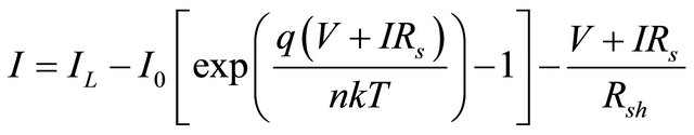
An ideal solar cell may be modeled by a current source connected in parallel with a diode; the current source represents the generated photocurrent when the sunlight hits the solar panel, and the diode represents the p-n transition area of the solar cell. In practice no solar cell is ideal and a shunt resistance  and a series resistance
  component are incorporated in the model according to its behavior. The equivalent circuit of solar cell comprising desecrates components is shown in Figure 1.
From the above electrical equivalent circuit of solar cell, it is evident that the  is the voltage across the load resistance
  and the current
  which is flowing through this load can be written as Equation (1).
 (1)
(1)
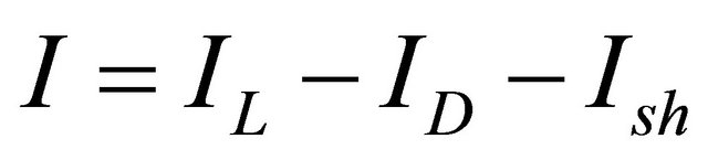
where IL light generated current, ID is the diode current Ish is the current which is shunted through Rsh.
By the Shockley diode Equation [19], the current diverted through the diode is given by Equation (2).
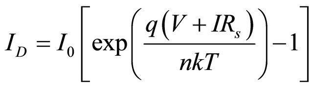 (2)
(2)
Here ![]() is the absolute temperature in Kelvin.
is the absolute temperature in Kelvin.  is the charge of a electron,
  is the Boltzmann’s constant,
 ![]() is the diode ideality factor which depends on the certain PV technology and
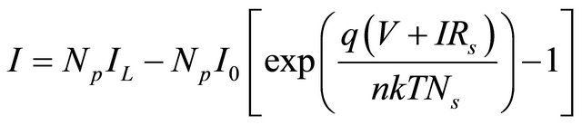
is the diode ideality factor which depends on the certain PV technology and  is the reverse saturation current in amperes. Substituting these into the Equation (1), produces the characteristic Equation (3), of a typical solar cell, this relates solar cell parameters to the output current and voltage.
 (3)
(3)
Sometimes, to simplify the model, the effect of the shunt resistance is not considered, that is  is infinite, so the expression of (3), simplify to as Equation (4).
 (4)
(4)
A PV panel is composed of many solar cells, which are connected in series and/or parallel so the output current and voltage of the PV panel are high enough for a certain application. Taking into account the simplification of Equation (4), the output current-voltage characteristic of a PV panel is expressed by Equation (5), where,  and
and  are the number of solar cells in parallel and series respectively.
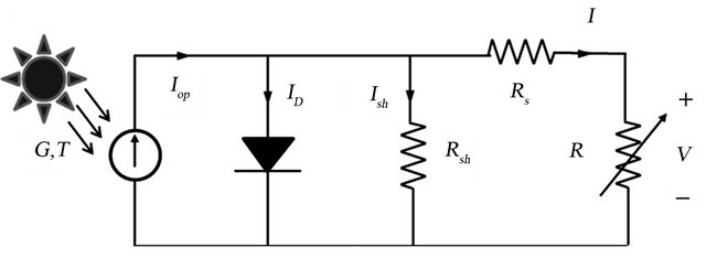
Figure 1. Equivalent circuit of a solar cell.
 (5)
(5)
The intensity of solar irradiance (insolation) is the most dominant environmental factor which is strongly affecting the electrical characteristics of solar panel according to the Equation (5). The effect of the irradiance on the voltage-current (V-I) and voltage-power (V-P) characteristics of STF100P6 solar panel under various irradiances level is best depicted in Figure 2. From this Figure it is clear that under higher irradiance, the PV cell produces higher output currents because the light generated current is proportionally generated by the flux of photons.
The maximum power point (MPP) decreases with decreasing irradiance and this is indicated on each (V-P) curve in Figure 3.
3. Maximum Power Point Tracking (MPPT)
Usually there are two major approaches adopted for maximizing power extraction from PV sources. First one is the mechanical tracking of the solar panel. In this case the panel is attempted to position in any terrain at an an-
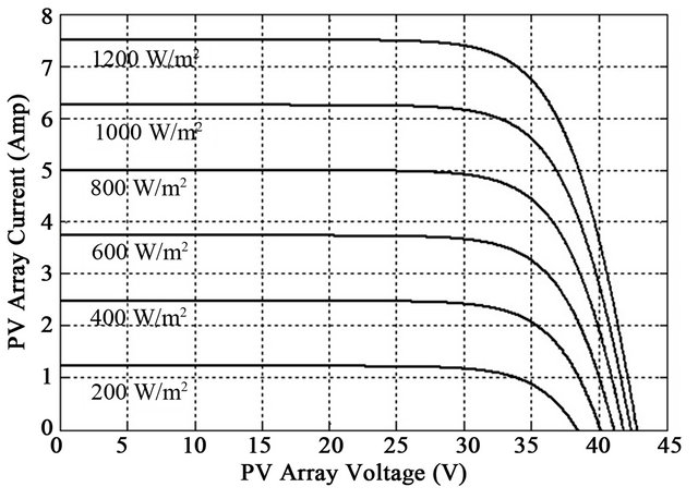
Figure 2. I-V characteristics of the solar PV array due to change in insolation at 25˚C.
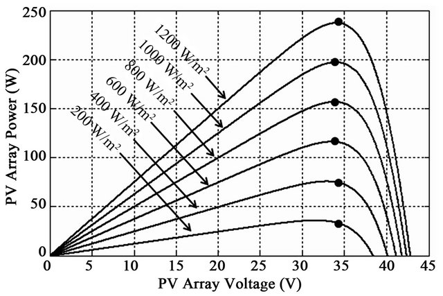
Figure 3. P-V characteristics of the solar PV array due to change in insolation at 25˚C.
gle of ninety degree with the direction incoming ray of sun. This issue is beyond our topic of discussion. The second one is the electrical MPPT where electrical operating point is forced at the peak power point continuously by adjusting the duty cycle of the DC-DC converter inserted between PV array and load. However several MPPT methods have been summarized in the literatures [20,21]. The methods vary in complexity, sensors required, tracking efficiency, convergence speed, cost, and in other respects. Some of the well-known techniques are Perturb & Observe (P & O), Incremental Conductance, Fractional Open-Circuit, Fractional Short-Circuit, Fuzzy Logic and Neural Network based algorithms. Among them the Perturb and Observe (P & O) algorithm is most commonly used in practice due to its fast tracking speed, low cost and eases of implementation by the majority of authors [22-27]. It is an iterative method of obtaining MPP. It measures the PV array voltage and current, and then perturbs the operating point of PV generator to encounter the change direction. The maximum point is reached when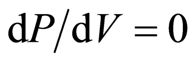 . There are many varieties, from simple to complex. But the most basic form explained in Figure 4; that has been adopted in this paper. To seek MPP, the operating voltage of the PV array perturbed, by a small amount,
  and the resulting change in power,
  is measured. If the power increases due to the perturbation then the next perturbation of the operating voltage is continued in the same direction. However, if the power decreases, the subsequent perturbation should be reversed.
The process is repeated until the MPP is reached. The system may oscillates about the MPP if the meteorological conditions change abruptly. But in reality insolation and temperature has slower dynamics and never gives a big jump in a very short time. A summary of the algorithm is presented in Table 1.
4. Operation and Modeling of SEPIC
The single-ended primary-inductor converter (SEPIC) as indicated in the MPPT implementation circuit of Figure 5 has the ability to operate from an input voltage that is
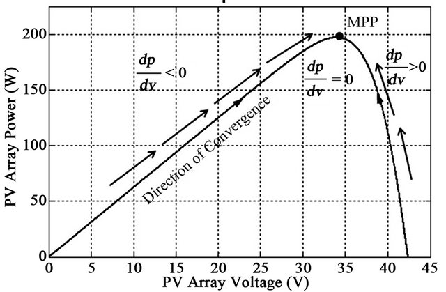
Figure 4. Maximum power point tracking technique.
Table 1. Summary of perturb and observe algorithm.
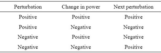
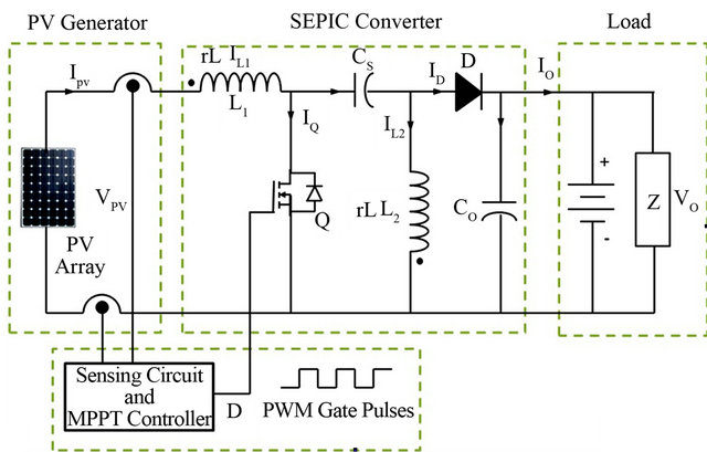
Figure 5. MPPT implementation circuit using SEPIC.
greater or less than the regulated output voltage without polarity reversal. Aside from being able to function as both a buck and boost, its minimal current ripple improves average value of current and voltage as well. The converter exchanges energy between the capacitors and inductors in order to convert from one level of voltage to another. The primary means of transfer energy from the input to the output of the converter is through a series capacitor which is known as SEPIC capacitor or coupling capacitor, .
.
The voltage rating of this capacitor must be greater than the maximum input voltage. The output voltage is controlled by adjusting duty cycle of control switch, . The control switch is typically a MOSFET, which offer much higher input impedance and lower voltage drop and do not require biasing resistors. The first input inductor
  together with the MOSFET control switch resembles a simple boost topology, whereas the shunt inductor
 , location is similar to a buck-boost topology. The Diode,
  should have fast recovery time and low forward-voltage drop. Its peak current rating is greater than or equal to the peak inductor current and reverse breakdown voltage must be greater than the output voltage. When the control switch is turned on, diode is turn off and the output current is solely supplied by the output capacitor,
 . Thus the selected output capacitor must be capable of handling the maximum rms current. To understand the voltages at the various nodes and current through different branches, the circuit is assumed in an average state with continuous conduction mode. The initial state of a SEPIC before the switch closes is shown in Figure 6(a). The coupling capacitor has charged to
 . The output voltage is zero, and no current is flowing in any of the components. When the switch closes as shown in Figure 6(b),
  is applied across the first inductor and current, iL1 ramps up through it.
The voltage,  across the coupling capacitor is also applied across the second inductor
  and current
  ramps up through it in similar way that of
 . The diode is reverse biased and the output capacitor is left to provide the load current in this time. The fact that when the switch is on, both
  and
and  are charged up and disconnected from the load and both the capacitors discharge.
The associated voltage across the inductor  and the diode
  as well as the instantaneous current through each components of the converter are best sketched in Figure 7. When the switch is off, the current through
  has no place to go but through the
  to the load as the diode is forward biased. The current through shunt inductor
  must also go to the output. Both inductors provide current to the load capacitor and load. This switching state of the converter circuit is shown in Figure 6(c). In order for the current to continue to flow through
 , the voltage on the switch boosts up to
 . The current flowing through the capacitor
  charges it up in this time to enable it to transfer this energy to shunt inductor
  until the switch closes again for the next cycle. There is an energy balance between the coupling capacitor
  and shunt inductor
 , which helps determine the value of the capacitor
 . As the capacitor
  blocks direct current and hence the average current through it is zero, making inductor
  the only source of load current. Therefore, the average current through inductor
  is the same as the average
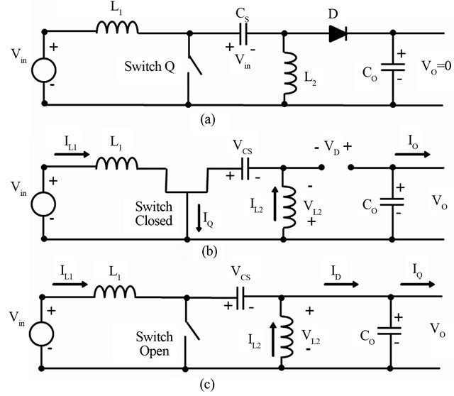
Figure 6. SEPIC circuit state (a) Before switch is on; (b) When switch on; and (c) When switch off.
Figure 7. Voltages and current of each component of the SEPIC in CCM.
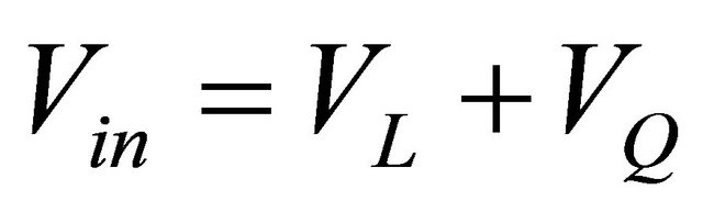
load current and hence independent of the input voltage. Looking at average voltages across  which is actually zero for a full cycle, the energy balance volts-hertz [28] equation can be written as:
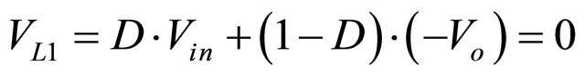 (6)
(6)
 (7)
(7)
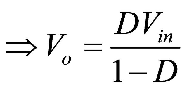
For ideal converter
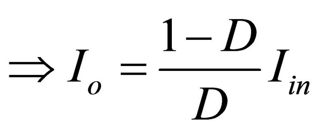 (8)
(8)
The above voltage and current relation prove that the SEPIC has the ability to operate from an input voltage that is greater or less than the regulated output voltage without polarity reversal unlike the conventional buck bust converter.
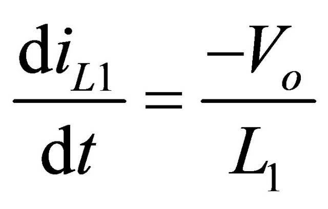
4.1. Determining Peak Inductor Current
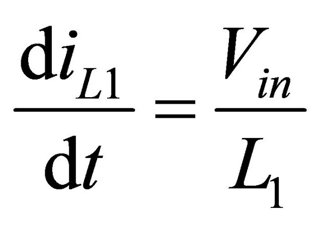
The graph of  is shown in Figure 8. For PV applications, it is desired to have low ripple in
  to keep the solar panel operating at its MPP. At discharging phase of inductor,
  can be written as:
 (9)
(9)
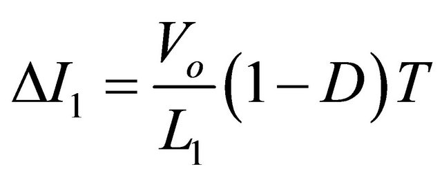 (10)
(10)
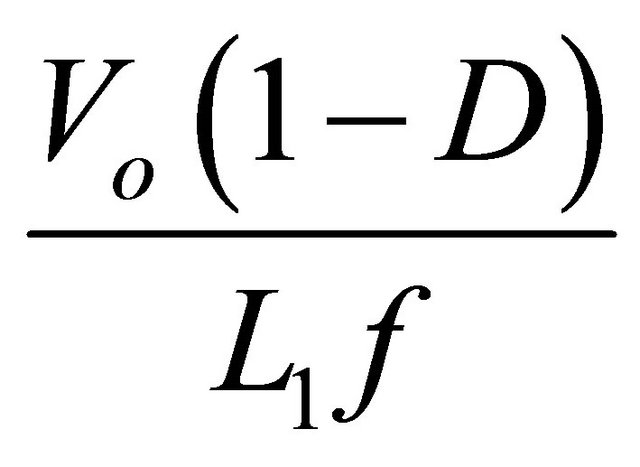 (11)
(11)
4.2. Determining Peak Inductor Current
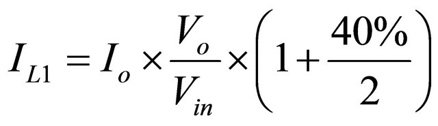
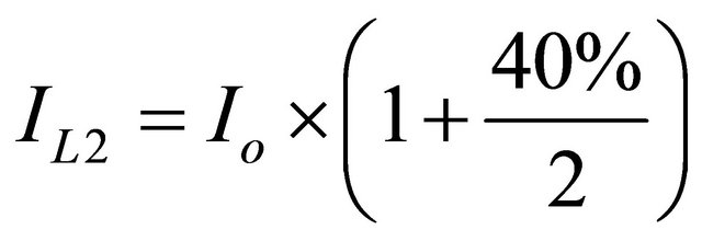
One of the first steps in designing any PWM switching regulator is to decide how much inductor ripple current,  , to allow. Too much increases EMI, while too little may result in unstable PWM operation. A good rule for determining the inductance is to allow the peak-to-peak ripple current to be approximately 40% of the maximum input current at the minimum input voltage [29]. The ripple current flowing in equal value inductors
  and
and  is given by:
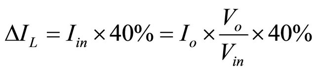
The value of the first inductor  is derived from the following fundamental relation of
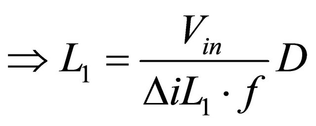 (12)
(12)
Similarly the value of the inductor  is derived from the following fundamental relation of
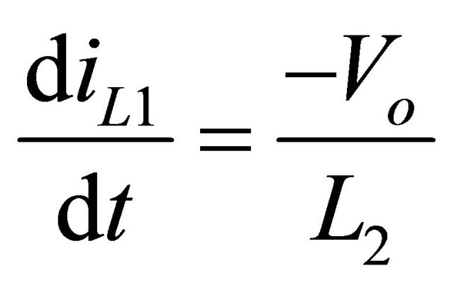 (13)
(13)
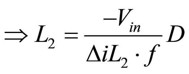 (14)
(14)
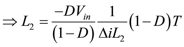
Ignoring the sign from Equation (12) and Equation (14) and considering the magnitude of current ripple 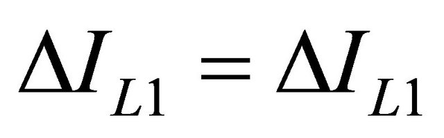 , it can be said that,
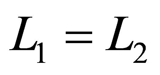 . That is, both the inductors have to have same level of inductance. It proves that they have induced same level of voltage with opposite polarity. Physically the windings are constructed with the same number of turns on the similar ferrite iron core. To ensure the inductor does not saturate, the peak current in the inductor is given [30] by:
 (15)
(15)
 (16)
(16)
5. Dynamic Performance Analysis
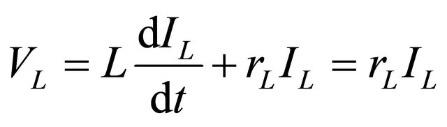
For the sake of simplicity, we consider here that the inductor is the only non-ideal component, and that it is equivalent to an inductor and a resistor in series. This assumption is acceptable because an inductor is made of one long wound piece of wire, so it is likely to exhibit a non-negligible parasitic resistance ( ). Furthermore, current flows through the inductor both in the on and the off states in continuous conduction mode of operation. Using the state-space averaging method, we can write:
 (17)
(17)
where  and
and  are respectively the average voltage across both of the inductor. If we consider that the converter operates in steady-state, the average current through the inductor is constant [31]. The average voltage across the inductor is:
 (18)
(18)
When the switch is in the on-state,  and when it is off, the diode is forward biased. Therefore,
  So, the average voltage across the switch is:
 (19)
(19)
The average inductor current in terms of average output current is:
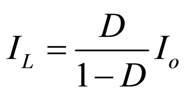 (20)
(20)
Assuming the output current and voltage have negligible ripple. For the purely resistive load of  Equation (28) becomes:
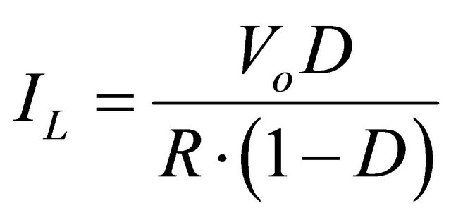 (21)
(21)
Using the previous equations, the input voltage becomes:
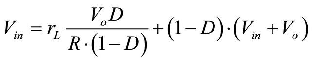 (22)
(22)
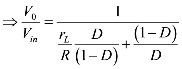 (23)
(23)
If the  is zero, Equation (23) represents the ideal case. However, as
  increases, the voltage gain of the converter decreases. The effect of
  increases with the increase of duty cycle which is displayed graphically in Figure 9. As the inductor becomes less ideal, the possible gain drops off sharply from the theoretical value, especially as the duty cycle increases above 90%. The normal operating cell temperature (NOCT) rating of 48˚C was assumed throughout the simulation. Only the change of intensity of solar irradiation is taken into consideration. The complete model of the proposed system in MATLAB/SIMULINK [32] environment is given in Figure 10. Specification of PV module [33] and converter parameters are optimized and calculated values are summarized in Table 2.
The voltage and power in the output of the converter for the case of ideal inductor SEPIC and when the inductor parasitic resistance is not taken into consideration is shown in Figures 11-14, respectively. In Figure 11, it has been
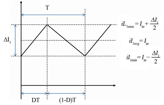
Figure 8. Inductor current waveform for CCM.
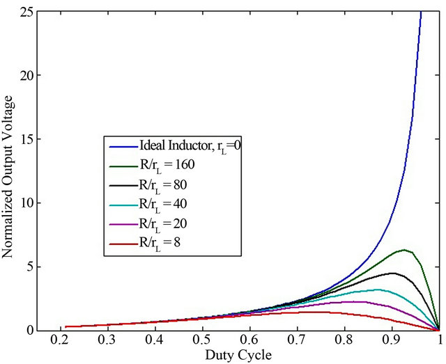
Figure 9. Normalized voltage of SEPIC with the duty cycle when the parasitic resistance of inductor varies.
Table 2. Specification of PV module and converter ratings.
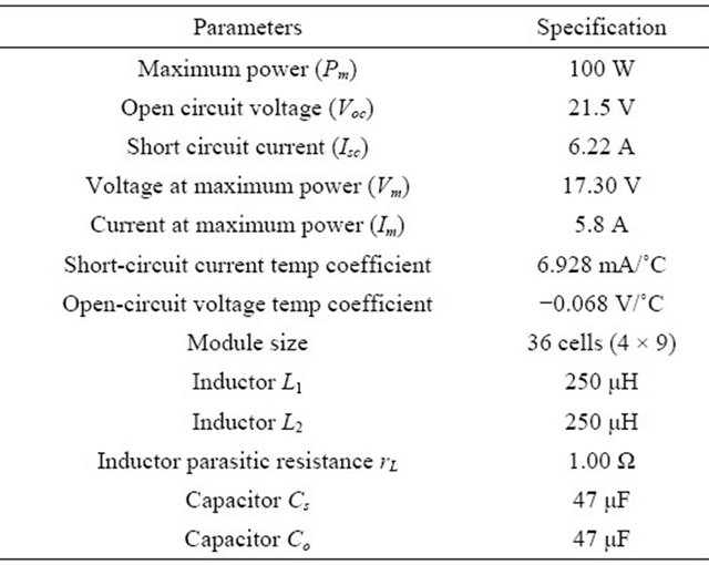
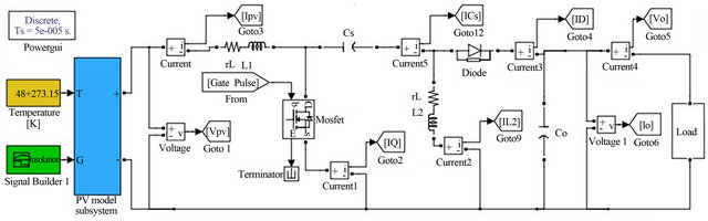
Figure 10. The detailed simulink model of SEPIC based MPPT system.
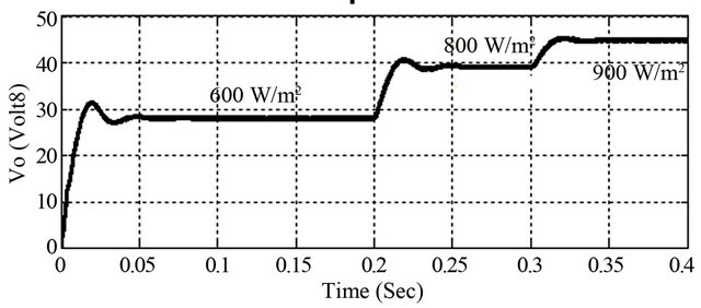
Figure 11. Higher output voltage swing for step up change of insolation for ideal inductor.
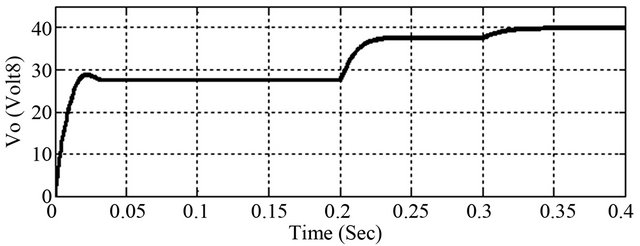
Figure 12. Reduced output voltage swing for the presence of inductor parasitic resistance.
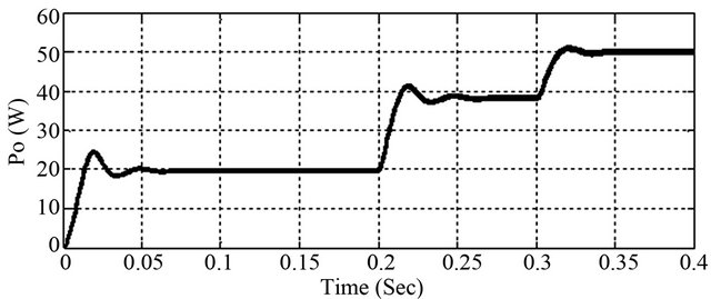
Figure 13. Output power for step up change of insolation for ideal inductor.
observed that voltage get back its stable level at 28 V, 39 V and 45 V for insolation step of 600 W/m2, 800 W/m2 and 900 W/m2 respectively after some considerable delay.
The respective maximum power levels are shown in Figure 13 has stable in 20 W, 38 W and 50 W accordingly. This happens because the algorithm provides the optimum duty ratio perturbation as the PV arrays are very
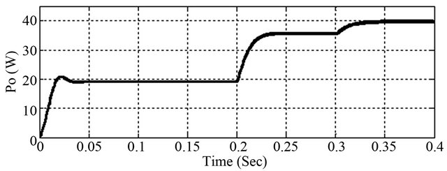
Figure 14. Parasitic resistance assists to converge MPPT.
sensitive to rapid environmental changes. Similar phenomena are observed in Figure 12, but here change of voltage swing is relatively less before get back its stable position. The variations in the voltage and power of the converter are almost terminated when the solar radiation is almost constant. For example this can be seen between 0.05 sec. and 0.2 sec. in the time scale. The converter efficiency has been found more than 83% for insolation level of 600 W/m2. It’s stable at 28 V, 38 V and 40 V for insolation level of 600 W/m2 800 W/m2 and 900 W/m2 respectively. For the same level of last two insolation profile as taken into consider for first the case it has been found that 5% and 15% less than the previous on due to effect of parasitic of inductor. The respective power levels are shown in Figure 14, which are stabled at 20 W, 38 W and 50 W. The variations in the voltage and power of the converter are almost terminated when the solar radiation is almost constant but in this case both of these get back its stability very quickly for inductor damping. For example this can be seen between 0.03 sec. and 0.2 sec. in the time scale. However the converter efficiency has been found less than 78% for insolation level of 600 W/m2. The output current for step down change of insolation profile of 1000 W/m2, 850 W/m2 and 700 W/m2 for ideal inductor as well as when the effect of inductor parasitic resistance is considered is shown in Figures 15 and 16 respectively.
It is clear from these figures that the average value of output current is reduced to 17.54% for the presence of 1 ohm parasitic resistance in the energy storage element.
The effect of parasitic in current ripple is presented in Figures 17 and 18. The calculated value of the peak to peak output current ripple is 5 mA when the parasitic resistance has been ignored. The average value of output current is 1.24 A. On the other hand, the peak to peak output current ripple is 4 mA when the parasitic resistance of 1 ohm has been considered and the average value of output current is reduced to 1.0225 A. This is due to account for adding ohmic losses of parasitic elements. Apart from adding ohmic losses these resistances add current damping and affect the ripple attenuation as well.
6. Conclusion
The effects of parasitics on the overall performance of the converter have been analyzed in this paper and have been found that the inductor parasitic resistances have large effects on the converter efficiency and ripple. Firstly both of the two inductors are assumed ideal and hence power is transmitted with fewer losses from the input side to the load. The loss which has been encounter was due to the switching loss of the converter. The converter efficiency has been found above 83% for insoletion level of 600 W/m2 in this case. However, as  increases, the pos-

Figure 15. Output current for step down change of insoletion for ideal inductor.
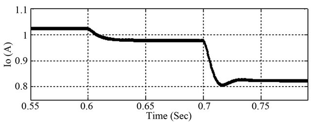
Figure 16. Consequence of inductor parasitic resistance on output current.
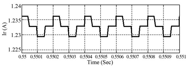
Figure 17. Output current ripple for ideal inductor.
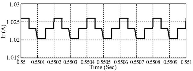
Figure 18. Consequence of parasitic resistance on output current ripple.
sible gain drops off sharply from the theoretical value, especially as the optimum duty cycle of around 90%. A fraction of the power managed by the converter is dissipated by these parasitic resistances. The voltage as well as current gain of the converter decreases compared to the ideal case. The converter efficiency has been found less than 78% for the insolation level of 600 W/m2. So Inductors with lower series resistance allow less energy to be dissipated as heat, resulting in greater efficiency and a larger portion of the input power being transferred to the load.
7. Acknowledgements
This work has been supported partially by the post graduate research grant of the Chittagong University of Engineering & Technology (CUET), Bangladesh. I also express my gratitude to my honorable teacher, Muhammad Quamruzzaman, Assistant Professor, Department of Electrical & Electronic Engineering, who gave me inspiration, cordially guidance, and valuable suggestions which helped me to complete my research work.
REFERENCES
- M. Veerachary, “Power Tracking for Nonlinear PV Sources with Coupled Inductor SEPIC Converter,” IEEE Transactions on Aerospace and Electronic Systems, Vol. 41, No. 3, 2005, pp. 1019-1029. doi:10.1109/TAES.2005.1541446
- J. Hu, A. D. Sagneri, J. M. Rivas, Y. Han and D. J. Perreault, “High-Frequency Resonant SEPIC Converter with Wide Input and Output Voltage Ranges,” IEEE Transactions on Power Electronics, Vol. 27, No. 1, 2012, pp. 189- 200. doi:10.1109/TPEL.2011.2149543
- S. B. Kjaer, J. K. Pdersen and F. Blaabjerg, “Modeling and Control of PV Charger System with SEPIC Converter,” IEEE Transactions on Industrial Electronics, Vol. 56, No. 11, 2009, pp. 4344-4353. doi:10.1109/TIE.2008.2005144
- R. M. Middlebrook and S. Cuk, “A General Unified Approach to Modeling Switching Converter Power Stages,” Proceedings of IEEE Power Electronical Special Conference, Vol. 4, 1976, pp. 18-34.
- A. Safari and S. Mekhilef, “Simulation and Hardware Implementation of Incremental Conductance MPPT with Direct Control Method Using Cuk Converter,” IEEE Transactions on Industrial Electronics, Vol. 58, No. 4, 2011, pp. 1154-1161. doi:10.1109/TIE.2010.2048834
- S. C. Tan, “Constant-Frequency Reduced-State Sliding Mode Current Controller for Cuk Converters,” IET Power Electronics, Vol. 1, No. 4, 2008, pp. 466-477. doi:10.1049/iet-pel:20070369
- J. Knight, S. Shirsavar and W. Holderbaum, “An Improved Reliability Cuk Based Solar Inverter with Sliding Mode Control,” IEEE Transactions on Power Electronics, Vol. 21, No. 4, 2006, pp. 1107-1115. doi:10.1109/TPEL.2006.876786
- D. B. Costa and C. M. C. Duarte, “The ZVS-PWM Active-Clamping Cuk Converter,” IEEE Transactions on Industrial Electronics, Vol. 51, No. 1, 2004, pp. 54-60. doi:10.1109/TIE.2003.819697
- B. R. McGee and R. M. Nelms, “Using a Cuk Converter to Interface a Pulsed Load to a Fuel Cell,” Energy Conversion Engineering Conference, 29-31 July 2004, pp. 313-318.
- D. Martins and G. de Abreu, “Application of the Zeta Converter in Switch-Mode Power Supplies,” Applied Power Electronics Conference and Exposition, San Diego, 7-11 March 1993, pp. 214-220. doi:10.1109/APEC.1993.290628
- D. C. Martins, F. S. Campos and I. Barbi, “Zeta Converter with High Power Factor Operating in Continuous Conduction Mode,” 18th International Telecommunications Energy Conference, Boston, 6-10 October 1996, pp. 107-113. doi:10.1109/INTLEC.1996.572387
- S. Yu, R. Zhao and A. Kwasinski, “Design Considerations of a Multiple-Input Isolated Single Ended Primary Inductor Converter (SEPIC) for Distributed Generation Sources,” Energy Conversion Congress and Exposition (ECCE), Phoenix, 17-22 September 2001, pp. 3960-3967.
- A. El Shahat, “Stand-Alone PV System Simulation for DG Applications,” Journal of Automation & Systems Engineering, Vol. 6, No. 1, 2012, pp. 55-72.
- R. Zhao and A. Kwasinski, “Multiple-Input Single Ended Primary Inductor Converter (SEPIC) Converter Distributed Generation Applications,” Energy Conversion Congress and Exposition, 20-24 September 2009, pp. 1847- 1854.
- N. Kalja and S. P. Rao, “SEPIC Converters Solve Automotive Power Needs,” Maxim Power Electronics Technology, Vol. 35, No. 4, 2009, p. 16.
- S. Maniktala, “Switching Power Supplies A to Z,” Elsevier, London, 2003.
- S. K. Mazumder, A. H. Nayfeh and D. Boroyevich, “Theoretical and Experimental Investigation of the Fastand Slow-Scale Instabilities of a DC-DC Converter,” IEEE Transactions on Power Electronics, Vol. 16, No. 2, 2001, pp. 201-216. doi:10.1109/63.911144
- A. Davoudi and J. Jatskevich, “Parasitics Realization in State-Space Average-Value Modeling of PWM DC-DC Converters,” IEEE Transactions on Circuits and Systems, Vol. 54, No. 9, 2007, pp. 1003-10012.
- S. M. Szee, “Semiconductor Physic and Devices,” 3rd Edition, John Willy and Sons, Chichester, 2003.
- V. Salas, E. Olias, A. Barrado and A. Lazaro, “Review of the Maximum Power Point Tracking Algorithms for Stand-Alone Photovoltaic Systems,” Journal of Solar Energy Materials & Solar Cells, Vol. 90, No. 11, 2006, pp. 1555-1578. doi:10.1016/j.solmat.2005.10.023
- T. Esram and P. L. Chapman, “Comparison of Photovoltaic Array Maximum Power Point Tracking Techniques,” IEEE Transactions on Energy Conversion, Vol. 22, No. 2, 2007, pp. 439-449. doi:10.1109/TEC.2006.874230
- Z. Salameh and D. Taylor, “Step-Up Maximum Power Point Tracker for Photovoltaic Arrays,” Solar Energy, Vol. 44, No. 1, 1990, pp. 57-61. doi:10.1016/0038-092X(90)90027-A
- K. Hussein, I. Muta, T. Hoshino and M. Osakada, “Maximum Photovoltaic Power Tracking: An Algorithm for Rapidly Changing Atmospheric Conditions,” Proceedings of IEEE Generation, Transmission and Distribution Conference, Vol. 142, No. 1, 1995, pp. 59-64.
- N. Femia, G. Petrone, G. Spagnuolo and M. Vitelli, “Optimizing Sampling Rate of P&O MPPT Technique,” Proceedings of IEEE Power Electronical Special Conference, Vol. 3, 2004, pp. 1945-1949. doi:10.1109/PESC.2004.1355415
- C.-X. Liu and L.-Q. Liu, “An Improved Perturbation and Observation MPPT Method of Photovoltaic Generate System,” 4th IEEE Conference on Industrial Electronics and Applications, Xi’an, 25-27 May 2009, pp. 2966-2970.
- (IP&O) of MPPT Control for Photovoltaic Power Systems,” in Proc. IEEE Photovoltaic Spec. Conf., 2005, pp. 1788-1791.
- D. Sera, T. Kerekes, R. Teodorescu and F. Blaabjerg, “Improved MPPT Algorithms for Rapidly Changing Environmental Conditions,” Power Electronics and Motion Control Conference, Portoroz, 30 August-1 September 2006, pp. 1614-1619.
- C. Hua and C. Shen, “Study of Maximum Power Tracking Techniques and Control of DC-DC Converters for Photovoltaic Power System,” 29th Annual IEEE Power Electronics Specialists Conference, New York, 17-22 May 1998, pp. 86-93.
- N. Mohan, M. T. Undeland and P. W. Robbins, “Power Electronics, Converters, Application and Design,” 2nd Edition, John Willey & Sons, Chichester, 2003.
- M. H. Rashid, “Power Electronic Circuits, Devices and Applications,” 2nd Edition, Tata McGraw-Hill Publishing Company Limited, New Delhi, 2009.
- V. Michal, “Modulated-Ramp PWM Generator for Linear Control of the Boost Converter’s Power Stage,” IEEE Transactions on Power Electronics, Vol. 27, No. 6, 2012, pp. 2958-2965. doi:10.1109/TPEL.2011.2176962
- M. Simulink, “User’s Manual,” The Math Works, Inc., New York. http://www.mathworks.com
- “Poly-Crystalline Silicon Photovoltaic Modules Datasheet: Malaysia,” 2012. http://solartif.com.my