World Journal of Condensed Matter Physics
Vol.3 No.1(2013), Article ID:28336,5 pages DOI:10.4236/wjcmp.2013.31014
Study of Dielectric Properties of CdS/PVA Nanocomposites Obtained by Using Successive Ionic Layer Adsorption and Reaction*
![]()
1Department of Physics, Baku State University, Baku, Azerbaijan; 2Azecolab LLC, Baku, Azerbaijan.
Email: #mbmuradov@gmail.com
Received September 30th, 2012; revised November 12th, 2012; accepted November 24th, 2012
Keywords: Cadmium Sulfide; Dielectric Permittivity; Frequency; Nanocomposites; Polarization; Distribution of Nanoparticles
ABSTRACT
The Nanocomposites on the base of cadmium sulfide nanoparticles and polyvinyl alcohol (CdS/PVA) were obtained from electrolyte solutions of ethylene glycol by using successive ion layer adsorption and reaction (SILAR) technique. Investigations of frequency dependence of the samples showed that dielectric permittivity of samples depended on temperatures and growth cycles. The character of distribution of nanoparticles on the film thickness depended on number of growth cycles. These factors also influence on values of dielectric permittivity of Cd/PVA nanocomposites.
1. Introduction
Nanocomposites on base of semiconductor nanoparticles and polymer matrix are prospective materials for application in optoelectronics [1], for creation of luminescent materials [2], sensor electronics [3] and etc. Introducing semiconductor nanoparticles into polymer matrix volume changes physicochemical properties of the system. The properties of the obtained structures depend on a semiconductor particle type, dimensions of particles. Furthermore, the physicochemical properties of the system will be under influence of the effects of interaction of nanoparticles with polymer matrix, interphase phenol-mena in polymer-nanoparticle [2]. Formation of nanocomposites can be performed by the different ways [4-11]. Technology of obtaining nanocomposites can influence on distribution of nanoparticles in a polymer matrix volume, dimensions of nanoparticles and etc. All these factors may lead to change in physicochemical properties of the system. It is possible to obtain nanoparticles of cadmium sulfide by the different methods [12-15]. One of the prospective methods of forming nano-structures of cadmium sulfide is successive ionic layer adsorption and reaction (SILAR) [4]. With the help of this method nanoparticles of chalcogenide semiconductors in the different polymer matrix volume have been formed. As a rule, in these experiments there were used distilled water as solutions. However, in some cases it is expedient to use waterless electrolytes. Expediency of electrolyte solution type used depends on polymer property, character of interaction of polymer-electrolyte solution.
In the present work there have been investigated dielectric properties of cadmium sulfide/polyvinyl alcohol (CdS/PVA) nanocomposites obtained with the help of SILAR from electrolyte solutions of ethylene glycol.
2. Synthesis
CdS/PVA nanocomposites were obtained by using SILAR described in works [16-20]. As polymer matrix, the thin films of polyvinyl alcohol were used. Solutions of Cd(NO3)2·4H2O in ethylene glycol were a source of cations, while solutions of Na2S·9H2O in ethylene glycol served as anions. Concentration of both solutions made 0.2 M. Sorption of each ion type took 30 minutes. After sorption of each ion type there was carried out double washing of samples in ethylene glycol to remove residues of electrolyte. It permitted to prevent possibility of formation of spontaneous nucleation in a polymer matrix volume. The process of forming nanoparticles was started from sorption of cadmium ions. As is known, at sorption in a polyvinyl alcohol volume cadmium (Cd+2) ions form weak bonds with polymer [21] and they are able to migrate under the influence of double electric layer, which is formed on a boundary of division of electrolyte solution-PVA film. After sorption of sulfur ions (S2−) the first cycle of growing nanoparticls ends. To increase concentration of nanoparticles in polymer there was applied the method of multicycle treatment of film in electrolyte solutions containing cation and anion parts of growing nanostructures [4]. There were obtained the samples of 3, 7, 10 and 15 formation cycles.
3. Characterization
The phase and crystallographic structure of the products were identified by X-ray diffraction (XRD, Rigaku MiniFlex desktop X-ray Diffractometer), the change of mass of samples were measured by Analytical Balance PW-184 (UK, Adam Equipment), Electric characteristics of samples were defined by Immitance meter E7-20 (MINIPI, Belarus). Optical i mage of cross section of samples was obtained by Optical microscopy MII-4M (LOMO, Russia).
4. Results and Discussion
The structural properties of CdS NPs have been investigated by X-ray diffraction technique using CuKα radiation. The typical XRD patterns of as-synthesized CdS NCs are shown in Figure 1. Diffraction peaks correspond to cubic structure of CdS. The average size of grains has been obtained from the X-ray Diffraction pattern by use of the Scherrer’s formula [22].

where, D is the grain size, K is a constant equal to 0.94, β is the full width at half maximum (FWHM) and λ is the wave length of the X-rays. The obtained average grain size value of particles is 10.5 nm.
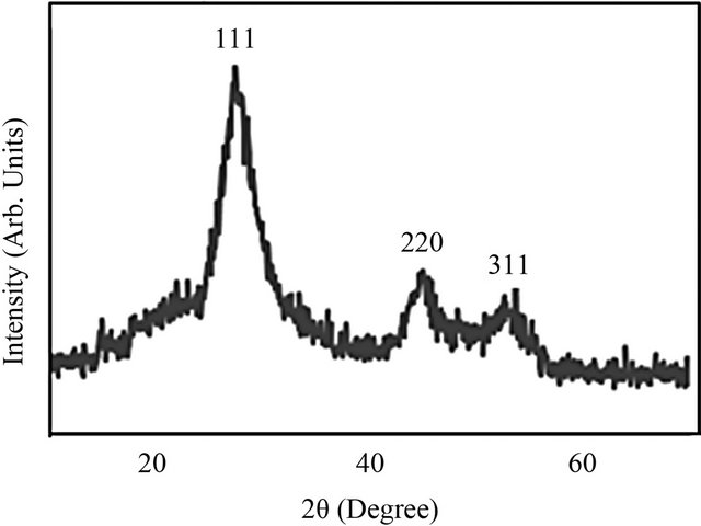
Figure 1. XRD patterns of CdS/PVA nanocomposites (15 cycles).
Electric properties of the obtained samples were measured by immittance measurer E7-20 in frequency range from 200 Hz to 1 MHz. The samples of CdS/PVA were arranged between the metallic electrodes of sandwich geometry. The measured CdS/PVA nanocomposites films were 70 µm, 340 µm and 195 µm in thickness for the samples of 3, 7 and 10 formation cycles. The thickness of PVA made 80 µm. Voltage feeded the sample reached 1 V.
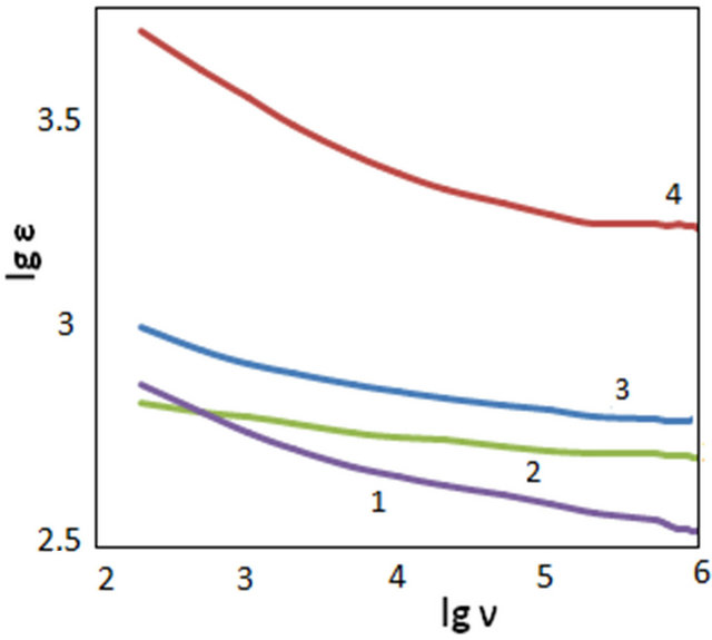
There has been considered frequency dependence of dielectric permittivity for the different samples. The investigated samples differed from each other by number of conducted cycles. Figure 2 shows the results of measurements of frequency dependence on temperatures (30˚C and 80˚C). As can be seen from Figure 2, at increasing cycles number dielectric permittivity (ε) of nanocomposites increases relative to PVA. At the initial stages (Figure2 at 3 cycles) with increase of cycles number permittivity of samples increases. At the same time at increasing cycles number (from 7 to 10) permittivity decreases. Decrease of dielectric permittivity, when cycles increase in number, is, probably connected with change in concentration of nanoparticles in a PVA film volume. Comparison of Figures 2(a) and (b) displays that at the increase of temperature, dielectric permittivity of nanocomposites increases. Change of permittivity from temperature depends on frequency. As can be seen from the Figure under 3 growth cycles permittivity of the samples is higher than PVA film. Exception is frequency field less than 500 Hz. With increase in cycle number till 7 permittivity increases. Further increasing cycle number (10 cycles) leads to decrease of permittivity of samples.
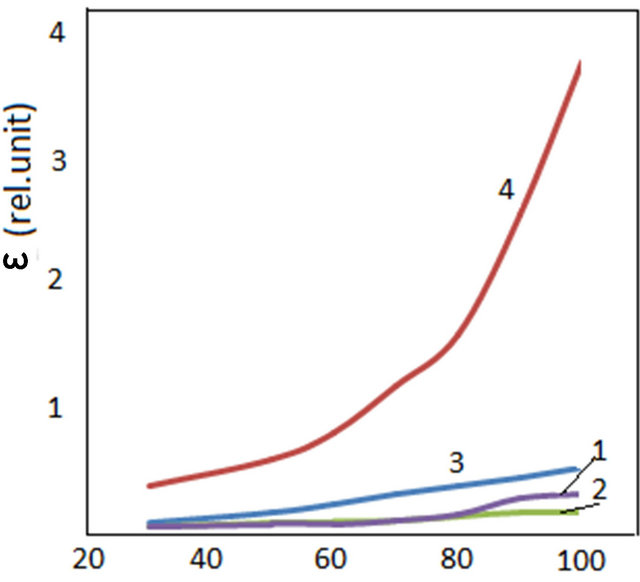
Figure 3 shows temperature dependence of permittivity at frequency of 500 Hz and 50 kHz. As can be seen from the figure changing frequency leads to alternating the character of change of permittivity depending on frequency.
At greater frequencies (in the frequency range of 10 - 1000 kHz) there is very weak change of dielectric permittivity (Figure 2). Starting from frequency range of 10 kHz at decreasing frequencies permittivity of the samples increase. This process actively proceeds at increasing temperature. With increase in temperature at lowering frequencies permittivity increases. As a rule with increase in temperature permittivity increases. It is, probably, related to thermal activation of polarization factors with increasing temperature. Because with increase in temperature bond of domains with matrix weakens and dipoles orient themselves somewhat easily in external field. Increase in value of permittivity at relatively greater frequencies is connected with change in the character of polarization of polymer nanocomposites.
As already mentioned above, anomalistic behavior of
 (a)
(a) (b)
(b)
Figure 2. Frequency dependence of permittivity of CdS/PVA nanocomposites; (a) T = 30˚C; (b) T = 80˚C: 1—PVA; 2—CdS/PVA 3c; 3—CdS/PVA 10c; 4—CdS/PVA 7c.
dielectric permittivity change depending on number of growth cycles is, probably, associated with redistribution of nanoparticles in a volume of polyvinyl alcohol film. In Figure 4 there is shown dependence of change of films mass on cycles number. As can be seen from the figure, at the start of growth this dependence is of sharp character. At the initial stages of growth nanoparticles of cadmium sulfide are formed in a volume of polymer matrix itself. In this case there is even (1 - 2 cycles of the formation) distribution of nanoparticles in volume. At increasing cycles number the adsorption centers in a polymer matrix volume are filled and the growth in a volume ceases [23,24].
As a result the process of growth mainly takes place on a sample surface. In addition, as a result of interaction of charged (or polar) nanoparticles and double electric layer, which is formed between polymer thin films and electrolyte solution, Nanoparticles of semiconductor migrate from a polymer matrix volume to near surface field. As a result of this process, with increasing cycle number
 (a)
(a) (b)
(b)
Figure 3. Temperature dependence of dielectric permittivity of CdS/PVA nanocomposites; (a) ν = 500 Hz; (b) ν = 50 kHz: 1—PVA; 2—CdS/PVA 3c; 3—CdS/PVA 10c; 4—CdS/PVA 7c.
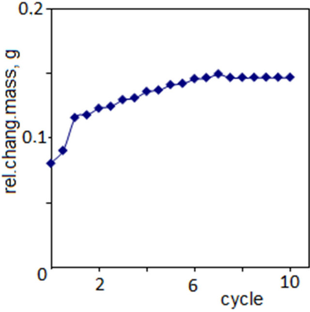
Figure 4. Dependence of the film mass versus the number of cycles of formation.
dielectric permittivity of the samples decreases. As it has been shown in our earlier works [25] it results in rise of surface resistivity of the samples. When cycles number grows the cross-section resistance of the samples decreases. This is connected with decreasing number of semiconductor particles in the volume. Figure 5 demon-

Figure 5. Gross-section of a CdS/PVA film nanocomposite of 15 cycles (film is 350 µm in thickness).
strates a photo of the cross-section of CdS/PVA films for 15 growth cycles. As can be seen from the Figure, there is heterogeneous distribution of particles over the volume.
Nanoparticles of cadmium sulfide in these nanocompsites are mainly formed in near surface field. It is, probably, connected with the following factors; at the initial stage of growth in a polymer matrix volume the sorption centers are completely filled. Then the growth chiefly takes place in near surface field. In addition, as a result of interaction of nanoparticles, having been formed in a polymer matrix volume, and electrolyte solution nanoparticles migrate to near surface field.
5. Conclusion
Thus, CdS/PVA composites were obtained from electrolyte solutions on the base of SILAR technique from ethylene glycol solutions. Investigations of frequency dependence of the samples showed that dielectric permittivity of samples depended on temperatures and growth cycles. The character of distribution of nanoparticles depend on cycles number. Change in cycles number leads to changing the character of nanoparticles distribution. These factors also influence on values of dielectric permittivity of CdS/PVA nanocomposites.
6. Acknowledgements
This work was supported by EC in the framework of FP7 NAPEP project, Grant Agreement #2666000.
REFERENCES
- T.-P. Nguyen, “Polymer-Based Nanocomposites for Organic Optoelectronic Devices. A Review,” Surface and Coatings Technology, Vol. 206, No. 4, 2001, pp. 742-752. doi:10.1016/j.surfcoat.2011.07.010
- M. B. Muradov, “The Influence of the Type of Polymer Matrix on the Photoluminescence from Cadmium Sulfide Nanoparticles,” Optoelectronics and Advanced Materials—Rapid Communications, Vol. 2, No. 2, 2008, p. 85.
- Rajesh, T. Ahuja and D. Kumar, “Recent Progress in the Development of Nano-Structured Conducting Polymers/ Nanocomposites for Sensor Applications,” Sensors and Actuators B: Chemical, Vol. 136, No. 1, 2009, pp. 275- 286. doi:10.1016/j.snb.2008.09.014
- M. B. Muradov, “Proceedings of 2nd International Conference on Lasers and Their Application,” Tehran, 1993.
- N. V. Hullavarad and S. S. Hullavarad, “Synthesis and Characterization of Monodispersed CdS Nanoparticles in SiO2 Fibers by Sol Gel Method,” Photonics and Nanostructures—Fundamentals and Applications, Vol. 5, No. 15, 2007, p. 156.
- K. J. Mispa, P. Subramaniam and R. Murugesan, “Microwave-Assisted Route for Synthesis of Nanosized Metal Sulphides,” Chalcogenide Letter, Vol. 7, No. 5, 2010, p. 335.
- N. Ghows and M. H. Entezari, “A Novel Method for the Synthesis of CdS Nanoparticles without Surfactant,” Ultrasonics Sonochemistry, Vol. 18, No. 1, 2011, pp. 269- 275. doi:10.1016/j.ultsonch.2010.06.008
- R. S. Yadav, P. Mishra, R. Mishra, M. Kumar and A. C. Pandey, “Growth Mechanism and Optical Property of CdS Nanoparticles Synthesized Using Amino-Acid Histidine as Chelating Agent under Sonochemical Process,” Ultrasonics Sonochemistry, Vol. 17, No. 1, 2010, pp. 116-122. doi:10.1016/j.ultsonch.2009.04.011
- M. Kristl, I. Ban, A. Danč, V. Danč and M. Drofenik, “A Sonochemical Method for the Preparation of Cadmium Sulfide and Cadmium Selenide Nanoparticles in Aqueous Solutions,” Ultrasonics Sonochemistry, Vol. 17, No. 5, 2010, pp. 916-922. doi:10.1016/j.ultsonch.2009.12.013
- S. Chen, M. Paulose, C. Ruan, G. K. Mor, O. K. Varghese, D. Kouzoudis and C. A. Grimes, “Electrochemically Synthesized CdS Nanoparticle-Modified TiO2 Nanotube-Array Photoelectrodes: Preparation, Characterization, and Application to Photoelectrochemical Cells,” Journal of Photochemistry and Photobiology A: Chemistry, Vol. 177, No. 2-3, 2006, pp. 177-184. doi:10.1016/j.jphotochem.2005.05.023
- J. Y. Lee, Y. S. Kang and Y. J. Kim, “A Study on a New Synthetic Method of CdS and CdSe Nanoparticles and Their Organic/Inorganic Nanocomposite,” International Journal of Nanoscience, Vol. 1, No. 5, 2002, p. 501. doi:10.1142/S0219581X02000577
- H. N. Cui, M. F. Costa, V. Teixeira and J. Zhang, “Solution-Grown Method of CdS Film by Ultrasonical Colloid Chemistry Deposition Technique,” International Journal of Photoenergy, Vol. 2006, 2006, Article ID: 24916. doi:10.1155/IJP/2006/24916
- M. Karimi, M. Rabiee, F. Moztarzadeh, M. Tahriri and M. Bodagh, “RETRACTED: Controlled Synthesis, Characterization and Optical Properties of CdS Nanocrystalline Thin Films via Chemical Bath Deposition (CBD) Route,” Current Applied Physics, Vol. 9, No. 6, 2009, pp. 1263- 1268. doi:10.1016/j.cap.2009.02.006
- C. D. Lokhande, B. R. Sankapa, H. M. Pathan, M. Muller, M. Giersig and H. Tributsch, “Some Structural Studies on Successive Ionic Layer Adsorption and Reaction (SILAR)-Deposited CdS Thin Films,” Applied Surface Science, Vol. 181, No. 3-4, 2001, pp. 277-282. doi:10.1016/S0169-4332(01)00392-0
- S. K. Panda, S. Chakrabarti, B. Satpati, P. V. Satyam and S. Chaudhuri, “Optical and Microstructural Characterization of CdS-ZnO Nanocomposite Thin Films Prepared by Sol-Gel Technique,” Journal of Physics D: Applied Physics, Vol. 37, No. 4, 2004, p. 628. doi:10.1088/0022-3727/37/4/014
- F. Nicolau and J. C. Menard, “Solution Growth of ZnS, CdS and Zn1−xCdxS Thin Films by the Successive Ionic-Layer Adsorption and Reaction Process; Growth Mechanism,” Journal of Crystal Growth, Vol. 92, No. 1-2, 1988, pp. 128-142. doi:10.1016/0022-0248(88)90443-5
- V. V. Klechkovskaya, V. N. Maslov, M. B. Muradov and S. А. Semiletov, “Research Process of Growth and Structure of Semiconductors thin Films CdS and ZnS and Alloy on Their Basis Received on the Mechanism Ion-Layered Chemosorbsion from Solutions of Electrolytes,” Kristallografiya, Vol. 34, No. 1, 1989, p. 182.
- S. Lindroos, T. Kanniainen and R. E. Leskela, “Deposition of Manganese-Doped Zinc Sulfide Thin Films by the Successive Ionic Layer Adsorption and Reaction (SILAR) Method,” Thin Solid Films, Vol. 263, No. 1, 1995, pp. 79-84. doi:10.1016/0040-6090(95)06558-X
- A. Agasiyev and M. B. Muradov, “Formation of Nanoparticles CdS in Volume of a Polymeric Matrix,” Pisma v Zurnal Technicheskoy Fiziki, Vol. 17, No. 13, 1991, p. 54.
- V. P. Tolstoy, “Successive Ionic Layer Deposition. The Use in Nanotechnology,” Russian Chemical Reviews, Vol. 75, No. 2, 2006, p. 161. doi:10.1070/RC2006v075n02ABEH001197
- А. V. Volkov, M. A. Moskvina, I. V. Karachevtsev, O. V. Lebedeva, А. L. Volynski and V. Bakeev, “The Structure and Conductivity of the Highly Dispersed CuS Polymer Compositions Obtained IN-SITUA,” Polymer Science, Series A. Polymer Physics Vysokomolekulyarnye Soedineniya, Vol. 40, No. 6, 1998, p. 976.
- N. A. Shah, R. R. Sagar, W. Mahmood and W. A. A. Syed, “Cu-Doping Effects on the Physical Properties of Cadmium Sulfide Thin Films,” Journal of Alloys and Compounds, Vol. 512, No. 1, 2012, pp. 185-189. doi:10.1016/j.jallcom.2011.09.060
- M. B. Muradov, A. Sh. Abdinov, R. H. Hacimamedov and G. M. Eyvazova, “Dielectric Properties of Nanocomposites on the Basis of Copper Sulfide Nanoparticles and a Polymer Matrix,” Surface Engineering and Applied Electrochemistry, Vol. 45, No. 2, 2009, pp. 167-170. doi:10.3103/S1068375509020161
- M. B. Muradov, G. M. Eyvazova and A. N. Bagirov, “The Effect of Solutions Concentrations on the Optical Properties of CdS Nanoparticles Formed in the Polymeric Matrix,” Journal of Optoelectronics and Advanced Materials, Vol. 9, No. 5, 2007, p. 1411.
- M. B. Muradov, M. A. Nuriev and G. M. Eyvazova, “Conductivity of Composites on Base of Polymer Matrix and of Nanoparticles Copper Sulfide,” Transactions ANAS, Vol. 27, No. 2, 2007, p. 125.
NOTES
*This work was supported by EC in the framework of FP7 NAPEP project, Grant Agreement #2666000.
#Corresponding author.