90 R. K. VISHWAKARMA ET AL.
30
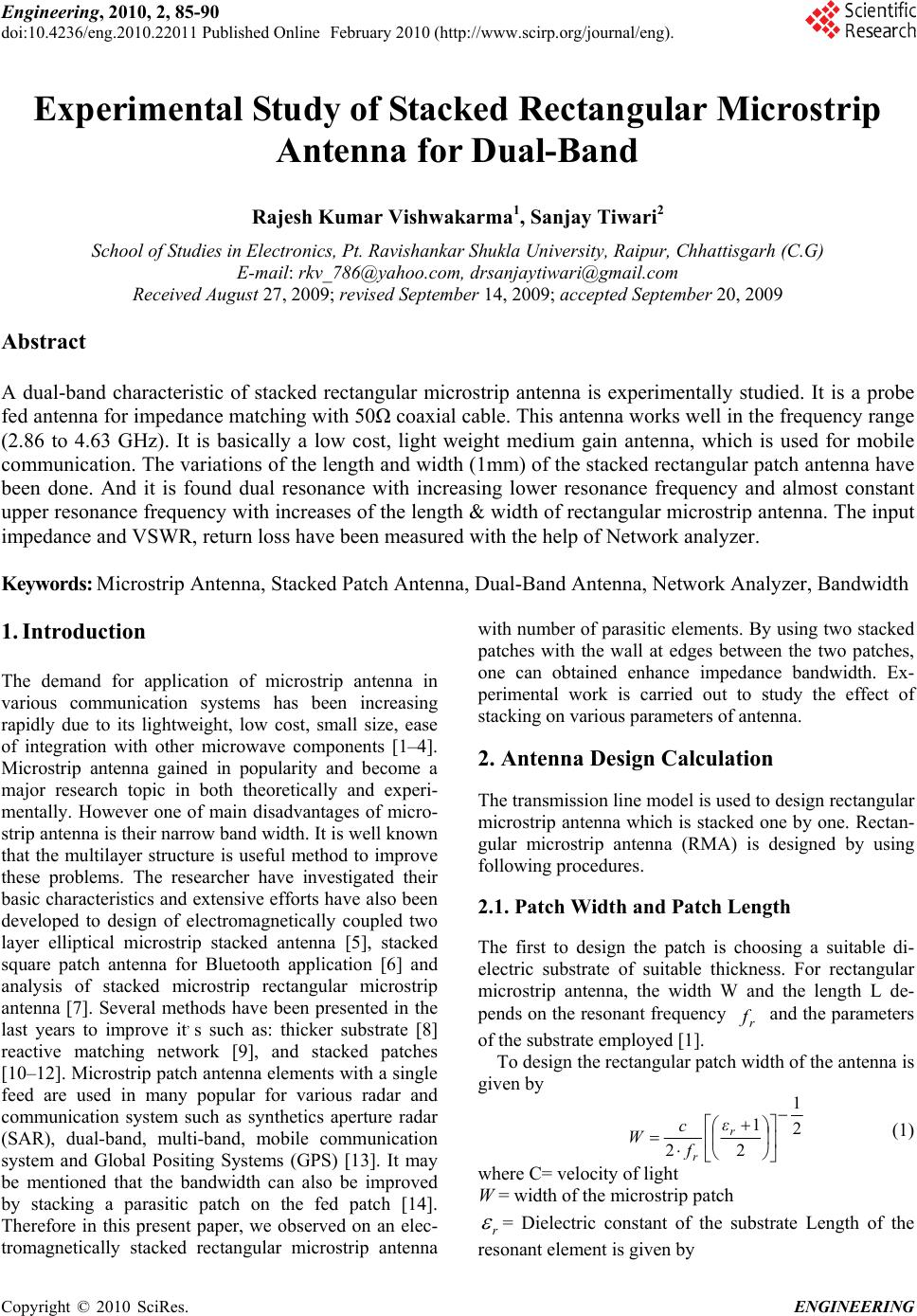
40
50
60
70
80
90
2345
Dimension of patches (mm)
Real part of input impedance (ohm
)
6
R_part (f
1
)
R_part (f
2
)
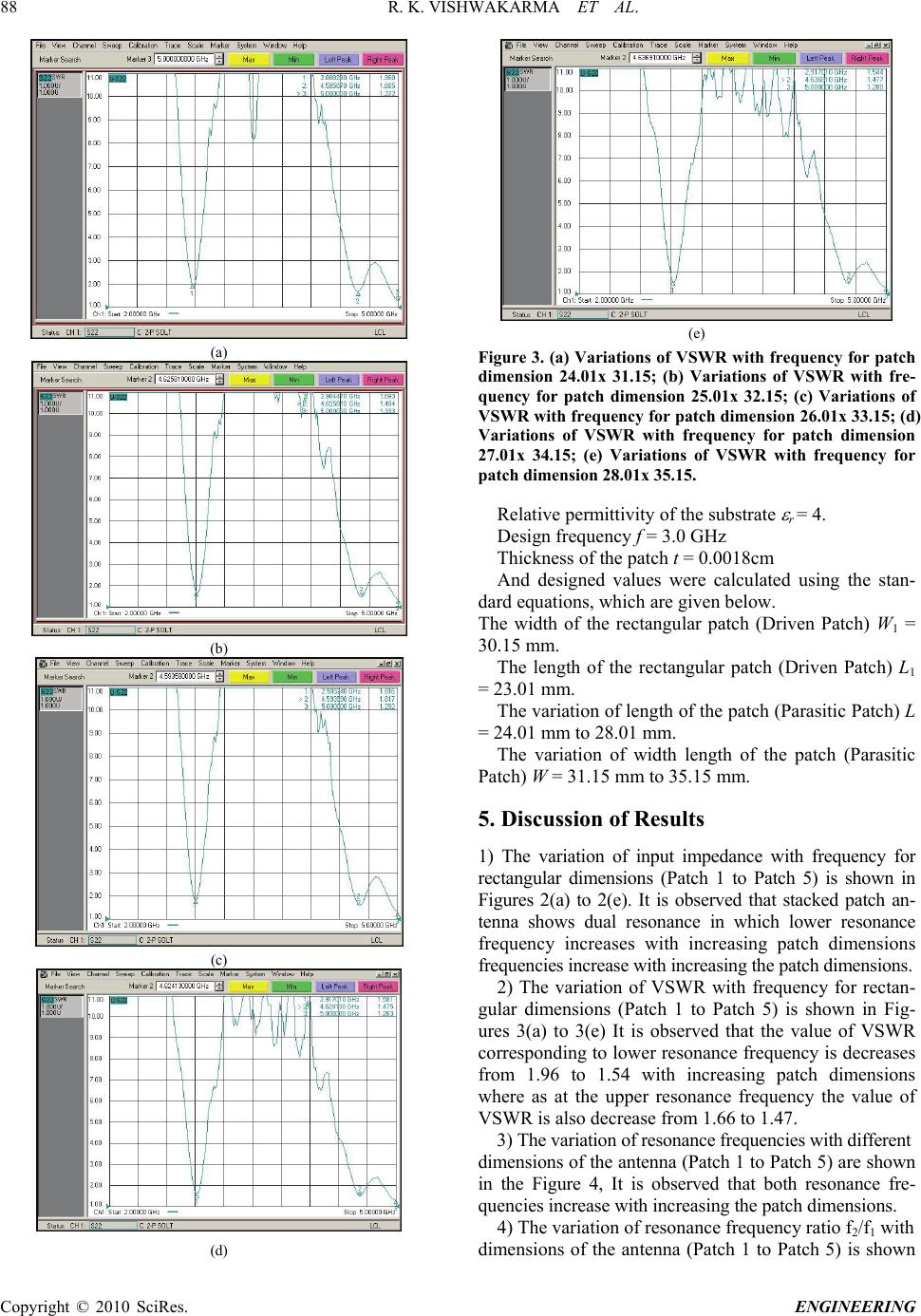
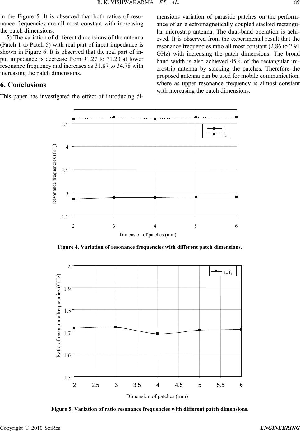
Figure 6. Variations of patch dimensions with real part of input impedance.
7. Acknowledgments
The authors would like to thank Professors Arun Kumar
and Shri R. K. Malaviya of the Space Application Centre,
Indian Space Research Organization Ahmedabad, for
providing the measurement facilities.
8. References
[1] J. l. BahI, and P. Bhartia, Microstrip Antennas, Dedham,
MA, (USA) Artech House, 1980.
[2] J. R. James, P. S. Hall, and C. Wood, “Microstrip antenna
theory and design” IEE Electromagnetic Wave, Series 12
London, U. K. Peter Peregrinus, 1981.
[3] K. C. Gupta, “Recent advance in microstrip antenna,”
Microwave Journal, No. 27, pp. 50–67, 1984.
[4] S. A. Long and M. D. Walton, “A dual-frequency circu-
lar-disc antenna,” IEEE Transactions on Antenna and
Propagation USA, AP-27, pp. 270–273, 1979.
[5] R. L. Yadava and B. R. Vishvakarma, “Analysis of elec-
tromagnetically coupled two-layer elliptical microstrip
stacked antennas,” International Journal of Electronics,
Vol. 87, No. 8, pp. 981–993, 2000.
[6] A. B. Nandgaonkar and S. B. Deosarkar, “Broadband
stacked patch antenna for bluetooth applications,” Journal
of Microwaves, Optoelectronics and Electromagnetic
Application, Vol. 8, No. 1, pp. 1–5, 2009.
[7] I. K. Moussa and D. A. E. Mohamed and I. badran,
“Analysis of stacked rectangular microstrip antenna,” 24th
National Radio Science Conference, March 13-15, pp. 1–
10, 2007.
[8] W. Chen, K. F. Lee, and R. O. Lee, “Input impedance of
coaxially fed rectangular microstrip antenna on electri-
cally thick substrate,” Microwave optical Technology
Letters, Vol. 6, No. 6, pp. 387–390, 1993.
[9] F. Pues and R. Van De Capelle, “An impedance matching
technique for increasing the bandwidth of microstrip an-
tenna,” IEEE Transactions on Antennas Propagation, Vol.
37, pp. 1345–1354, 1989.
[10] J. S. Dahel and K. F. Lee,“A dual-frequency stacked mi-
crostrip antenna,” IEEE AP-S International Symposium
Digest, pp. 308–30–11, 1982.
[11] K. F. Lee, K. Y. Ho, and J. S. Dahele, “Circular-disk mi-
crostrip antenna with air gap”, IEEE Transactions on An-
tenna (USA) and Propagation, AP-32, pp. 880–884, 1984.
[12] J. S. Dahele, K. F. Lee, and D. P. Wong, “Dual frequency
stacked annular ring microstrip antenna,” IEEE Transac-
tions Antennas and Propagation (USA) AP-35, pp. 1281–
1285, 1987.
[13] D. M. Pozar and S. M. Duffy. “A dual-band circular po-
larized aperture-coupled stacked microstrip antenna for
global positioning satellite, “IEEE Transactions on An-
tennas and Propagation (USA), Vol. 45, No. 11, pp.
1618–1625, 1997.
[14] S. Egashira and E. Nishiyama “Stacked microstrip an-
tenna with wide bandwidth and high gain,” IEEE Trans-
actions on Antennas and Propagation (USA) Vol. 44, No.
11, pp. 1533–1534, 1996.
[15] R. E. Harrington, “Time harmonic electromagnetic field,”
Ms Graw-Hill, New Delhi, 1979.
Copyright © 2010 SciRes. ENGINEERING