Paper Menu >>
Journal Menu >>
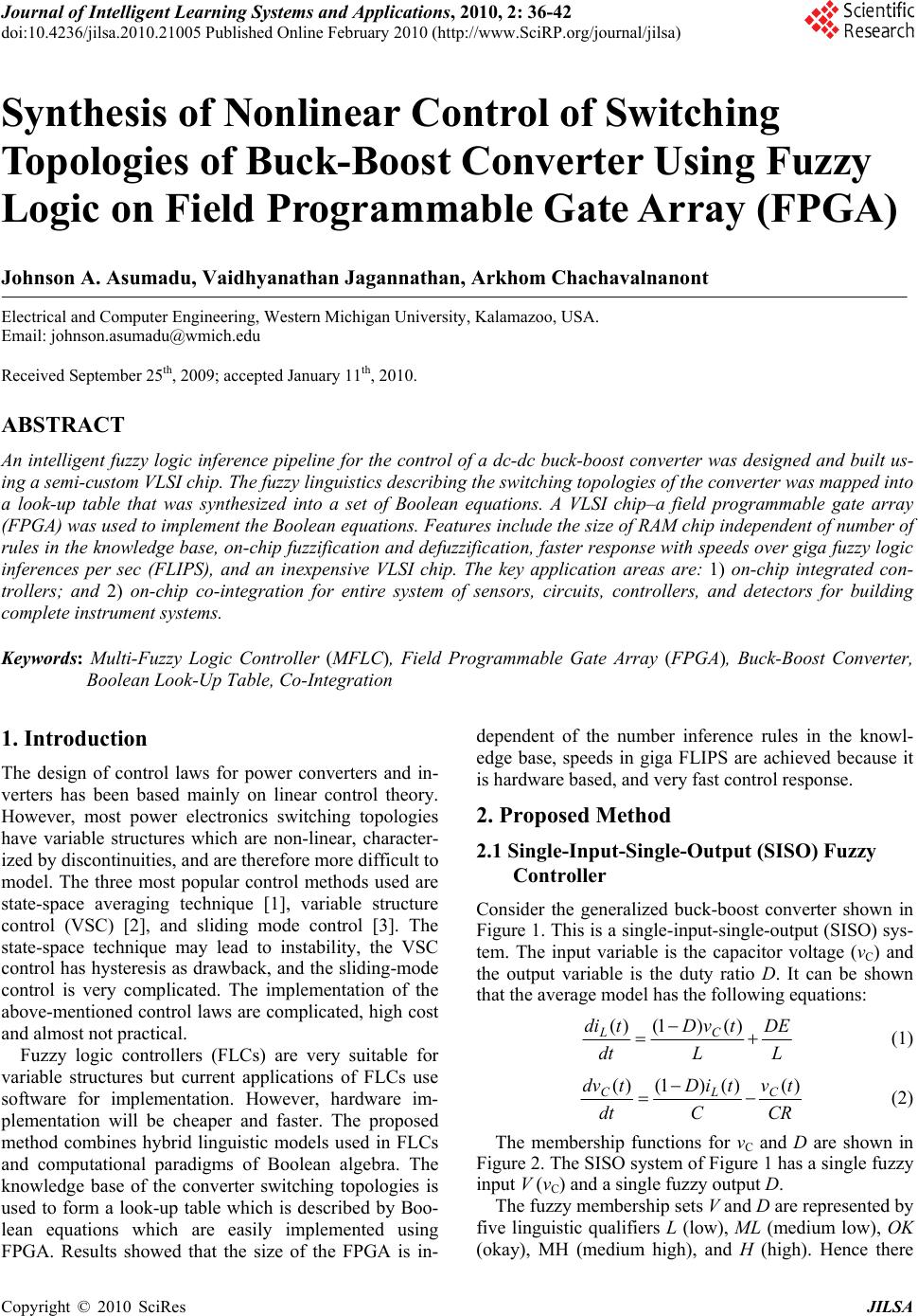 Journal of Intelligent Learning Systems and Applications, 2010, 2: 36-42 doi:10.4236/jilsa.2010.21005 Published Online February 2010 (http://www.SciRP.org/journal/jilsa) Copyright © 2010 SciRes JILSA Synthesis of Nonlinear Control of Switching Topologies of Buck-Boost Converter Using Fuzzy Logic on Field Programmable Gate Array (FPGA) Johnson A. Asumadu, Vaidhyanathan Jagannathan, Arkhom Chachavalnanont Electrical and Computer Engineering, Western Michigan University, Kalamazoo, USA. Email: johnson.asumadu@wmich.edu Received September 25th, 2009; accepted January 11th, 2010. ABSTRACT An intelligent fuzzy logic inference pipeline for the control of a dc-dc buck-boost converter was designed and built us- ing a semi-custom VLSI chip. The fuzzy linguistics describing the switching topologies of the converter was mapped into a look-up table that was synthesized into a set of Boolean equations. A VLSI chip–a field programmable gate array (FPGA) was used to implement the Boolean equations. Features include the size of RAM chip independent of number of rules in the knowledge base, on-chip fuzzification and defuzzification, faster response with speeds over giga fuzzy logic inferences per sec (FLIPS), and an inexpensive VLSI chip. The key application areas are: 1) on-chip integrated con- trollers; and 2) on-chip co-integration for entire system of sensors, circuits, controllers, and detectors for building complete instrument systems. Keywords: Multi-Fuzzy Logic Controller (MFLC), Field Programmable Gate Array (FPGA), Buck-Boost Converter, Boolean Look-Up Table, Co-Integration 1. Introduction The design of control laws for power converters and in- verters has been based mainly on linear control theory. However, most power electronics switching topologies have variable structures which are non-linear, character- ized by discontinuities, and are therefore more difficult to model. The three most popular control methods used are state-space averaging technique [1], variable structure control (VSC) [2], and sliding mode control [3]. The state-space technique may lead to instability, the VSC control has hysteresis as drawback, and the sliding-mode control is very complicated. The implementation of the above-mentioned control laws are complicated, high cost and almost not practical. Fuzzy logic controllers (FLCs) are very suitable for variable structures but current applications of FLCs use software for implementation. However, hardware im- plementation will be cheaper and faster. The proposed method combines hybrid linguistic models used in FLCs and computational paradigms of Boolean algebra. The knowledge base of the converter switching topologies is used to form a look-up table which is described by Boo- lean equations which are easily implemented using FPGA. Results showed that the size of the FPGA is in- dependent of the number inference rules in the knowl- edge base, speeds in giga FLIPS are achieved because it is hardware based, and very fast control response. 2. Proposed Method 2.1 Single-Input-Single-Output (SISO) Fuzzy Controller Consider the generalized buck-boost converter shown in Figure 1. This is a single-input-single-output (SISO) sys- tem. The input variable is the capacitor voltage (vC) and the output variable is the duty ratio D. It can be shown that the average model has the following equations: L DE L tvD dt tdi C L )()1( )( (1) CR tv C tiD dt tdv C L C)( )()1( )( (2) The membership functions for vC and D are shown in Figure 2. The SISO system of Figure 1 has a single fuzzy input V (vC) and a single fuzzy output D. The fuzzy membership sets V and D are represented by five linguistic qualifiers L (low), ML (medium low), OK (okay), MH (medium high), and H (high). Hence there 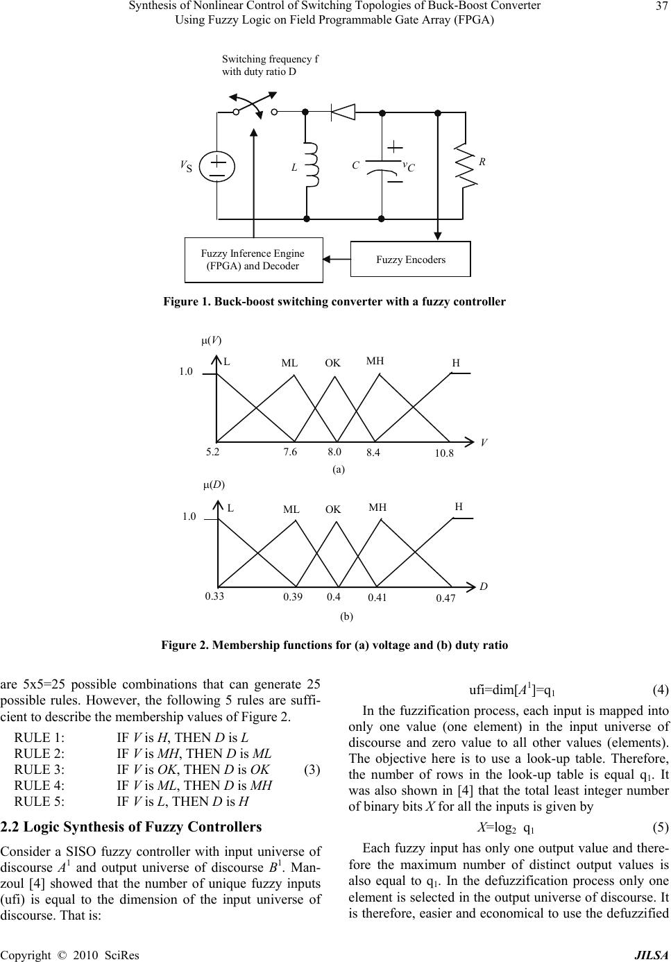 Synthesis of Nonlinear Control of Switching Topologies of Buck-Boost Converter Using Fuzzy Logic on Field Programmable Gate Array (FPGA) 37 L C R vC Fuzzy Encoders Fuzzy Inference Engine (FPGA) and Decoder VS Switching frequency f with duty ratio D Figure 1. Buck-boost switching converter with a fuzzy controller (b) L (D) OKML 0.39 0.40.41 H MH 1.0 0.47 0.33 D L (V) OKML 7.68.0 8.4 H MH 1.0 10.8 5.2 V (a) Figure 2. Membership functions for (a) voltage and (b) duty ratio are 5x5=25 possible combinations that can generate 25 possible rules. However, the following 5 rules are suffi- cient to describe the membership values of Figure 2. RULE 1: IF V is H, THEN D is L RULE 2: IF V is MH, THEN D is ML RULE 3: IF V is OK, THEN D is OK (3) RULE 4: IF V is ML, THEN D is MH RULE 5: IF V is L, THEN D is H 2.2 Logic Synthesis of Fuzzy Controllers Consider a SISO fuzzy controller with input universe of discourse A1 and output universe of discourse B1. Man- zoul [4] showed that the number of unique fuzzy inputs (ufi) is equal to the dimension of the input universe of discourse. That is: ufi=dim[A1]=q1 (4) In the fuzzification on (5) Each fuzzy input ha fo process, each input is mapped into ly one value (one element) in the input universe of discourse and zero value to all other values (elements). The objective here is to use a look-up table. Therefore, the number of rows in the look-up table is equal q1. It was also shown in [4] that the total least integer number of binary bits X for all the inputs is given by X=log2 q 1 s only one output value and there- re the maximum number of distinct output values is also equal to q1. In the defuzzification process only one element is selected in the output universe of discourse. It is therefore, easier and economical to use the defuzzified Copyright © 2010 SciRes JILSA  Synthesis of Nonlinear Control of Switching Topologies of Buck-Boost Converter Using Fuzzy Logic on Field Programmable Gate Array (FPGA) 38 outputs in the look-up table. If the there are p elements (p <q1) in the output universe of discourse, the dimension of the output universe of discourse is given as dim[B1]=p (6) The total least intege th Y=log2 p (7) 3. Buck-Boost Con er to control the output voltage im[V]=dim[D]=29 (8) From (5) the least th 29=5 Table 1. Summary of the controller computations Input Voltage Fuzzified Input Output Duty Ratio (X) r number of binary bits Y for all e outputs is given by verter Fuzzy Controller 3.1 Fuzzy Controller Consider a SISO controll of the buck-boost converter of Figure 1. The input vari- able is the voltage and output variable is the duty ratio. The duty ratio maintains the voltage at a selected value. The ranges of capacitor voltage (vC) and duty ratio D are (5.2 to 10.8) V and (0.33 to 0.47) respectively. The membership values are in the interval [0, 1], where 0 denotes no membership and 1 denotes full membership. Assume that 1 1 number of binary bits to represent e input values is given as X=log2 Similarly, using (6) the least number of binary bits to represent output values is given as Y=log2 29=5 In Appendix I the 5 rules of (3) are expressed numeri- cally. The fuzzy relation obtained is too big to be shown here because of the size (29x29 matrix). Table 1 of Ap- pendix I shows the summary of the complete computa- tions of the controller. 3.2 Look-Up Table The look-up table representing the fuzzy controller is given in Table 2. The input universe of discourse has dimension of 29 and the output universe has dimension of 29. The look-up can be described by 7-variable Boo- lean equations. That is, f 0= (5,6,8,9,10,12,16,17,1923,26,27,28) f 1= (2,4,5,7,8,10,11,14,17,18,21,24,27) f 2= (2,3,5,6,8,9,14,15,16,21,22,24, 25,27,28,29) f 3= (1,5,6,7,14,16,17,18,19,20,24,25,26) (9) f 4= (1,2,3,4,14,24,25,26,27,28,29) f 5= (1,2,3,4,5,6,7,8,9,10,11,12,13,16,17,18,19, 20, 21, 22, 23) f6= (1,2,3,4,5,6,7,8,9,10,11,12,13,14,15) Fuzzy Output 0.0 - 5.20 1.0,.0 *0,0,.08,.16,.25,6,.75,.83,.91,1.0 0.0, 0.0, ., ., ., 0.33,.41,.5,.58,.6120 5.21 - 5.40 0.0, 1.0, 0.0, ., ., ., 0.0 *, *, . .7 .08,.08,.08,.16,.25,.33,.41,.5,.58,.66,.75,.83,.91,.91118 5.41 - 5.60 0.0, ., ., 1.0, ., ., ., 0.0 *,.16,.16,.16,.16,.25,.33,.41,.5,.58,.66,.75,.83,.83,.83 116 5.61 - 5.80 0.0, ., ., 1.0, ., ., ., 0.0 *,.25,.25, ,.25, ,.25, ,.25,.33,.41,.58,.66,.75,.75,.75,.75 114 5.81 - 6.00 0.0, ., ., 1.0, ., ., ., 0.0 *,.33,.33,.33,.33,.33,.33,.41,.5,.58,.66,.66,.66,.66,.66 111 6.01 - 6.20 0.0, ., ., 1.0, ., ., ., 0.0 *,.41,.41,.41,.41,.41,.41,.41,.5,.58,.58,.58,.58,.58,.58 109 6.21 - 6.40 0.0, ., ., 1.0, ., ., ., 0.0 *,.5,.5,.5,.5,.5,.5,.5,.5,.5,.5,.5,.5,.5,.5 .5,.58,. ,.41,.41 106 6.41 - 6.60 0.0, ., ., 1.0, ., ., ., 0.0 58,.58,.58,.58,.58,.5,.41,.41,.41,.41,.41103 6.61 - 6.80 0.0, ., ., 1.0, ., ., ., 0.0 *,.5,.66,.66,.66,.66,.66,.58,.5,.41,.33,.33,.33,.33,.33 *,5 101 6.81 - 7.00 0.0, ., ., 1.0, ., ., ., 0.0 .5,.75,.75,.75,.75,.66,.58,.5,.41,.33,.25, ,.25, ,.25, ,.299 7.01 - 7.20 0.0, ., ., 1.0, ., ., ., 0.0 *,.5,.83,.83,.83,.75,.66,.58,.5,.41,.33,.25,.16,.16,.16 98 7.21 - 7.40 0.0, ., ., 1.0, ., ., ., 0.0 *,.5,.91,.91,.83,.75,.66,.58,.5,.41,.33,.25,.16,.08,.08 97 7.41 - 7.60 0.0, ., ., 1.0, ., ., ., 0.0 *,.5,1.0,.91,.83,.75,.66,.58,.5,.41,.33,.25,.16,.08,.0 96 7.61 - 7.80 0.0, ., ., 1.0, ., ., ., 0.0 **,.5,.5,.5,.5,.5,.5,.5,.5,.5,.5,.41,.33,.25,.16,.08,0.0 94 7.81 - 8.00 0.0, ., ., 1.0, ., ., ., 0.0 **,.5,1.0,.5,** 0,.08,.16,.25,.33,.4,.5,.5,.5,.5,.5,** 70 8.01 - 8.20 0.0, ., ., 1.0, ., ., ., 0.0 1,.5,.5,.5,.5,.545 8.21 - 8.40 0.0, ., ., 1.0, ., ., ., 0.0 0,.08,.16,.25,.33,.41,.5,.58,.66,.75,.83,.91,1.0,.5,* 43 8.41 - 8.60 0.0, ., ., 1.0, ., ., ., 0.0 .08,.08,.16,.25,.33,.41,.5,.58,.66,.75,.83,.91,.91,.5,* 42 8.61 - 8.80 0.0, ., ., 1.0, ., ., ., 0.0 .16,.16,.16,.25,.33,.41,.58,.66,.75,.75,.75,.75,.5,* .2* 41 8.81 - 9.00 0.0, ., ., 1.0, ., ., ., 0.0 5, ,.25, ,.25, ,.25,.33,.41,.58,.66,.75,.75,.75,.75,.5,40 9.01 - 9.20 0.0, ., ., 1.0, ., ., ., 0.0 .33,.33,.33,.33,.33,.41,.5,.58,.66,.66,.66,.66,.66,.5,* 38 9.21 - 9.40 0.0, ., ., 1.0, ., ., ., 0.0 .41,.41,.41,.41,.41,.41,.5,.58,.58,.58,.58,.58,.58,.5,* 36 9.41 - 9.60 0.0, ., ., 1.0, ., ., ., 0.0 .5,.5,.5,.5,.5,.5,.5,.5,.5,.5,.5,.5,.5,.5,* 58,.58,1,.41,* 33 9.61 - 9.80 0.0, ., ., 1.0, ., ., ., 0.0 .58,.58,.58,.58,.5,.41,.41,.41,.41,.41,.430 9.81 - 10.00 0.0, ., ., 1.0, ., ., ., 0.0 .66,.66,.66,.66,.66,.58,.5,.41,.33,.33,.33,.33,.33,.33,* 28 10.01 - 10.20 0.0, ., ., 1.0, ., ., ., 0.0 5,.75,.75,.75,.66,.58,.5,.41,.33,.25, ,.25, ,.25, ,.25,.25,* 25 10.21 - 10.40 0.0, ., ., 1.0, 0.0, 0.0 .83,.83,.83,.75,.66,.58,.5,.41,.33,.25,.16,.16,.16,.16,* 23 10.41 - 10.60 0.0, ., ., 0.0, 1.0, 0.0 .91,.91,.83,.75,.66,.58,.5,.41,.33,.25,.16,.08,.08,.08,* 21 10.61 - 10.8 0.0, ., ., 0.0, 0.0, 1.0 1.0,.91,.83,.75,.66,.58,.5,.41,.33,.25,.16,.08,.0,.0,* 20 NOTE: *=0,0,0 ** Duty ratio D=-0.0011051*X+0.4 ,0,0,0,0,0,0,0,0,0,0,0,0 =0,0,0,0,0,0,0,0,0,0,0,0,0 Copyright © 2010 SciRes JILSA 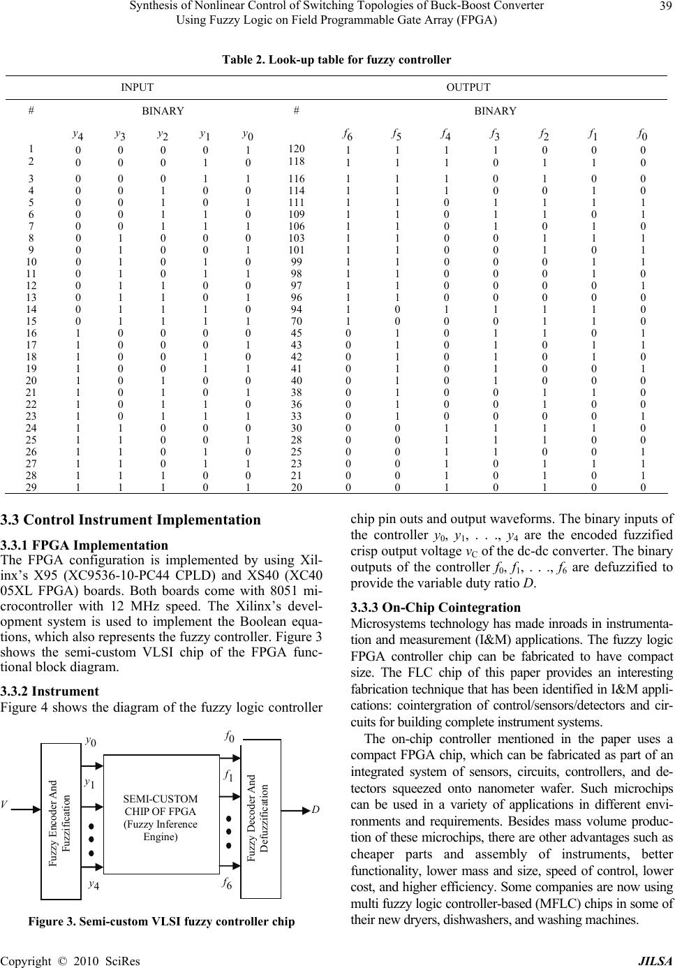 Synthesis of Nonlinear Control of Switching Topologies of Buck-Boost Converter Using Fuzzy Logic on Field Programmable Gate Array (FPGA) 39 y controller INPUT OUTPUT Table 2. Look-up table for fuzz BINARY RY BINA # y4 0 y3 0 y1 0 y0 1 # 120 118 f6 1 f5 1 f4 1 f2 0 f1 0 f0 0 1 2 0 0 y2 0 0 1 0 1 1 1 f3 1 0 1 1 0 3 0 0 0 1 1 11611101 0 0 4 0 0 1 0 0 11411100 1 0 5 0 0 1 0 1 11111011 1 1 6 0 0 1 1 0 10911011 0 1 7 0 0 1 1 1 10611010 1 0 8 0 1 0 0 0 10311001 1 1 9 0 1 0 0 1 10111001 0 1 10 0 1 0 1 0 9911000 1 1 11 0 1 01 1 9811000 1 0 12 0 1 1 0 0 9711000 0 1 13 0 1 1 0 1 9611000 0 0 14 0 1 1 1 0 9410111 1 0 15 0 1 1 1 1 7010001 1 0 16 1 0 0 0 0 4501011 0 1 17 1 0 0 0 1 4301010 1 1 18 1 0 0 1 0 4201010 1 0 19 1 0 0 1 1 4101010 0 1 20 1 0 1 0 0 4001010 0 0 21 1 0 1 0 1 3801001 1 0 22 1 0 1 1 0 3601001 0 0 23 1 0 1 1 1 3301000 0 1 24 1 1 0 0 0 3000111 1 0 25 1 1 0 0 1 2800111 0 0 26 1 1 0 1 0 2500110 0 1 27 1 1 0 1 1 2300101 1 1 28 1 1 1 0 0 2100101 0 1 29 1 1 1 0 1 2000101 0 0 3.3 ntrolstrument Iplemntat sing Xil- and XS40 (XC40 ram of the fuzzy logic controller Co Inmeion 3.3.1 FPGA Implementation The FPGA configuration is implemented by u inx’s X95 (XC9536-10-PC44 CPLD) 05XL FPGA) boards. Both boards come with 8051 mi- crocontroller with 12 MHz speed. The Xilinx’s devel- opment system is used to implement the Boolean equa- tions, which also represents the fuzzy controller. Figure 3 shows the semi-custom VLSI chip of the FPGA func- tional block diagram. 3.3.2 Instrument Figure 4 shows the diag f 0 SEMI-CUSTOM CHIP OF FPGA (Fuzzy Inference Engine) f1 Fuzzy Encoder And Fuzzification Fuzzy Decoder And Defuzzification f6 y4 y0 y1 D V Figure 3. Semi-custom VLSI fuzzy controller chip p pin outs anutput waveform The bry inpts of the controller y0, y1, . . ., y4 are the encoded fuzzified crisp output voltage vC of the dc-dc converter. The binary outputs of the controller f0, f1, . . ., f6 are defuzzified to provide the variable duty ratio D. 3.3.3 On-Chip Cointegration Microsystems technology has made inroads in instrumenta- tion and measurement (I&M) applications. The fuzzy logic FPGA controller chip can be fabricated to have compact size. The FLC chip of this paper provides an interesting fabrication technique that has been identified in I&M appli- cations: cointergration of control/sensors/detectors and cir- cuits for building complete instrument systems. s mass volume produc- e other advantages such as chi d os.inau Th a compact FPGA chip, which can be fabricated as part of an integrated system of sensors, circuits, controllers, and de- tectors squeezed onto nanometer wafer. Such microchips can be used in a variety of applications in different envi- ronments and requirements. Beside e on-chip controller mentioned in the paper uses tion of these microchips, there ar cheaper parts and assembly of instruments, better functionality, lower mass and size, speed of control, lower cost, and higher efficiency. Some companies are now using multi fuzzy logic controller-based (MFLC) chips in some of their new dryers, dishwashers, and washing machines. Copyright © 2010 SciRes JILSA 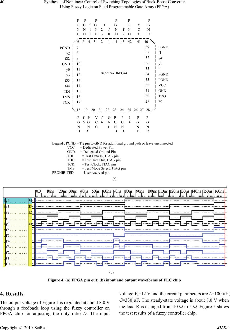 Synthesis of Nonlinear Control of Switching Topologies of Buck-Boost Converter Using Fuzzy Logic on Field Programmable Gate Array (FPGA) 40 Legend : PGND = Tie pin to GND for additional ground path or leave unconnected VCC = Dedicated Power Pin GND = Dedicated Ground Pin TDI = Test Data In, JTAG pin TDO = Test Data Out, JTAG pin TCK = Test Clock, JTAG pin TMS = Test Mode Select, JTAG pin PROHIBITED = User reserved pin (a) 6 5 4 3 2 1 43 42 41 40 44 7 8 9 10 11 12 13 14 15 16 17 18 19 20 2122 23 24 25 26 27 28 39 38 P P P G G P f G f G P P G V G N N 1 N 2 f f N C N D D 1 D 3 0 2 D C D N D 37 36 35 34 33 32 31 30 29 PGND y2 f22 GND y0 y3 f33 f44 TDI TMS TC K PGND f1 y4 y1 f3 PGND PGND VCC GND TDO F01 XC9536-10-PC44 P f P V f G P P f P P G 5 G C 6 N G G 4 G G N N C D N N N N D D D D D D (b) Figure 4. (a) FPGA pin out; (b) input and output waveforms of FLC chip 4. Results The output voltage of Figure 1 is regulated at about 8.0 V through a feedback loop using the fuzzy controller on FPGA chip for adjusting the duty ratio D. The input voltage Vs=12 V and the circuit parameters are L=100 H, C=330 F. The steady-state voltage is about 8.0 V when the load R is changed from 10 to 5 . Figure 5 shows the test results of a fuzzy controller chip. Copyright © 2010 SciRes JILSA 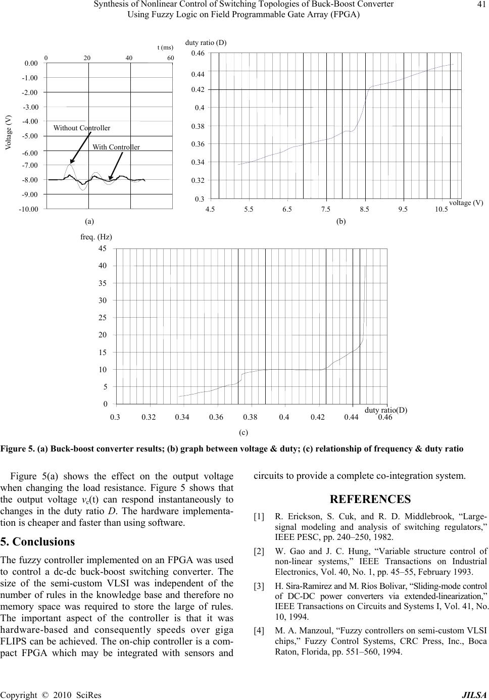 Synthesis of Nonlinear Control of Switching Topologies of Buck-Boost Converter Using Fuzzy Logic on Field Programmable Gate Array (FPGA) 41 -10.00 -9.00 -8.00 -7.00 -6.00 -5.00 -4.00 -3.00 -2.00 -1.00 0.00 020 40 60 t (ms) With Controlle r Without Controlle r Voltage (V) 0.3 0.32 0.34 0.36 0.38 0.4 0.42 0.44 0.46 4.55.56.57.58.59.5 10.5voltage (V) duty ratio (D) (a) (b) 0 5 10 15 20 25 30 35 40 45 0.30.320.34 0.360.380.40.420.440.46 duty ratio(D ) freq. (Hz) (c) Figure 5. (a) Buck-boost converter results; (b) graph between voltage & duty; (c) relationship of frequency & duty ratio Figure 5(a) shows the effect on the output voltage when changing the load resistance. Figure 5 shows that the output voltage vc(t) can respond instantaneously to changes in the duty ratio D. The hardware implementa- tion is cheaper and faster than using software. 5. Conclusions The fuzzy controller implemented on an FPGA was used to control a dc-dc buck-boost switching converter. The size of the semi-custom VLSI was independent of the number of rules in the k emory space was required to store the large of rules. t aspect of the controller is that it was ed and consequently speeds over giga circuits to provide a complete co-integration system. REFERENCES [1] R. Erickson, S. Cuk, and R. D. Middlebrook, “Large- signal modeling and analysis of switching regulators,” IEEE PESC, pp. 240–250, 1982. [2] W. Gao and J. C. Hung, “Variable structure control of non-linear systems,” IEEE Transactions on Industrial Electronics, Vol. 40, No. 1, pp. 45–55, February 1993. livar, “Sliding-mode contro via extended-linearization,” IEEE Transactions on Circuits and Systems I, Vol. 41, No. nowledge base and therefore no [3] H. Sira-Ramirez and M. Rios Bo of DC-DC power converters m The importan hardware-bas FLIPS can be achieved. The on-chip controller is a com- pact FPGA which may be integrated with sensors and l 10, 1994. [4] M. A. Manzoul, “Fuzzy controllers on semi-custom VLSI chips,” Fuzzy Control Systems, CRC Press, Inc., Boca Raton, Florida, pp. 551–560, 1994. Copyright © 2010 SciRes JILSA 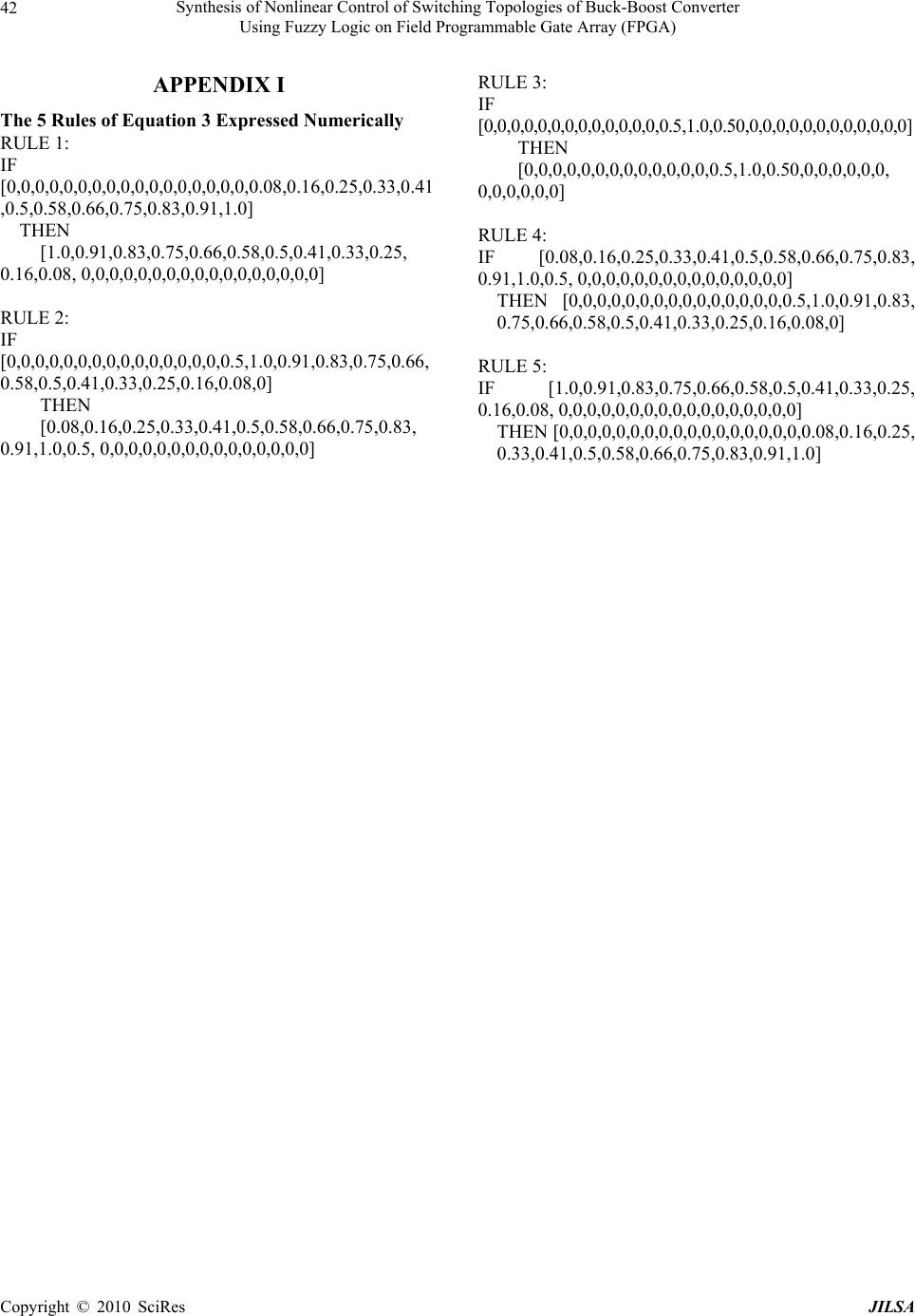 Synthesis of Nonlinear Control of Switching Topologies of Buck-Boost Converter 42 Using Fuzzy Logic on Field Programmable Gate Array (FPGA) APPENDIX I The 5 Rules of Equation 3 Expressed Numerically RULE 1: IF [0,0,0, 0,0,0,0,0,0,0,0,0,0,0,0,0, 0,0.08,0.16,0.25,0. 33,0.41 ,0.5,0.58,0.66,0.75,0.83,0.91,1.0] THEN [1.0,0.91,0.83,0.75,0.66,0.58,0.5,0.41,0.33,0.25, 0.16,0.08, 0,0,0,0,0,0,0,0,0,0,0,0,0,0,0,0,0] RULE 2: IF [0,0,0, 0,0,0,0,0,0,0,0,0,0,0,0,0. 5,1.0,0.91,0.83,0.75,0.66, 0.58,0.5,0.41,0.33,0.25,0.16,0.08,0] THEN [0.08,0.16,0.25 0.91,1.0,0.5, 0,0,0,0,0,0,0,0,0,0,0,0,0,0,0] RULE 3: IF [0,0,0,0,0,0,0,0,0,0,0,0,0,0.5,1.0,0.50,0,0,0,0,0,0,0,0,0,0,0,0] THEN [0,0,0,0,0,0,0,0,0,0,0,0,0,0.5,1.0,0.50,0,0,0,0,0,0, 0,0,0,0,0,0] RULE 4: IF [0.08,0.16,0.25,0.33,0.41,0.5,0.58,0.66,0.75,0.83, 0.91,1.0,0.5, 0,0,0,0,0,0,0,0,0,0,0,0,0,0,0] THEN [0,0,0,0,0,0,0,0,0,0,0,0,0,0,0,0.5,1.0,0.91,0.83, 0.75,0.66,0.58,0.5,0.41,0.33,0.25,0.16,0.08,0] RULE 5: IF [1.0,0.91,0.83,0.75,0.66,0.58,0.5,0.41,0.33,0.25 0,0,0,0,0,0,0,0,0] THEN [0,0,0,0,0,0,0,0,0,0,0,0,0,0,0,0,0,0.08,0.16,0.25, 0.33,0.41,0.5,0.58,0.66,0.75,0.83,0.91,1.0] ,0.33,0.41,0.5,0.58,0.66,0.75,0.83, 0.16,0.08, 0,0,0,0,0,0,0,0, , Copyright © 2010 SciRes JILSA |