Journal of Modern Physics
Vol.4 No.5(2013), Article ID:31903,10 pages DOI:10.4236/jmp.2013.45091
Theory of Seebeck Coefficient in Multi-Walled Carbon Nanotubes
1Department of Physics, State University of New York, Buffalo, USA
2Department of Physics, Faculty of Science, Tokyo University of Science, Tokyo, Japan
Email: asuzuki@rs.kagu.tus.ac.jp
Copyright © 2013 Shigeji Fujita et al. This is an open access article distributed under the Creative Commons Attribution License, which permits unrestricted use, distribution, and reproduction in any medium, provided the original work is properly cited.
Received March 21, 2013; revised April 23, 2013; accepted May 21, 2013
Keywords: Thermoelectric Power (Seebeck Coefficient); Multi-Walled Carbon Nanotubes; The Model of Cooper Pairs
ABSTRACT
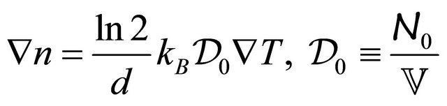
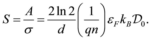
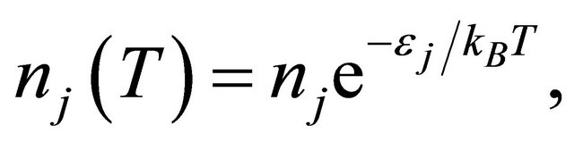
Based on the idea that different temperatures generate different conduction electron densities and the resulting carrier diffusion generates the thermal electromotive force (emf), a new formula for the Seebeck coefficient (thermopower) S is obtained: , where
  is the Boltzmann constant, and
  are charge, carrier density, Fermi energy, density of states at
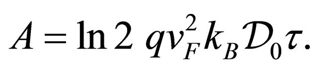
 , respectively. Ohmic and Seebeck currents are fundamentally different in nature, and hence, cause significantly different behaviors. For example, the Seebeck coefficient S in copper (Cu) is positive, while the Hall coefficient is negative. In general, the Einstein relation between the conductivity and the diffusion coefficient does not hold for a multicarrier metal. Multi-walled carbon nanotubes are superconductors. The Seebeck coefficient S is shown to be proportional to the temperature T above the superconducting temperature Tc based on the model of Cooper pairs as carriers. The S follows a temperature behavior,
  , where
 , at the lowest temperatures.
1. Introduction
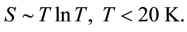
In 2003 Lu et al. and Kang et al. [1,2] observed a logarithmic temperature  -dependence of the seebeck coefficient S in multiwalled carbon nanotubes (MWNTs) at low temperatures. Their data are reproduced in Figure 1 after Ref. [2], Figure 2, where
 ![]() are plotted on a logarithmic temperature scale. Above 20 K the S is proportional to T:
are plotted on a logarithmic temperature scale. Above 20 K the S is proportional to T:
 (1)
(1)
Below 20 K the curves follow the logarithmic behavior:
 (2)
(2)
The data are shown for three samples with different doping levels: A, B and C. If a system of free electrons with a uniform distribution of impurities is considered, then the Seebeck coefficient, also called the thermoelectric power, S is temperature-independent which will be shown in Section 2. Hence the T-behavior in both Equations (1) and (2) are unusual. If the Cooper pairs (pairons) [3] are charge carriers and other conditions are met, then both Equations (1) and (2) are explained microscopically, which is shown in the present work.
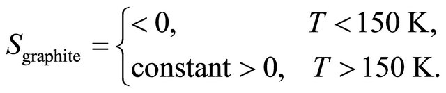
The extended data up to 300 K obtained by Kang et al. [2] are shown in Figure 2, after Ref. [2], Figure 1. In the upper panel the S of MWNT is shown, indicating a clear suppression of S from linearity below 20 K at the lowerright inset. In the lower panel, the Seebeck coefficient S of highly oriented pyrolytic graphite (HOPG), single crystal, is shown. This S is negative (“electron”-like) at low temperatures and become positive (“hole”-like) and constant above 150 K:
 (3)
(3)
The “electron” (“hole”) is a quasi-electron which has an energy higher (lower) than the Fermi energy and which circulates counterclockwise (clockwise) viewed from the tip of the applied magnetic field vector. “Elec-
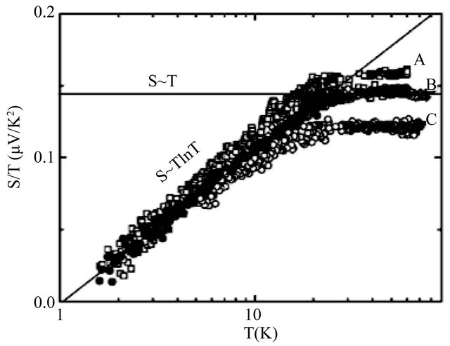
Figure 1. Low temperature seebeck coefficient S of MWNTs plotted as S/T on a logarithmic temperature scale (reproduced from Ref. [2], Figure 2).
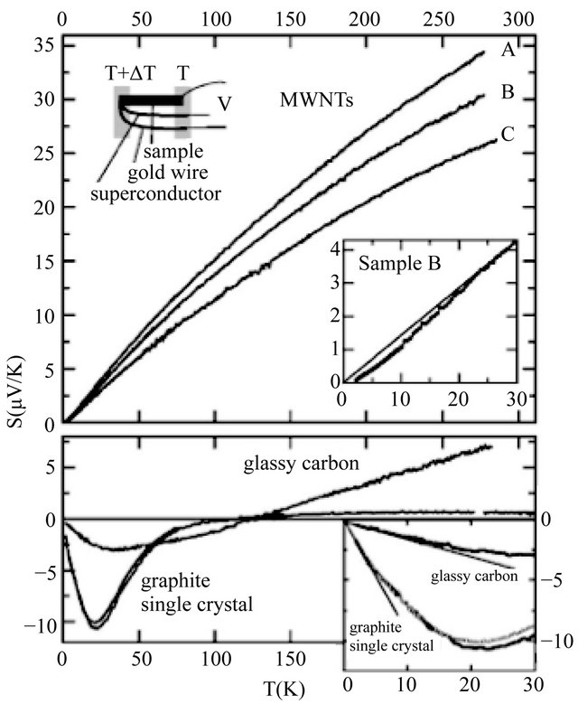
Figure 2. Upper panel: The temperature dependence of thermoelectric power of MWNTs at several doping levels. The suppression of TEP from linearity at low temperatures is clearly shown in the lower-right inset (the line represents a linear T dependsnce). Lower Panel: The thermoelectricic power of HOPG single crystal and glassy carbons. No suppression can be recognized for both as  (reproduced from Ref. [2], Figure 1).
trons” (“holes”) are excited on the positive (negative) side of the Fermi surface with the convention that the positive normal vector at the surface points in the energyincreasing direction. Graphite is composed of ABABtype graphene layers. The different T-behaviors for graphite (3D) and MWNT (2D) should arise from the different carriers. We will show that the majority carriers in graphene and graphite are “electrons” while the majority carriers in MWNT are “holes” based on the Cartesian unit cell model, which is shown in Sections 4 and 5. In this paper, conduction electrons are denoted by quotation marked “electrons” (“holes”) whereas generic electrons are denoted without quotation marks.
2. Theory of the Seebeck Coefficient in a Metal
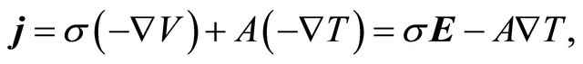
When a metallic bar is subjected to a voltage (V) or temperature (T) difference, an electric current is generated. For small voltage and temperature gradients we may assume a linear relation between the electric current density  and the gradients:
 (4)
(4)
where 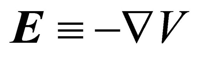 is the electric field and
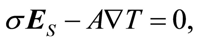
 ![]() the conductivity. If the ends of the conducting bar are maintained at different temperatures, no electric current flows. Thus from Equation (4), we obtain
the conductivity. If the ends of the conducting bar are maintained at different temperatures, no electric current flows. Thus from Equation (4), we obtain
 (5)
(5)
where  is the field generated by the Seebeck electromotive force (emf). The Seebeck coefficient S is defined through
 (6)
(6)
The conductivity ![]() is positive, but the Seebeck coefficient S can be positive or negative. The measured Seebeck coefficient S in Al at high temperatures (400˚C - 670˚C) is negative, while the S in noble metals (Cu, Ag, Au) are positive as shown in Figure 3.
is positive, but the Seebeck coefficient S can be positive or negative. The measured Seebeck coefficient S in Al at high temperatures (400˚C - 670˚C) is negative, while the S in noble metals (Cu, Ag, Au) are positive as shown in Figure 3.
Based on the classical idea that different temperatures generate different electron drift velocities, we obtain
 (7)
(7)
where  is the heat capacity per unit volume and n the
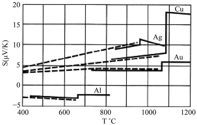
Figure 3. High temperature Seebeck coefficients above 400˚C for Ag, Al, Au, and Cu. The solid and dashed lines represent two experimental data sets. Taken from Ref. [4].
electron density. Setting  equal to
 , we obtain the classical formula for
![]() :
:
 (8)
(8)
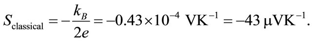
Observed Seebeck coefficients in metals at room temperature are of the order of microvolts per degree (see Figure 3), a factor of 10 smaller than . If we introduce the Fermi-statistically computed heat capacity [5]
 (9)
(9)
where  is the Fermi energy (temperature), in Equation (7), we then obtain
 (10)
(10)
This formula for S is often quoted in materials handbook [4]. Formula (10) remedies the difficulty with respect to the magnitude. But the correct theory must explain the two possible signs of S besides the magnitude.
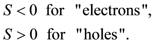
We assume that the carriers are conduction electrons (“electron”, “hole”) with charge  (
(![]() for “electron”,
for “electron”,  for “hole”) and effective mass
 . Assuming a one-component system, the Drude conductivity
 ![]() is given by
is given by
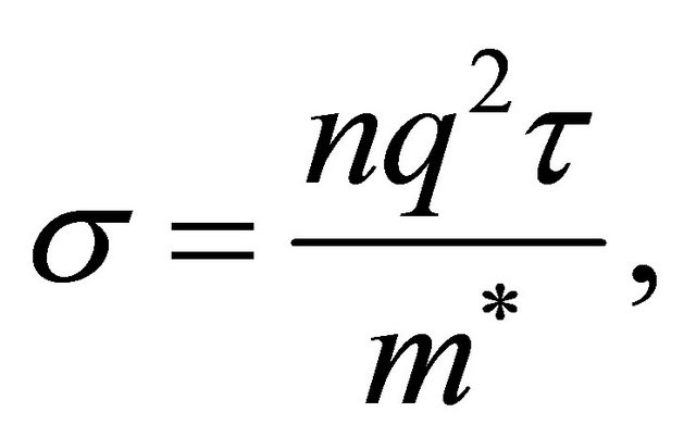 (11)
(11)
where ![]() is the carrier density and
is the carrier density and ![]() the mean free time. We observe from Equation (11) that
the mean free time. We observe from Equation (11) that ![]() is always positive irrespective of whether
is always positive irrespective of whether  or
or . The Fermi distribution function f is
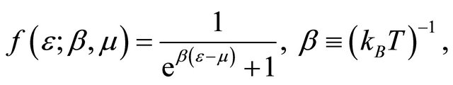 (12)
(12)
where  is the chemical potential whose value at 0 K equals the Fermi energy
 . The voltage difference
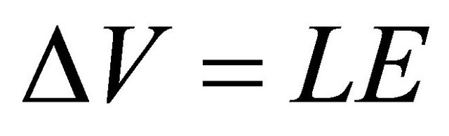 , with
 ![]() being the sample length, generates the chemical potential difference
being the sample length, generates the chemical potential difference , the change in f, and consequently, the electric current. Similarly, the temperature difference
  generates the change in f and the current.
At 0 K the Fermi surface is sharp and there are no conduction electrons (“electrons”, “holes”). At a finite T, “electrons” (“holes”) are thermally excited near the Fermi surface if the curvature of the surface is negative (positive), see Figures 4 and 5.
We assume a high Fermi degeneracy:
 (13)
(13)
Consider first the case of “electrons”. The number of thermally excited “electrons”,  , having energies greater than the Fermi energy
  is defined and cal-
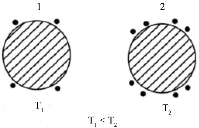
Figure 4. More “electrons” (dots) are excited above the Fermi surface (solid line) at the high temperature end: . The shaded area denotes the electron-filled states. “Electrons” diffuse from 2 to 1.

Figure 5. More “holes” (open circles) are excited below the Fermi surface at the high temperature end: . “Holes” diffuse from 2 to 1.
culated as
 (14)
(14)
where  and
and  is the density of states. The excited “electron” density
 , where
  is the sample volume, is higher at the high-temperature end, and the particle current runs from the highto the lowtemperature end. This means that the electric current runs towards (away from) the high-temperature end in an “electron” (“hole”)-rich material. After using Equations (1) and (14), we obtain
 (15)
(15)
The Seebeck current arises from the thermal diffusion. We assume Fick’s law:
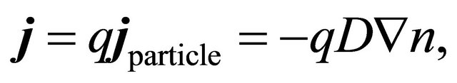 (16)
(16)
where D is the diffusion constant, which is computed from the kinetic-theoretical formula:
 (17)
(17)
where ![]() is the dimension. The density gradient
is the dimension. The density gradient  is generated by the temperature gradient
 , and is given by
 (18)
(18)
where Equation (14) is used. Using the last three equations and Equation (11), we obtain
 (19)
(19)
Using Equations (11), (13) and (19), we obtain
 (20)
(20)
The mean free time ![]() cancels out from numerator and denominator.
cancels out from numerator and denominator.
The derivation of our formula [Equation (20)] for the Seebeck coefficient S was based on the idea that the Seebeck emf arises from the thermal diffusion. We used the high Fermi degeneracy condition (13):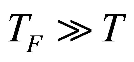 . The relative errors due to this approximation and due to the neglect of the T-dependence of
  are both of the order
 . Formula (20) can be negative or positive, while the materials handbook formula (10) has the negative sign. The average speed
 ![]() for highly degenerate electrons is equal to the Fermi velocity
for highly degenerate electrons is equal to the Fermi velocity  (independent of
![]() ). In Ashcroft and Mermin’s book [5], the origin of a positive
). In Ashcroft and Mermin’s book [5], the origin of a positive ![]() in terms of a mass tensor
in terms of a mass tensor
 is discussed. This tensor
  is real and symmetric, and hence, it can be characterized by the principal masses
 . Formula for
 ![]() obtained by Ashcroft and Mermin (Equation (13.62) in Ref. [5]), can be positive or negative but is hard to apply in practice. In contrast our formula (20) can be applied straightforwardly. Besides our formula for a one-carrier system is
obtained by Ashcroft and Mermin (Equation (13.62) in Ref. [5]), can be positive or negative but is hard to apply in practice. In contrast our formula (20) can be applied straightforwardly. Besides our formula for a one-carrier system is ![]() -independent, while the AM formula is linear in
-independent, while the AM formula is linear in![]() .
.
Formula (20) is remarkably similar to the standard formula for the Hall coefficient of a one-component system:
 (21)
(21)
Both Seebeck and Hall coefficients are inversely proportional to charge , and hence, they give important information about the carrier charge sign. In fact the measurement of the S of a semiconductor can be used to see if the conductor is n-type or p-type (with no magnetic measurements). If only one kind of carrier exists in a conductor, then the Seebeck and Hall coefficients must have the same sign as observed in alkali metals.
Let us consider the electric current caused by a voltage difference. The current is generated by the electric force that acts on all electrons. The electron’s response depends on its mass . The density
  dependence of
 ![]() can be understood by examining the current-carrying steady state in Figure 6(b). The electric field
can be understood by examining the current-carrying steady state in Figure 6(b). The electric field  displaces the electron distribution by a small amount
  from the equilibrium distribution in Figure 6(a).
Since all the conduction electron are displaced, the conductivity ![]() depends on the particle density
depends on the particle density![]() . The Seebeck current is caused by the density difference in the thermally excited electrons near the Fermi surface, and hence, the thermal diffusion coefficient
. The Seebeck current is caused by the density difference in the thermally excited electrons near the Fermi surface, and hence, the thermal diffusion coefficient  depends on the density of states at the Fermi energy,
  [see Equation (19)]. We further note that the diffusion coefficient
  does not depend on
  directly [see Equation (17)]. Thus, the Ohmic and Seebeck currents are fundamentally different in nature.
For a single-carrier metal such as sodiuml (Na) which forms a body-centered-cubic (bcc) lattice, where only “electrons” exist, both  and S are negative. The Einstein relation between the conductivity
 ![]() and the diffusion coefficient D holds:
and the diffusion coefficient D holds:
 (22)
(22)
Using Equations (11) and (17), we obtain
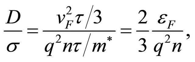 (23)
(23)
which is a material constant. The Einstein relation is valid for a single-carrier system.
3. Simple Applications
We consider two-carrier metals (noble metals). Noble metals including copper (Cu), silver (Ag) and gold (Au) form face-centered cubic (fcc) lattices. Each metal contains “electrons” and “holes”. The Seebeck coefficient S for these metals are shown in Figure 3. The S is positive for all:
 (24)
(24)
indicating that the major carriers are “holes”. The Hall coefficient  is known to be negative:
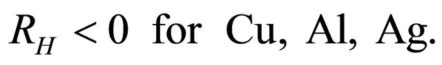 (25)
(25)
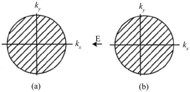
Figure 6. Due to the electric field E pointed in the negative x-direction, the steady-state electron distribution in (b) is generated by a translation of the equilibrium distribution in (a) by the amount .
.
Clearly the Einstein relation (22) does not hold since the charge sign is different for ![]() and
and . This complication was explained by Fujita, Ho and Okamura [6] based on the Fermi surfaces having “necks” (see Figure 7). The curvatures along the axes of each neck are positive, and hence, the Fermi surface is “hole”-generating. Experiments [7-9] indicate that the minimum neck area
  (neck) in the
  -space is
 ![]() of the maximum belly area
of the maximum belly area  (belly), meaning that the Fermi surface just touches the Brillouin boundary (Figure 7 exaggerates the neck area). The density of “hole”-like states,
  associated with the
  necks, having the heavy-fermion character due to the rapidly varying Fermi surface with energy, is much greater than that of “electron”-like states,
  , associated with the
  belly. The thermally excited “hole” density is higher than the “electron” density, yielding a positive
![]() . The principal mass
. The principal mass  along the axis of a small neck
 is positive (“hole”-like) and extremely large. The “hole” contribution to the conduction is small
 . Then the “electrons” associated with the nonneck Fermi surface dominate and yield a negative Hall coefficient
 .
.
The Einstein relation (22) does not hold in general for multi-carrier systems. The currents are additive. The ratio  for a two-carrier system containing “electrons” (1) and “holes” (2) is given by
 (26)
(26)
which is a complicated function of
 , and
, and . In particular the mass ratio
  may vary significantly for a heavy fermion condition, which occurs whenever the Fermi surface just touches the Brillouin boundary. An experimental check on the violation of the Einstein relation can be carried out by simply examining the T dependence of the ratio
 . This ratio
  depends on T since the generally T-dependent mean free times
  arising
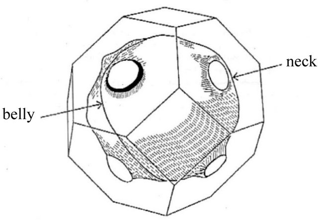
Figure 7. The Fermi surface of silver (fcc) has “necks”, with the axes in the  direction, located near the Brillouin boundary, reproduced after Refs. [7-9].
from the electron-phonon scattering do not cancel out from numerator and denominator. Conversely, if the Einstein relation holds for a metal, the spherical Fermi surface approximation with a single effective mass  is valid.
4. Graphene and Carbon Nanotubes
Graphite and diamond are both made of carbons. They have different lattice structures and different properties. Diamond is brilliant and it is an insulator while graphite is black and is a good conductor. In 1991 Iijima [10] discovered carbon nanotubes in the soot created in an electric discharge between two carbon electrodes. These nanotubes ranging 4 to 30 nanometers (nm) in diameter are found to have helical multi-walled structure. The tube length is about one micron (μm). Single-wall nanotubes (SWNT) were fabricated first by Iijima and Ichihashi [11] and by Bethune et al. [12] in 1993. The tube size is about one nanometer in diameter and a few microns in length. The scroll-type tube is called the multi-walled carbon nanotube (MWNT). The tube size is about ten nanometers in diameter and a few microns (μ) in length. Unrolled carbon sheet are called graphene, which has a honeycomb lattice structure as shown in Figure 8.
We consider a graphene which forms a two-dimensional (2D) honeycomb lattice. The normal carriers in the electrical charge transport are “electrons” and “holes”. Following Ashcroft and Mermin [5], we assume the semiclassical (wave packet) model of a conduction electron. It is necessary to introduce a  -vector:
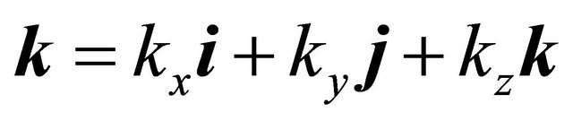 (27)
(27)
since the  -vector is involved in the semiclassical equation of motion:
 (28)
(28)
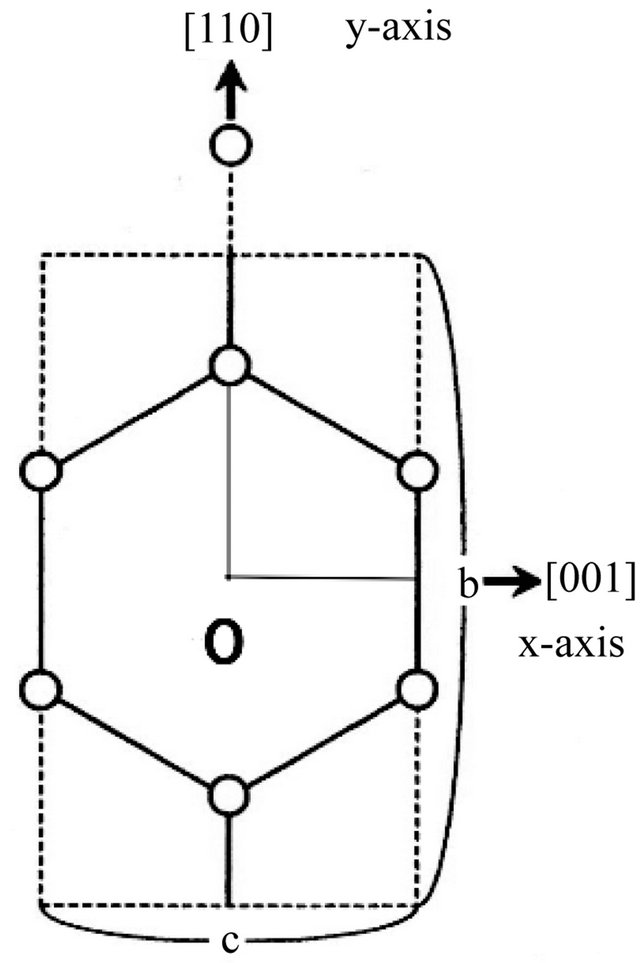
Figure 8. The Cartesian unit cell (dotted line) contains four (4) C’s (open circles).
where  and
and  are the electric and magnetic fields, respectively. The vector
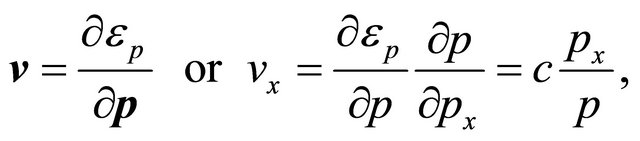
 (29)
(29)
is the particle velocity, where ![]() is the particle energy. For some crystals such as simple cubic, face-centered cubic, body-centered-cubic, tetragonal, and orthorhombic crystals, the choice of the orthogonal
is the particle energy. For some crystals such as simple cubic, face-centered cubic, body-centered-cubic, tetragonal, and orthorhombic crystals, the choice of the orthogonal  -axes and the unit cells are obvious. The 2D crystals such as graphene can also be treated similarly, only the z-component being dropped. We will show that graphene has “electrons” and “holes” based on the rectangular unit cell model.
We assume that the “electron” (“hole”) wave packet has the charge  and a size of a unit carbon hexagon, generated above (below) the Fermi energy
 . We will show that (a) the “electron” and “hole” have different charge distributions and different effective masses, (b) that the “electrons” and “holes” are thermaly activated with different energy gaps
 , and (c) that the “electrons” and “holes” move in different easy channels in which they travel.
The positively-charged “hole” tends to stay away from positive ions C+, and hence its charge is concentrated at the center of the hexagon. The negatively charged electron tends to stay close to the C+ hexagon and its charge is concentrated near the C+ hexagon. In our model, the “electron” and “hole” both have sizes and charge distributions, and they are not point particles. Hence, their masses  and
and  must be different from the gravitational mass m = 9.11 × 10⁻²⁸ g. Because of the different internal charge distributions, the “electrons” and “holes” have the different effective masses
  and
and . The “electron” may move easily with a smaller effective mass in the direction
  than perpen-dicular to it as we see presently. Here, we use the conventional Miller indices for the hexagonal lattice with omission of the
 ![]() -axis index. For the description of the electron motion in terms of the mass tensor. It is necessary to introduce Cartesian coordinates, which do not match with the crystal’s natural (triangular) axes. We may choose the unit cell as shown in Figure 8. Then the Brillouin zone boundary in the
-axis index. For the description of the electron motion in terms of the mass tensor. It is necessary to introduce Cartesian coordinates, which do not match with the crystal’s natural (triangular) axes. We may choose the unit cell as shown in Figure 8. Then the Brillouin zone boundary in the  space is a rectangle with side lengths
 . The “electron” (wave packet) may move up or down in
  to the neighboring hexagon sites passing over one C+. The positively charged C+ acts as a welcoming (favorable) potential valley center for the negatively charged “electron” while the same C+ acts as a hindering potential hill for the positively charged “hole”. The “hole” can however move easily horizontally without meeting the hindering potential hills. Then, the easy channel directions for the “electrons” and “holes” are
  and
and , respectively.
Let us consider the system (graphene) at 0 K. If we put an electron in the crystal, then the electron should occupy the center O of the Brillouin zone, where the lowest energy lies. Additional electrons occupy points neighboring O in consideration of Pauli’s exclusion principle. The electron distribution is lattice-periodic over the entire crystal in accordance with the Bloch theorem. The uppermost partially filled bands are important for the transport properties discussion. We consider such a band. The 2D Fermi surface which defines the boundary between the filled and unfilled  -space (area) is not a circle since the
  symmetry is broken. The “electron” effective mass is smaller in the direction
  than perpendicular to it. That is, the system has two effective masses and it is intrinsically anisotropic. If the electron number is raised by the gate voltage, then the Fermi surface more quickly grows in the easy-axis
  direction, say
  than in the
 ![]() -direction, i.e.,
-direction, i.e., . The Fermi surface must approach the Brillouin boundary at right angles because of the inversion symmetry possessed by the honeycomb lattice. Then at a certain voltage, a “neck” Fermi surface must be developed.
The same easy channels in which the “electron” runs with a small mass, may be assumed for other hexagonal directions,  and
and . The currents run in three channels
 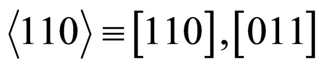 and
and . The effective electric field along a channel
  is reduced by the directional cosine
 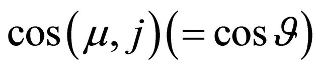 between the field direction
  and the channel direction
 . The current is reduced by the same factor in the Ohmic conduction. The total current is the sum of the channel currents. Then its component along the field direction is proportional to
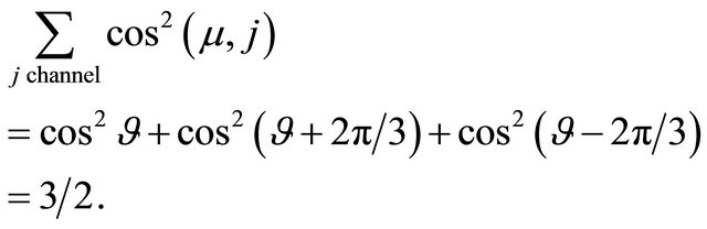 (30)
(30)
There is no angle  dependence. The number
  represents the fact that the current density is higher by this factor for a honeycomb lattice than for the square lattice. The “holes” run in three easy channels
 and
and . (We note that the channel directions are separated by
 .) The total currents run isotropically for the “holes”, too.
We have seen that the “electron” and “hole” have different internal charge distributions and therefore have different effective masses. Which carriers are easier to be activated or excited? The “electron” is near the positive ions and the “hole” is farther away from the ions. Hence, the gain in the Coulomb interaction is greater for the “electron”. That is, the “electrons” are more easily activated (or excited). The “electrons” move in the welcoming potential-well channels while the “holes” do not.
This fact also leads to the smaller activation energy for the “electrons”. We may represent the activation energy  difference by
 (31)
(31)
From this we conclude that “electrons” are the majority carriers in graphene. The same holds in graphite, which is shown in Appendix.
The thermally activated electron densities are then given by [13]
 (32)
(32)
where  and 2 represent the “electron” and “hole”, respectively. The prefactor
  is the density at the high temperature limit.
5. Conduction in Multi-Walled Carbon Nanotubes
MWNTs are open-ended. Hence, each pitch is likely to contain an irrational number of carbon hexagons. Then, the electrical conduction of MWNT is similar to that of metallic SWNT [14].
Phonons are excited based on the same Cartesian unit cell as the conduction electrons in the carbon wall. The phonon exchange interaction bounds Cooper pairs, also called pairons [3].
The conductivity ![]() based on the pairon carrier model is calcullated as follows. The pairons move in 2D with the linear dispersion relation [3]:
based on the pairon carrier model is calcullated as follows. The pairons move in 2D with the linear dispersion relation [3]:
 (33)
(33)
 (34)
(34)
where  is the Fermi velocity of the “electron”
  [“hole”
 ].
].
Consider first “electron”-pairs. The velocity ![]() is given by (omitting superscript)
is given by (omitting superscript)
 (35)
(35)
where we used Equation (33) for the pairon energy  and the 2D momentum,
 (36)
(36)
The equation of motion along the electric field  in the
 ![]() -direction is
-direction is
 (37)
(37)
where  is the charge
  of a pairon. The solution of Equation (37) is given by
 (38)
(38)
where  is the initial momentum component. The current density jp is calculated from
 .
.
The average velocity  is calculated by using Equation (35) and Equation (38) with the assumption that the pair is accelerated only for the mean free time
 ![]() and the initial-momentum-dependent terms are averaged out to zero. We then obtain
and the initial-momentum-dependent terms are averaged out to zero. We then obtain
 (39)
(39)
For stationary currents, the partial pairon density  is given by the Bose distribution function
 :
:
 (40)
(40)
where  is the fugacity. Integrating the current
  over all 2D
 ![]() -space, and using Ohm’s law
-space, and using Ohm’s law , we obtain for the conductivity
![]() :
:
![]() (41)
(41)
In the low temperatures we may assume the Boltzmann distribution function for :
:
 (42)
(42)
We assume that the relaxation time arises from the phonon scattering so that
 (43)
(43)
After performing the ![]() -integration we obtain from Equation (41)
-integration we obtain from Equation (41)
 (44)
(44)
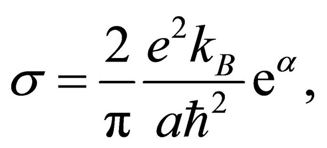
which is temperature-independent. If there are “electrons” and “hole” pairons, they contribute additively to the conductivity. These pairons should undergo a BoseEinstein condensation at lowest temperatures.
6. Seebeck Coefficient in Multi-Walled Carbon Nanotubes
We are now ready to discuss the Seebeck coefficient S of MWNT. First, we will show that the S is proportional to the temperature T above the superconducting temperature .
.
We start with the standard formula for the charge current density:
 (45)
(45)
where ![]() is the average velocity, which is a function of temperature T and the particle density n:
is the average velocity, which is a function of temperature T and the particle density n:
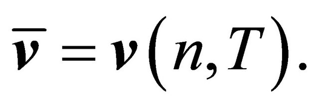 (46)
(46)
We assume a steady state of the system in which the temperature T varies only in the ![]() -direction while the density is kept constant. The temperature gradient
-direction while the density is kept constant. The temperature gradient  generates a current:
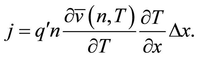 (47)
(47)
The thermal diffusion occurs locally. We may choose  to be a mean free path:
 (48)
(48)
The current density,  , at the 2D pairon momentum
![]() , which is generated by the temperature gradient
, which is generated by the temperature gradient , is thus given by
 (49)
(49)
Integrating Equation (49) over all 2D ![]() -space and comparing with Equation (4), we obtain
-space and comparing with Equation (4), we obtain
 (50)
(50)
We compare this integral with the integral in Equation (41). It has an extra factor in ![]() and generates therefore an extra factor
and generates therefore an extra factor ![]() when the Boltzmann distribution function is adopted for
when the Boltzmann distribution function is adopted for . Thus, we obtain, using Equations (41) and (50),
 (51)
(51)
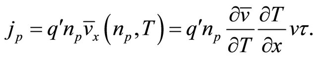
We next consider the system below the superconducting temperature . The supercurrents arising from the condensed pairons generate no thermal diffusion. But non-condensed pairons can be scattered by impurities and phonons, and contribute to a thermal diffusion. Because of the zero-temperature energy gap
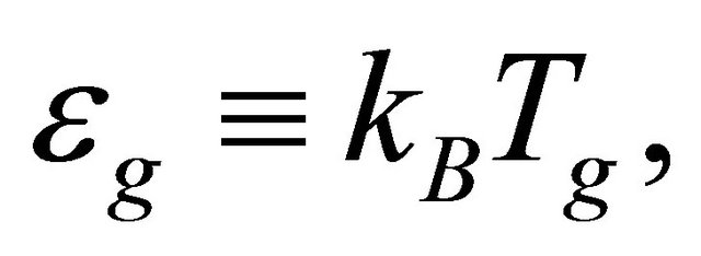 (52)
(52)
generated by the supercondensate, the population of the non-condensed pairons is reduced by the BoltzmannArrhenius factor
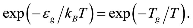 (53)
(53)
This reduction applies only for the conductivity (but not for the diffusion). Hence we obtain the Seebeck coefficient:
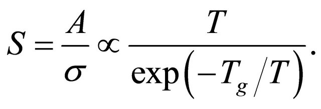 (54)
(54)
In the experiment [1,2] MWNT bundles containing hundreds of individual nanotubes are used. Both circumference and pitch have distributions. Hence, the energy gap 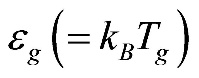 has a distribution.
Kang et al. [2] measured the conductance , which is proportional to the conductivity
![]() , of the MWNT samples. Their data are reproduced in Figure 9, after Ref. [2], Figure 3, where the conductance
, of the MWNT samples. Their data are reproduced in Figure 9, after Ref. [2], Figure 3, where the conductance  as a function of temperature is plotted on a logarithmic scale.
The  arising from the conduction electron in each MWNT carries an Arrhenius-type exponential
 (55)
(55)
where  is the activation energy. This energy
  has a distribution since the MWNT have varied circumferences and pitches. The temperature behavior of
  for the bundle of MWNT is seen to be represented by
 (56)
(56)
in the range: 5 - 20 K. The electron-activation energy 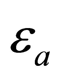 and the zero-temperature pairon energy gap
  are different from each other. But they have the same orders of magnitude and both are temperature-independent. We assume that the distributions are similar. We may then replace
  in Equation (54) by
 obtaining the Seebeck coefficient for a bundle of MWNTs
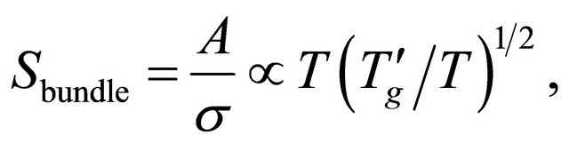 (57)
(57)
or
 (58)
(58)
which is observed in Figure 1.
The data in Figure 1 clearly indicates a phase change at the temperature
 (59)
(59)
We now discuss the connection between this  and the superconducting temperature
 . We deal with a thermal
Figure 9. The conductance G of the multi-walled carbon nanotube samples as a function of temperature (after Ref. [2], Figure 3).
diffusion of the MWNT bundle. The diffusion occurs most effectively for the most dissipative samples which correspond to those with the lowest superconducting temperatures. Hence, the 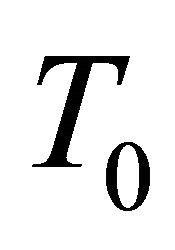 observed can be interpreted as the superconducting temperature of the most dissipative samples.
In contrast the conduction is dominated by the least dissipative samples having the highest . Figure 3 shows a clear deviation of
 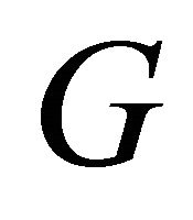 around 120 K from the experimental law:
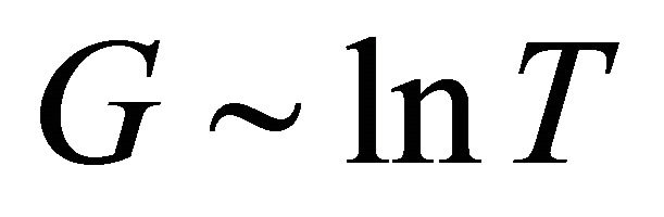 . We may interpret this as an indication of the limit of the superconducting states. We then obtain
 (60)
(60)
for the good samples.
By considering moving pairons we obtained the Tlinear behavior of the Seebeck coefficient S above the superconducting temperature Tc and the  -behavior of
 ![]() at the lowest temperatures. The energy gap
at the lowest temperatures. The energy gap  vanishes at
 . Hence, the temperature behaviors should be smooth and monotonic as observed in Figure 1. This supports our interpretation of the data based on the superconducting phase transition. The doping changes the pairon density and the superconducting temperature. Hence the data for A, B and C in Figure 1 are reasonable.
7. Conduction Electrons in Graphite
Graphite is composed of graphene layers stacked in the manner ABAB along the
 ![]() -axis. We may choose a Cartesian unit cell as shown in Figure 10.
-axis. We may choose a Cartesian unit cell as shown in Figure 10.
The rectangle (white solid line) in the A plane (blue) contains six (6) C’s wholely within and four (4) C’s at sides. The side C’s are shared by neighbors. Hence the total number of C’s is . The rectangle in the B plane (orange) contains five (5) C’s within and four (4) C’s at sides and four (4) C’s at corners. The total number of C’s is
 . The unit cell contains 16 C’s. The two rectangles are stacked vertically with the interlayer separation,
  Å much greater than the nearest neighbor distance between two C’s,
  Å. The unit cell has three side-lengths:
 (61)
(61)
The center of the unit cell is empty. Clearly, the system is periodic along the orthogonal directions with the three periods  given in Equation (61). We assume that both “electron” and “hole” have the same unit cell size. In summary the system is orthorhombic with the sides
The negatively charged “electron” (with the charge −e) in graphite are welcomed by the positively charged C when moving in the direction  just as in graphene.
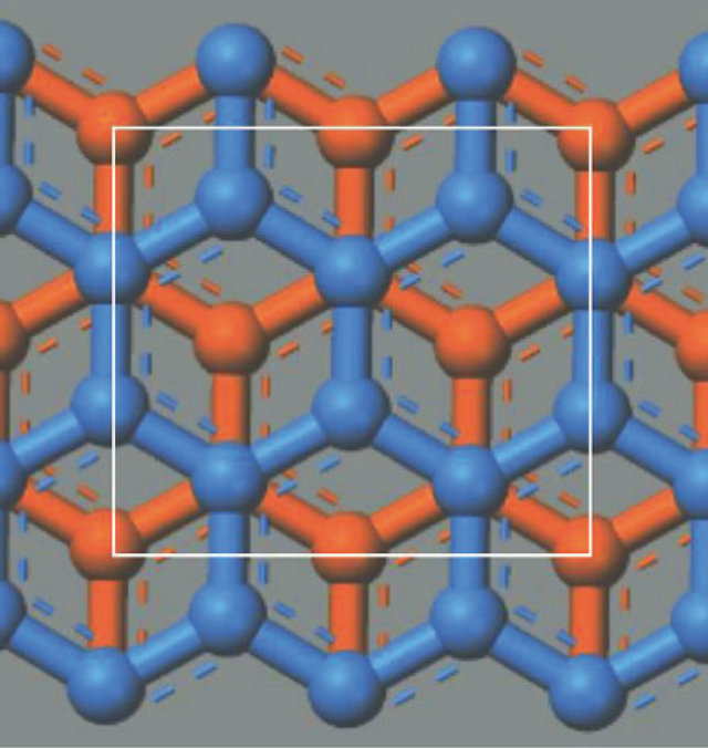
Figure 10. The Cartesian unit cell (white solid lines) viewed from the top. The carbons (circles) in the A (B) planes are shown in blue (orange).
That is, the easy directions for the “electrons” are .
.
Similarly, the easy directions for the “holes” are .
.
There are no hindering hills for “holes” moving in . Hence just as graphene, the “electron” in graphite has the lower activation energy
 ![]() than the “hole”:
than the “hole”:
 (62)
(62)
Then, the “electrons” are the majority carriers in graphite.
REFERENCES
- L. Lu, N. Kang, W. J. Kong, D. L. Zhang, Z. W. Pan and S. S. Xie, Physica E, Vol. 18, 2003, pp. 214-215. doi:10.1016/S1386-9477(02)00971-2
- N. Kang, L. Lu, W. J. Kong, J. S. Hu, W. Yi, Y. P. Wang, D. L. Zhang, Z. W. Pan and S. S. Xie, Physical Review B, Vol. 67, 2003, pp. 033404-033408. doi:10.1103/PhysRevB.67.033404
- S. Fujita, K. Ito and S. Godoy, “Quantum Theory of Conducting Matter. Superconductivity,” Springer, New York, 2009, pp. 77-79. doi:10.1007/978-0-387-88211-6
- P. L. Rossiter and J. Bass, “Encyclopedia of Applied Physics,” Wiley-VCH Publ., Berlin, 1994, pp. 163-197.
- N. W. Ashcroft and N. D. Mermin, “Solid State Physics,” Saunders, Philadelphia, 1976, pp. 46-47, 217-218, 256-258, 290-293.
- S. Fujita, H.-C. Ho and Y. Okamura, International Journal of Modern Physics B, Vol. 14, 2000, pp. 2231-2240. doi:10.1142/S0217979200002107
- D. J. Roaf, Philosophical Transactions of the Royal Society A, Vol. 255, 1962, pp. 135-152. doi:10.1098/rsta.1962.0012
- D. Schönberg, Philosophical Transactions of the Royal Society A, Vol. 255, 1962, pp. 85-133. doi:10.1098/rsta.1962.0011
- D. Schönberg and A. V. Gold, “Physics of Metals 1,” In: J. M. Ziman, Ed., Electrons, Cambridge University Press, Cambridge, 1969, p. 112. doi:10.1038/363605a0
- S. Iijima, Nature, Vol. 354, 1991, pp. 56-58. doi:10.1038/354056a0
- S. Iijima and T. Ichihashi, Nature, Vol. 363, 1993, pp. 603-605. doi:10.1038/363603a0
- D. S. Bethune, C. H. Kiang, M. S. de Vries, G. Gorman, R. Savoy, J. Vazquez and R. Beyers, Nature, Vol. 363, 1993, pp. 605-607.
- S. Fujita and A. Suzuki, Journal of Applied Physics, Vol. 107, 2010, pp. 013711-0137115. doi:10.1063/1.3280035
- S. Fujita, Y. Takato and A. Suzuki, Modern Physics Letters B, Vol. 25, 2011, pp. 223-242. doi:10.1142/S0217984911025675
NOTES
*Corresponding author.